Quantum Dots What is a quantum dot In

![QD Energy Spectra Channelled spectra, [110] in and normal out, very similar for uncapped QD Energy Spectra Channelled spectra, [110] in and normal out, very similar for uncapped](https://slidetodoc.com/presentation_image_h/e608ec740f949154eddf4b999cc5ac42/image-83.jpg)
- Slides: 87

Quantum Dots

What is a quantum dot? • In two words, a semiconductor nanocrystal. • Easily tunable by changing the size and composition of the nanocrystal

Gallium Arsenide Quantum Dots • Gallium arsenide is a III-V semiconductor – Higher saturated electron velocity and higher electron mobility than silicon – Gallium arsenide can emit and absorb light, unlike silicon • No silicon laser is possible (or has been made yet)

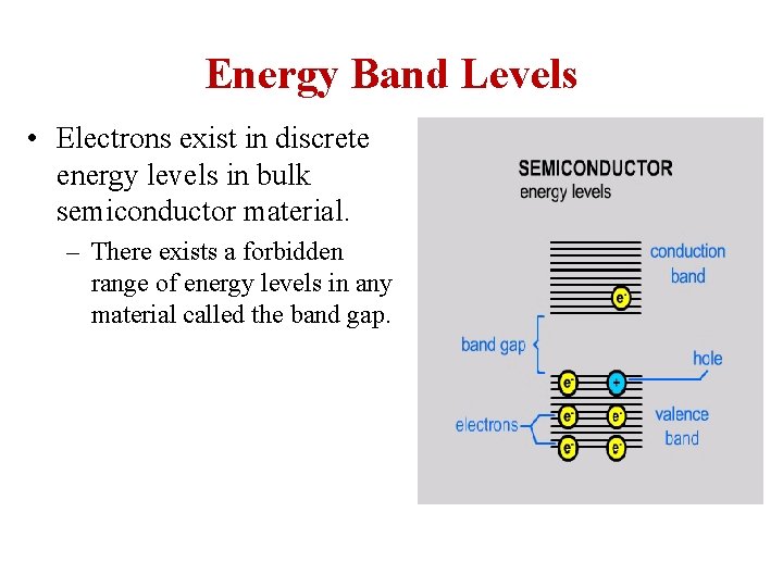
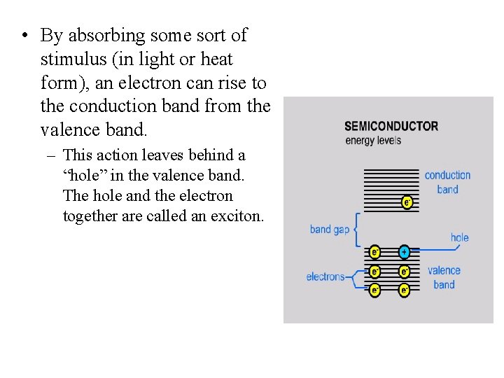
Energy Band Levels • Electrons exist in discrete energy levels in bulk semiconductor material. – There exists a forbidden range of energy levels in any material called the band gap.

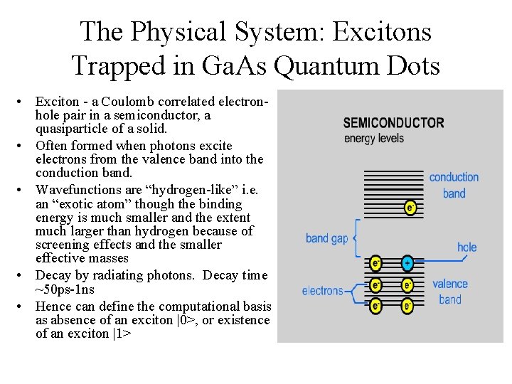
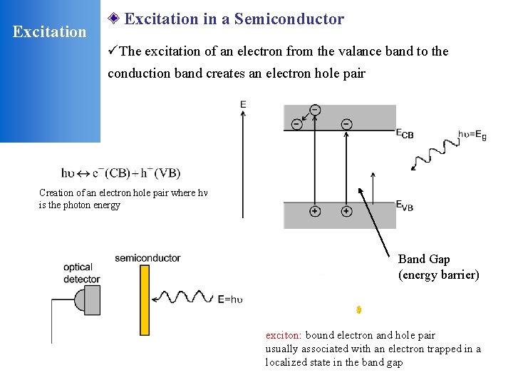
• By absorbing some sort of stimulus (in light or heat form), an electron can rise to the conduction band from the valence band. – This action leaves behind a “hole” in the valence band. The hole and the electron together are called an exciton.

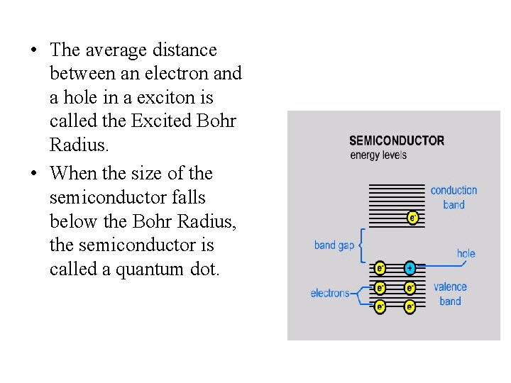
• The average distance between an electron and a hole in a exciton is called the Excited Bohr Radius. • When the size of the semiconductor falls below the Bohr Radius, the semiconductor is called a quantum dot.

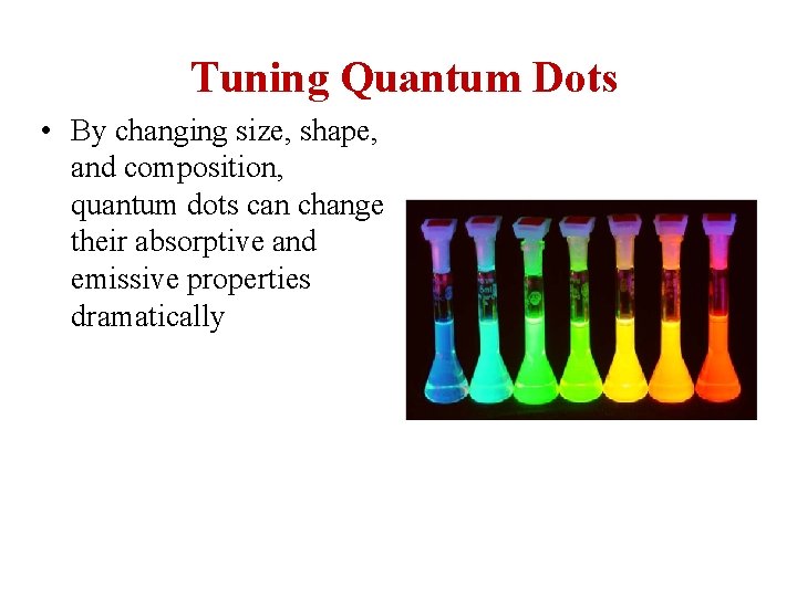
Tuning Quantum Dots • By changing size, shape, and composition, quantum dots can change their absorptive and emissive properties dramatically

Manufacturing methods • Electron beam lithography • Molecular beam epitaxy

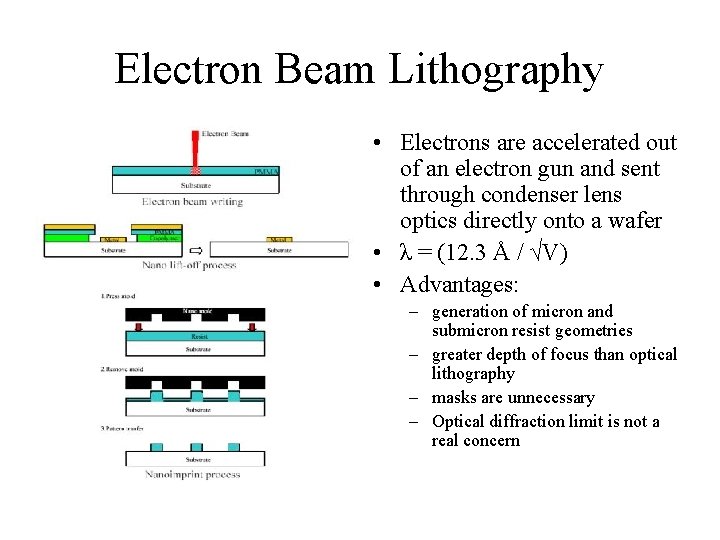
Electron Beam Lithography • Electrons are accelerated out of an electron gun and sent through condenser lens optics directly onto a wafer • λ = (12. 3 Å / √V) • Advantages: – generation of micron and submicron resist geometries – greater depth of focus than optical lithography – masks are unnecessary – Optical diffraction limit is not a real concern

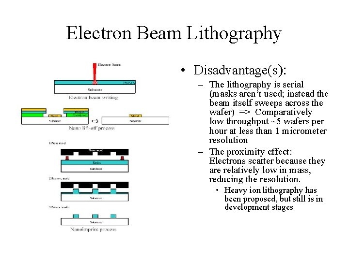
Electron Beam Lithography • Disadvantage(s): – The lithography is serial (masks aren’t used; instead the beam itself sweeps across the wafer) => Comparatively low throughput ~5 wafers per hour at less than 1 micrometer resolution – The proximity effect: Electrons scatter because they are relatively low in mass, reducing the resolution. • Heavy ion lithography has been proposed, but still is in development stages

Molecular Beam Epitaxy • Molecular beam epitaxy (MBE) is the deposition of one or more pure materials onto a single crystal wafer one layer of atoms at a time in order to form a perfect crystal – This is done by evaporating each of the elements to combine, then condensing them on top of the wafer. – The word “beam” means that the evaporated atoms only meet each other on the wafer

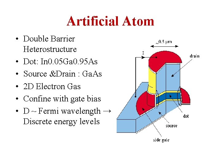
Artificial Atom • Double Barrier Heterostructure • Dot: In 0. 05 Ga 0. 95 As • Source &Drain : Ga. As • 2 D Electron Gas • Confine with gate bias • D ~ Fermi wavelength → Discrete energy levels

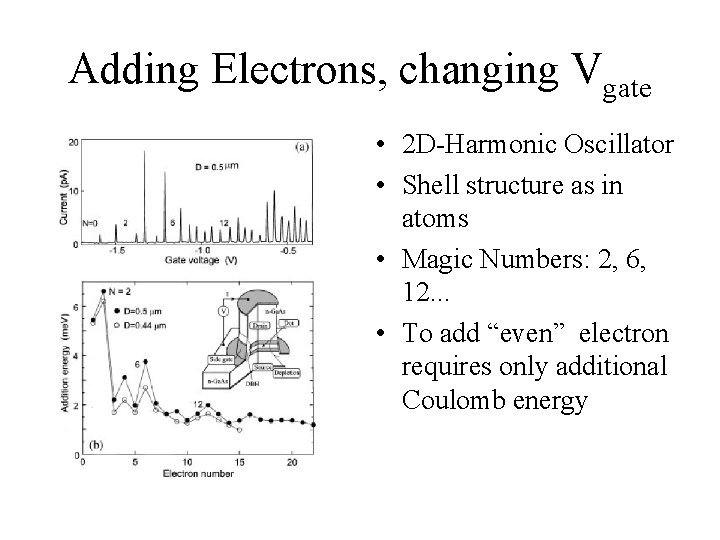
Adding Electrons, changing Vgate • 2 D-Harmonic Oscillator • Shell structure as in atoms • Magic Numbers: 2, 6, 12. . . • To add “even” electron requires only additional Coulomb energy

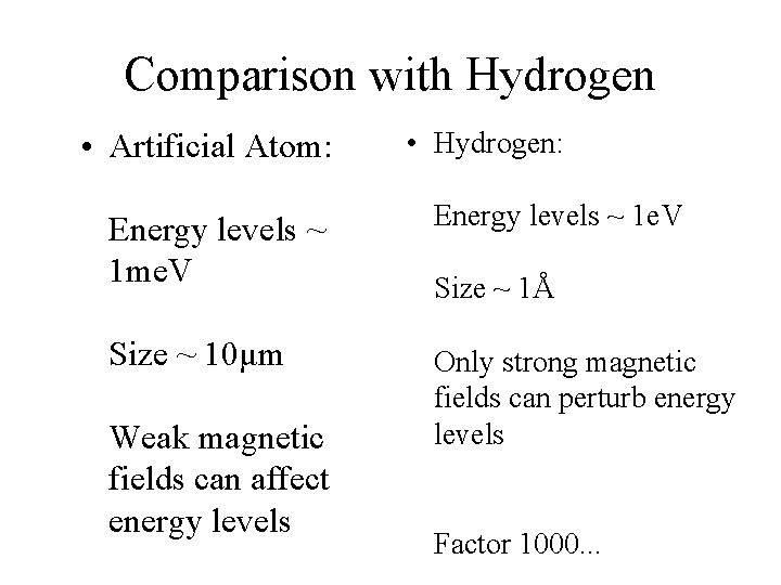
Comparison with Hydrogen • Artificial Atom: • Hydrogen: Energy levels ~ 1 me. V Energy levels ~ 1 e. V Size ~ 10μm Only strong magnetic fields can perturb energy levels Weak magnetic fields can affect energy levels Size ~ 1Å Factor 1000. . .

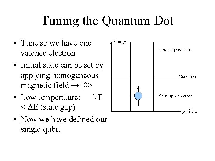
Tuning the Quantum Dot • Tune so we have one valence electron • Initial state can be set by applying homogeneous magnetic field → |0> • Low temperature: k. T < ΔE (state gap) • Now we have defined our single qubit Energy Unoccupied state Gate bias Spin up - electron position

The Physical System: Excitons Trapped in Ga. As Quantum Dots • Exciton - a Coulomb correlated electronhole pair in a semiconductor, a quasiparticle of a solid. • Often formed when photons excite electrons from the valence band into the conduction band. • Wavefunctions are “hydrogen-like” i. e. an “exotic atom” though the binding energy is much smaller and the extent much larger than hydrogen because of screening effects and the smaller effective masses • Decay by radiating photons. Decay time ~50 ps-1 ns • Hence can define the computational basis as absence of an exciton |0>, or existence of an exciton |1>

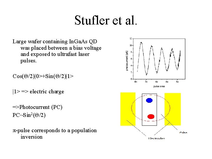
Stufler et al. Large wafer containing In. Ga. As QD was placed between a bias voltage and exposed to ultrafast laser pulses. Cos(Θ/2)|0>+Sin(Θ/2)|1> => electric charge =>Photocurrent (PC) PC~Sin 2(Θ/2) π-pulse corresponds to a population inversion

Saint-Petersburg State University Quantum Dots. Optical and Photoelectrical properties of QD of III-V Compounds. Alexander Senichev Physics Faculty Department of Solid State Physics senichev_spb@mail. ru 8 -921 -5769793

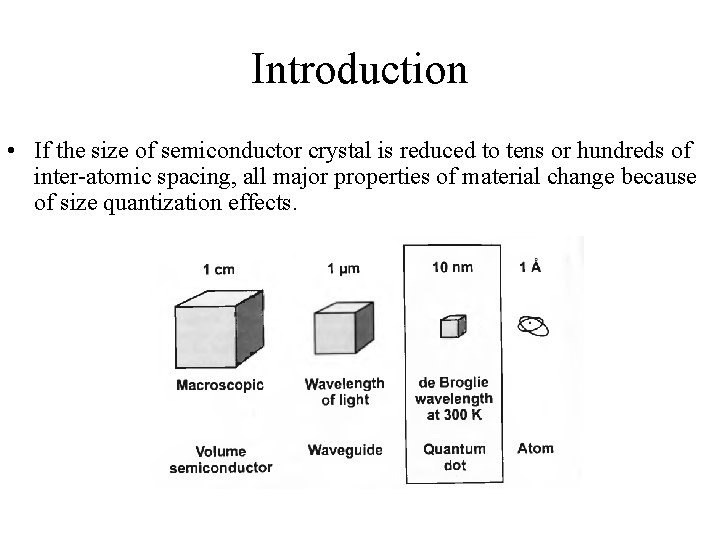
Introduction • If the size of semiconductor crystal is reduced to tens or hundreds of inter-atomic spacing, all major properties of material change because of size quantization effects.

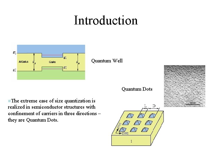
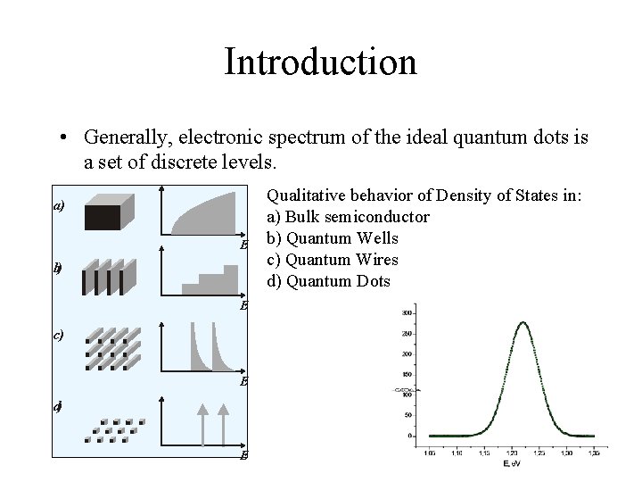
Introduction Quantum Well Quantum Dots n. The extreme case of size quantization is realized in semiconductor structures with confinement of carriers in three directions – they are Quantum Dots.

Introduction • Generally, electronic spectrum of the ideal quantum dots is a set of discrete levels. а) E b) E с) E d) E Qualitative behavior of Density of States in: a) Bulk semiconductor b) Quantum Wells c) Quantum Wires d) Quantum Dots

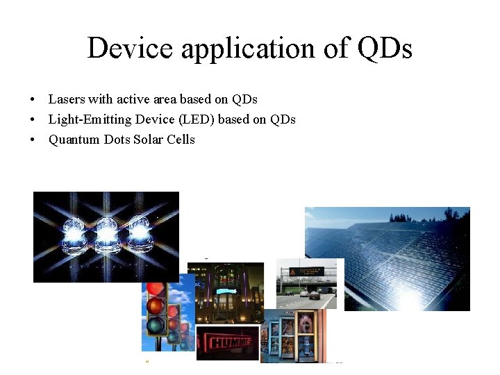
Device application of QDs • Lasers with active area based on QDs • Light-Emitting Device (LED) based on QDs • Quantum Dots Solar Cells

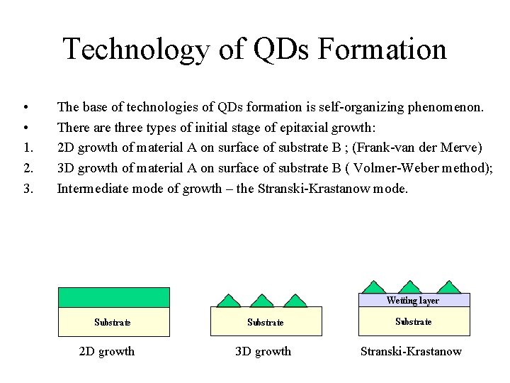
Technology of QDs Formation • • 1. 2. 3. The base of technologies of QDs formation is self-organizing phenomenon. There are three types of initial stage of epitaxial growth: 2 D growth of material A on surface of substrate B ; (Frank-van der Merve) 3 D growth of material A on surface of substrate B ( Volmer-Weber method); Intermediate mode of growth – the Stranski-Krastanow mode. 2 D growth 3 D growth Stranski-Krastanow

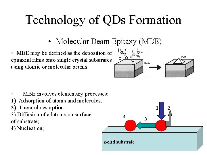
Technology of QDs Formation • Molecular Beam Epitaxy (MBE) § MBE may be defined as the deposition of epitaxial films onto single crystal substrates using atomic or molecular beams. § MBE involves elementary processes: 1) Adsorption of atoms and molecules; 2) Thermal desorption; 3) Diffusion of adatoms on surface of substrate; 4) Nucleation; 1 4 Solid substrate 3 2

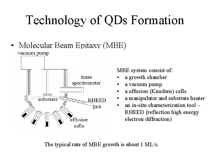
Technology of QDs Formation • Molecular Beam Epitaxy (MBE) MBE system consist of: • a growth chamber • a vacuum pump • a effusion (Knudsen) cells • a manipulator and substrate heater • an in-situ characterization tool – RHEED (reflection high energy electron diffraction) The typical rate of MBE growth is about 1 ML/s.

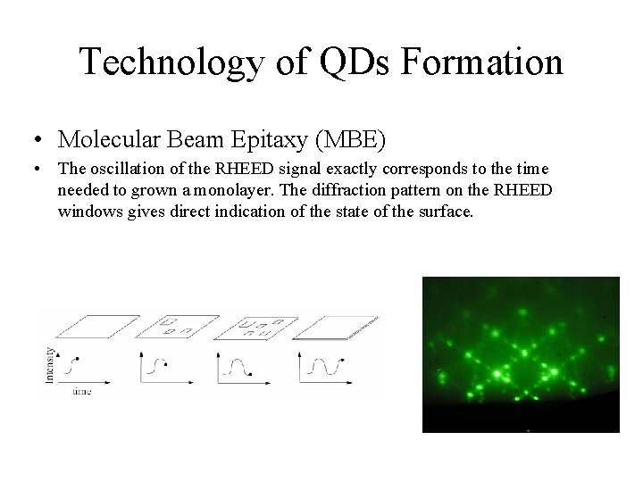
Technology of QDs Formation • Molecular Beam Epitaxy (MBE) • The oscillation of the RHEED signal exactly corresponds to the time needed to grown a monolayer. The diffraction pattern on the RHEED windows gives direct indication of the state of the surface.

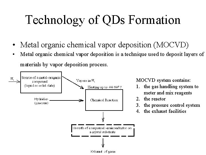
Technology of QDs Formation • Metal organic chemical vapor deposition (MOCVD) • Metal organic chemical vapor deposition is a technique used to deposit layers of materials by vapor deposition process. MOCVD system contains: 1. the gas handling system to meter and mix reagents 2. the reactor 3. the pressure control system 4. the exhaust facilities

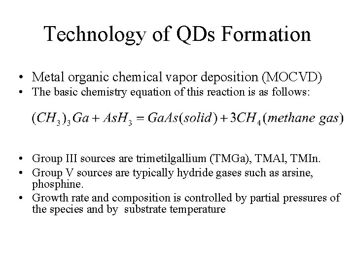
Technology of QDs Formation • Metal organic chemical vapor deposition (MOCVD) • The basic chemistry equation of this reaction is as follows: • Group III sources are trimetilgallium (TMGa), TMAl, TMIn. • Group V sources are typically hydride gases such as arsine, phosphine. • Growth rate and composition is controlled by partial pressures of the species and by substrate temperature

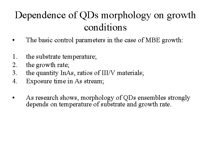
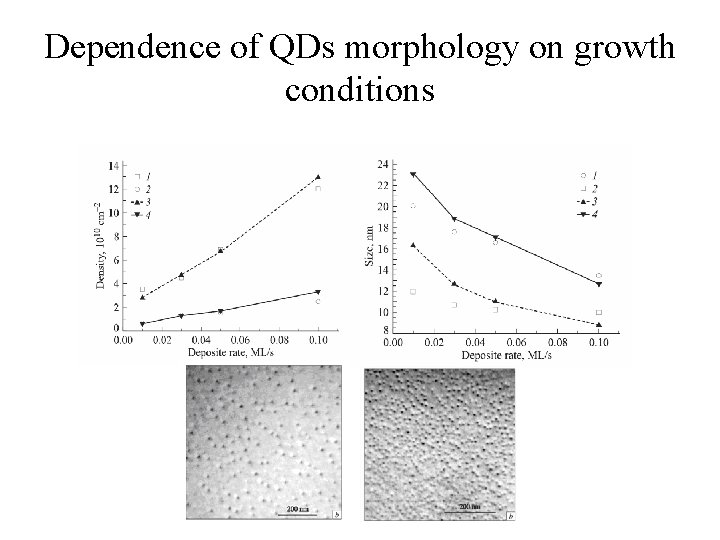
Dependence of QDs morphology on growth conditions • The basic control parameters in the case of MBE growth: 1. 2. 3. 4. the substrate temperature; the growth rate; the quantity In. As, ratios of III/V materials; Exposure time in As stream; • As research shows, morphology of QDs ensembles strongly depends on temperature of substrate and growth rate.

Dependence of QDs morphology on growth conditions

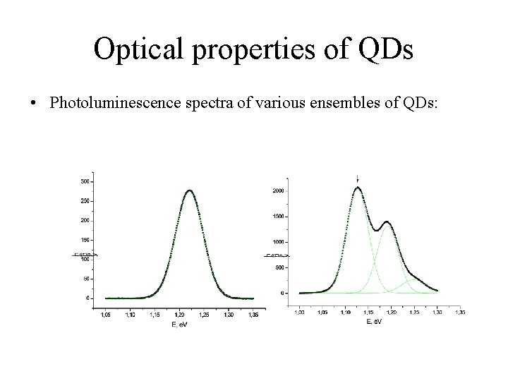
Optical properties of QDs • Photoluminescence spectra of various ensembles of QDs:

Optical properties of QDs • 1. The major processes which explain the temperature behavior of QDs PL-spectra: Thermal quenching of photoluminescence Thermal quenching is explained by thermal escape of carriers from QD into the barrier (or wetting layer) 2. “Red shifting” As experiment shows, at the temperature, when thermal quenching begins, we can see a following change: the maximum of PL line is shifting in the “red region”. Such behavior of PL spectrum is explained by thermal quenching of carriers and their redistribution between small and large QDs.

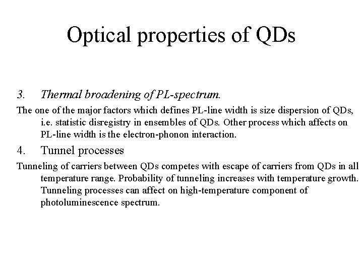
Optical properties of QDs 3. Thermal broadening of PL-spectrum. The one of the major factors which defines PL-line width is size dispersion of QDs, i. e. statistic disregistry in ensembles of QDs. Other process which affects on PL-line width is the electron-phonon interaction. 4. Tunnel processes Tunneling of carriers between QDs competes with escape of carriers from QDs in all temperature range. Probability of tunneling increases with temperature growth. Tunneling processes can affect on high-temperature component of photoluminescence spectrum.

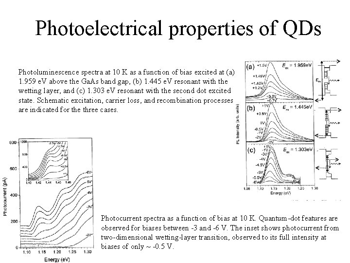
Photoelectrical properties of QDs Photoluminescence spectra at 10 K as a function of bias excited at (a) 1. 959 e. V above the Ga. As band gap, (b) 1. 445 e. V resonant with the wetting layer, and (c) 1. 303 e. V resonant with the second dot excited state. Schematic excitation, carrier loss, and recombination processes are indicated for the three cases. Photocurrent spectra as a function of bias at 10 K. Quantum-dot features are observed for biases between -3 and -6 V. The inset shows photocurrent from two-dimensional wetting-layer transition, observed to its full intensity at biases of only ~ -0. 5 V.

Semiconductor Quantum Dots Justin Galloway 2 -26 -07 Department of Materials Science & Engineering

Outline I. Introduction II. Effective Mass Model III. Reaction Techniques IV. Applications V. Conclusion

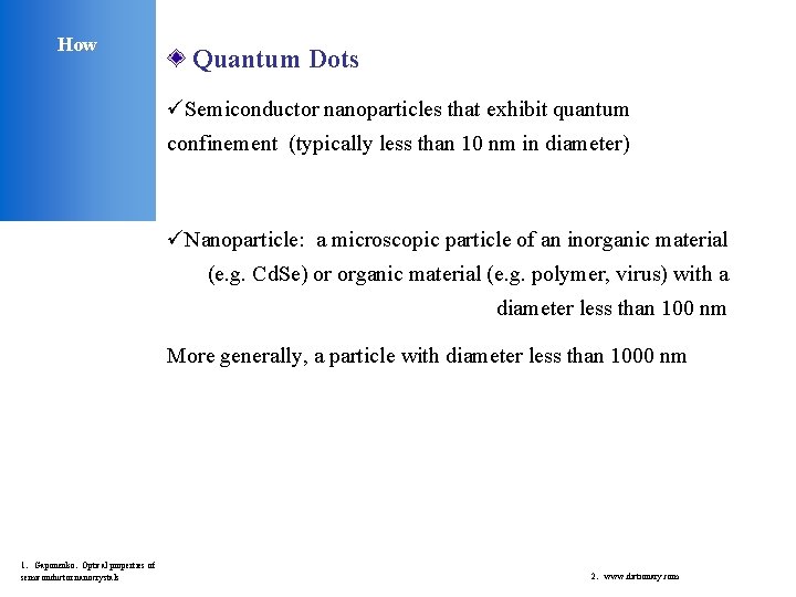
How Quantum Dots üSemiconductor nanoparticles that exhibit quantum confinement (typically less than 10 nm in diameter) üNanoparticle: a microscopic particle of an inorganic material (e. g. Cd. Se) or organic material (e. g. polymer, virus) with a diameter less than 100 nm More generally, a particle with diameter less than 1000 nm 1. Gaponenko. Optical properties of semiconductor nanocrystals 2. www. dictionary. com

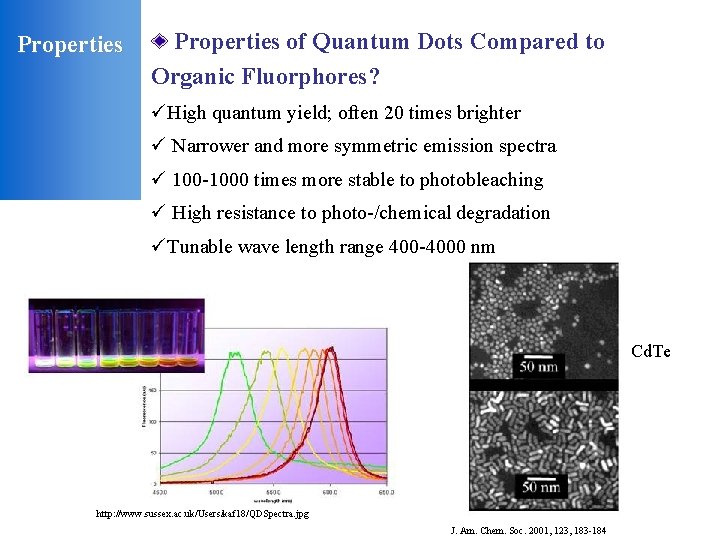
Properties of Quantum Dots Compared to Organic Fluorphores? üHigh quantum yield; often 20 times brighter ü Narrower and more symmetric emission spectra ü 100 -1000 times more stable to photobleaching ü High resistance to photo-/chemical degradation üTunable wave length range 400 -4000 nm Cd. Se Cd. Te http: //www. sussex. ac. uk/Users/kaf 18/QDSpectra. jpg J. Am. Chem. Soc. 2001, 123, 183 -184

Excitation in a Semiconductor üThe excitation of an electron from the valance band to the conduction band creates an electron hole pair Creation of an electron hole pair where h is the photon energy Band Gap (energy barrier) exciton: bound electron and hole pair usually associated with an electron trapped in a localized state in the band gap

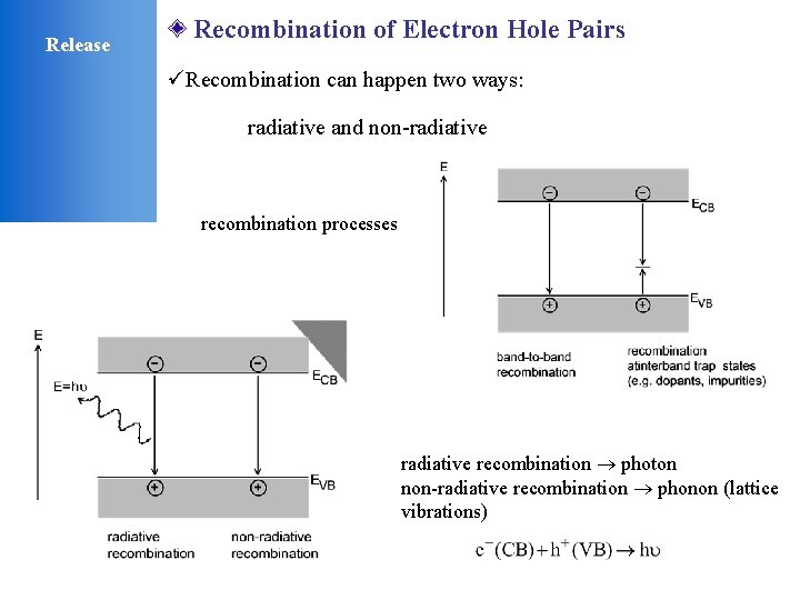
Release Recombination of Electron Hole Pairs üRecombination can happen two ways: radiative and non-radiative recombination processes radiative recombination photon non-radiative recombination phonon (lattice vibrations)

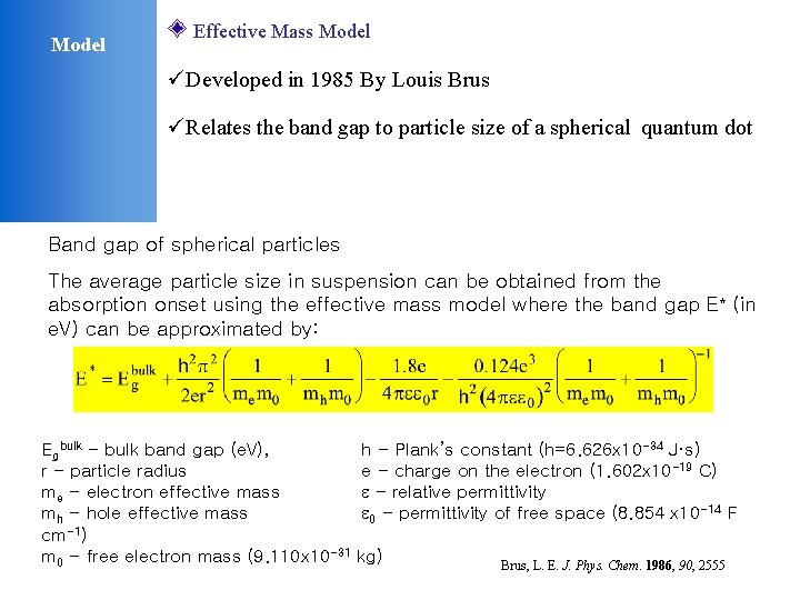
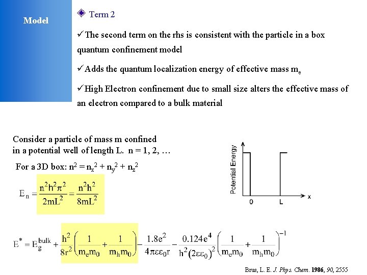
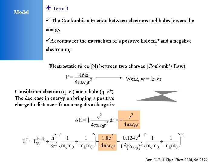
Model Effective Mass Model üDeveloped in 1985 By Louis Brus üRelates the band gap to particle size of a spherical quantum dot Band gap of spherical particles The average particle size in suspension can be obtained from the absorption onset using the effective mass model where the band gap E* (in e. V) can be approximated by: Egbulk - bulk band gap (e. V), r - particle radius me - electron effective mass mh - hole effective mass cm-1) m 0 - free electron mass (9. 110 x 10 -31 h - Plank’s constant (h=6. 626 x 10 -34 J·s) e - charge on the electron (1. 602 x 10 -19 C) - relative permittivity 0 - permittivity of free space (8. 854 x 10 -14 F kg) Brus, L. E. J. Phys. Chem. 1986, 90, 2555

Model Term 2 üThe second term on the rhs is consistent with the particle in a box quantum confinement model üAdds the quantum localization energy of effective mass me üHigh Electron confinement due to small size alters the effective mass of an electron compared to a bulk material Consider a particle of mass m confined in a potential well of length L. n = 1, 2, … For a 3 D box: n 2 = nx 2 + ny 2 + nz 2 Brus, L. E. J. Phys. Chem. 1986, 90, 2555

Model Term 3 ü The Coulombic attraction between electrons and holes lowers the energy üAccounts for the interaction of a positive hole me+ and a negative electron me. Electrostatic force (N) between two charges (Coulomb’s Law): Work, w = F·dr Consider an electron (q=e-) and a hole (q=e+) The decrease in energy on bringing a positive charge to distance r from a negative charge is: Brus, L. E. J. Phys. Chem. 1986, 90, 2555

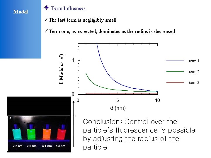
Term Influences üThe last term is negligibly small üTerm one, as expected, dominates as the radius is decreased Modulus Model Conclusion: Control over the particle’s fluorescence is possible by adjusting the radius of the particle

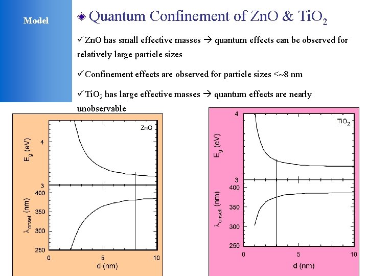
Model Quantum Confinement of Zn. O & Ti. O 2 üZn. O has small effective masses quantum effects can be observed for relatively large particle sizes üConfinement effects are observed for particle sizes <~8 nm üTi. O 2 has large effective masses quantum effects are nearly unobservable

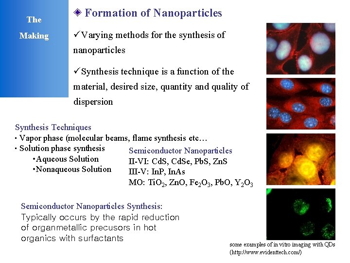
The Making Formation of Nanoparticles üVarying methods for the synthesis of nanoparticles üSynthesis technique is a function of the material, desired size, quantity and quality of dispersion Synthesis Techniques • Vapor phase (molecular beams, flame synthesis etc… • Solution phase synthesis Semiconductor Nanoparticles • Aqueous Solution II-VI: Cd. S, Cd. Se, Pb. S, Zn. S • Nonaqueous Solution III-V: In. P, In. As MO: Ti. O 2, Zn. O, Fe 2 O 3, Pb. O, Y 2 O 3 Semiconductor Nanoparticles Synthesis: Typically occurs by the rapid reduction of organmetallic precusors in hot organics with surfactants some examples of in vitro imaging with QDs (http: //www. evidenttech. com/)

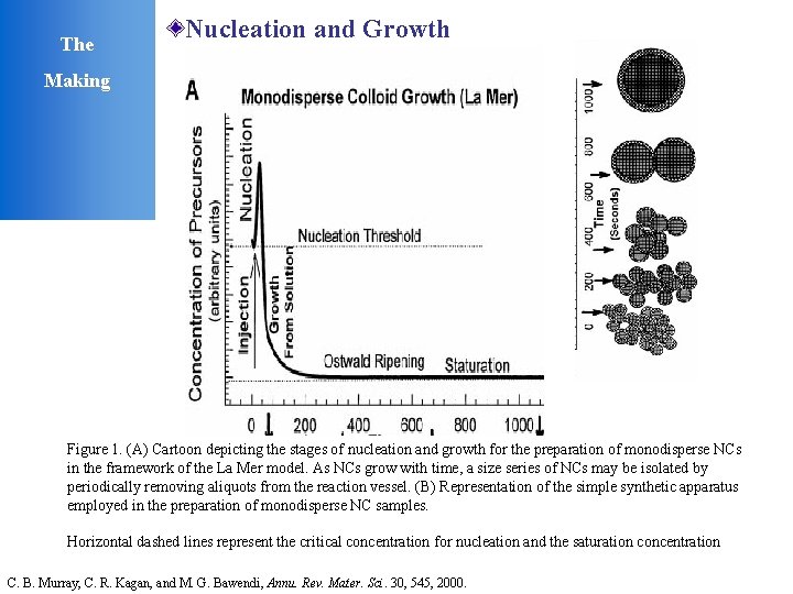
The Nucleation and Growth Making Figure 1. (A) Cartoon depicting the stages of nucleation and growth for the preparation of monodisperse NCs in the framework of the La Mer model. As NCs grow with time, a size series of NCs may be isolated by periodically removing aliquots from the reaction vessel. (B) Representation of the simple synthetic apparatus employed in the preparation of monodisperse NC samples. Horizontal dashed lines represent the critical concentration for nucleation and the saturation concentration C. B. Murray, C. R. Kagan, and M. G. Bawendi, Annu. Rev. Mater. Sci. 30, 545, 2000.

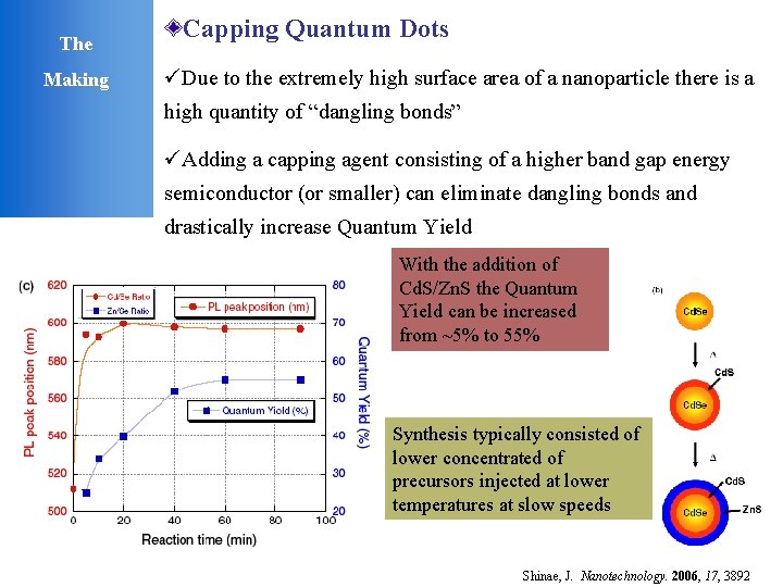
The Making Capping Quantum Dots üDue to the extremely high surface area of a nanoparticle there is a high quantity of “dangling bonds” üAdding a capping agent consisting of a higher band gap energy semiconductor (or smaller) can eliminate dangling bonds and drastically increase Quantum Yield With the addition of Cd. S/Zn. S the Quantum Yield can be increased from ~5% to 55% Synthesis typically consisted of lower concentrated of precursors injected at lower temperatures at slow speeds Shinae, J. Nanotechnology. 2006, 17, 3892

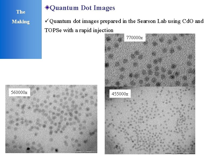
The Making Quantum Dot Images üQuantum dot images prepared in the Searson Lab using Cd. O and TOPSe with a rapid injection 770000 x 560000 x 455000 x

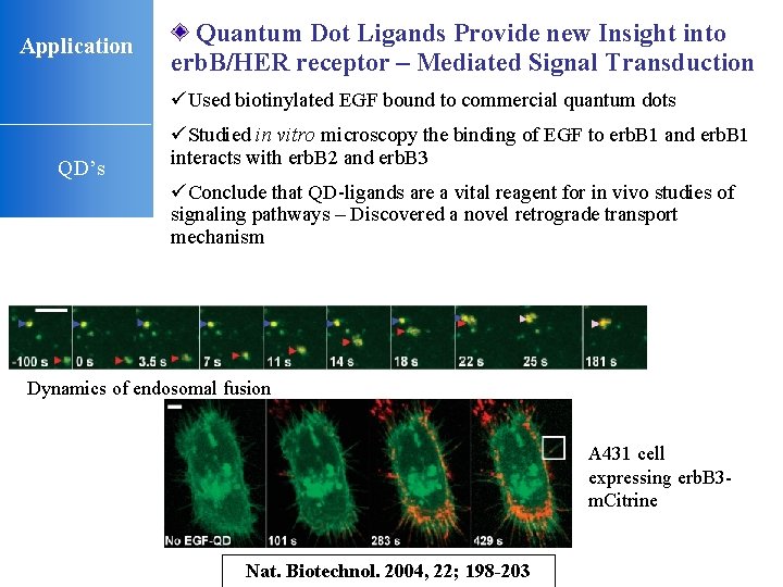
Application Quantum Dot Ligands Provide new Insight into erb. B/HER receptor – Mediated Signal Transduction üUsed biotinylated EGF bound to commercial quantum dots QD’s üStudied in vitro microscopy the binding of EGF to erb. B 1 and erb. B 1 interacts with erb. B 2 and erb. B 3 üConclude that QD-ligands are a vital reagent for in vivo studies of signaling pathways – Discovered a novel retrograde transport mechanism Dynamics of endosomal fusion A 431 cell expressing erb. B 3 m. Citrine Nat. Biotechnol. 2004, 22; 198 -203

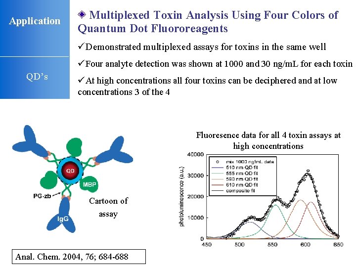
Application Multiplexed Toxin Analysis Using Four Colors of Quantum Dot Fluororeagents üDemonstrated multiplexed assays for toxins in the same well üFour analyte detection was shown at 1000 and 30 ng/m. L for each toxin QD’s üAt high concentrations all four toxins can be deciphered and at low concentrations 3 of the 4 Fluoresence data for all 4 toxin assays at high concentrations Cartoon of assay Anal. Chem. 2004, 76; 684 -688

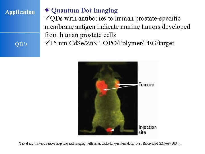
Application QD’s Quantum Dot Imaging üQDs with antibodies to human prostate-specific membrane antigen indicate murine tumors developed from human prostate cells ü 15 nm Cd. Se/Zn. S TOPO/Polymer/PEG/target Gao et al. , “In vivo cancer targeting and imaging with semiconductor quantum dots, ” Nat. Biotechnol. 22, 969 (2004).

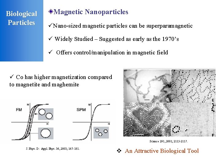
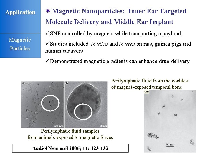
Biological Particles Magnetic Nanoparticles üNano-sized magnetic particles can be superparamagnetic ü Widely Studied – Suggested as early as the 1970’s ü Offers control/manipulation in magnetic field ü Co has higher magnetization compared to magnetite and maghemite Science 291, 2001; 2115 -2117. J. Phys. D: Appl. Phys. 36, 2003; 167 -181. v An Attractive Biological Tool

Application Magnetic Nanoparticles: Inner Ear Targeted Molecule Delivery and Middle Ear Implant üSNP controlled by magnets while transporting a payload Magnetic Particles üStudies included in vitro and in vivo on rats, guinea pigs and human cadavers üDemonstrated magnetic gradients can enhance drug delivery Perilymphatic fluid from the cochlea of magnet-exposed temporal bone Perilymphatic fluid samples from animals exposed to magnetic forces Audiol Neurotol 2006; 11: 123 -133

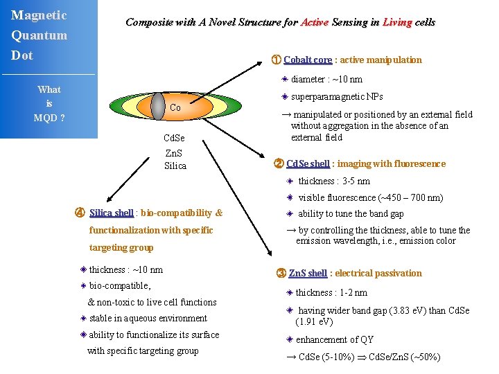
Magnetic Quantum Dot Composite with A Novel Structure for Active Sensing in Living cells ① Cobalt core : active manipulation diameter : ~10 nm What is MQD ? Co Cd. Se Zn. S Silica superparamagnetic NPs → manipulated or positioned by an external field without aggregation in the absence of an external field ② Cd. Se shell : imaging with fluorescence thickness : 3 -5 nm visible fluorescence (~450 – 700 nm) ④ Silica shell : bio-compatibility & functionalization with specific targeting group thickness : ~10 nm bio-compatible, & non-toxic to live cell functions ability to tune the band gap → by controlling the thickness, able to tune the emission wavelength, i. e. , emission color ③ Zn. S shell : electrical passivation thickness : 1 -2 nm stable in aqueous environment having wider band gap (3. 83 e. V) than Cd. Se (1. 91 e. V) ability to functionalize its surface enhancement of QY with specific targeting group → Cd. Se (5 -10%) Cd. Se/Zn. S (~50%)

Rap-Up Conclusions ØThe effective mass model give an excellent approximation of the size dependence of electronic properties of a quantum dot ØRecent synthesis advances have shown many quantum dot reactions to be robust, cheap, and safe then previously thought ØQuantum dots offer wide range electronic properties that make them an attractive tool for biological and medical work ØMQD’s improve afford in vivo manipulation expanded the applicability of quantum dots

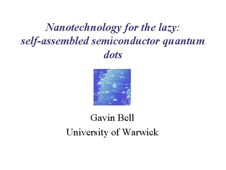
Nanotechnology for the lazy: self-assembled semiconductor quantum dots Gavin Bell University of Warwick

Outline • Semiconductor quantum dots – what, why? – Artificial versus self-assembled (SAQD) • In. As/Ga. As SAQDs – Strained heteroepitaxy in MBE • Analysing and controlling SAQD growth – STM-MBE versus “STMBE” – SEM, TEM, CAFM

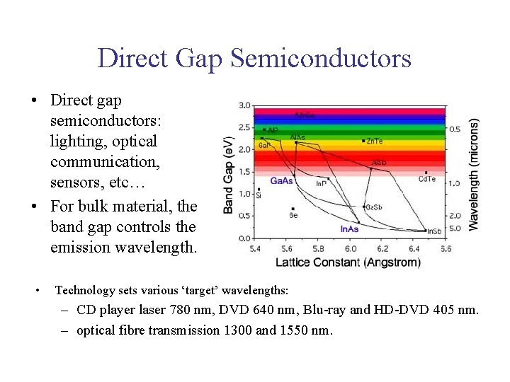
Direct Gap Semiconductors • Direct gap semiconductors: lighting, optical communication, sensors, etc… • For bulk material, the band gap controls the emission wavelength. • Technology sets various ‘target’ wavelengths: – CD player laser 780 nm, DVD 640 nm, Blu-ray and HD-DVD 405 nm. – optical fibre transmission 1300 and 1550 nm.

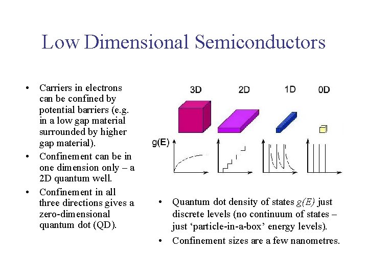
Low Dimensional Semiconductors • Carriers in electrons can be confined by potential barriers (e. g. in a low gap material surrounded by higher gap material). • Confinement can be in one dimension only – a 2 D quantum well. • Confinement in all three directions gives a zero-dimensional quantum dot (QD). • Quantum dot density of states g(E) just discrete levels (no continuum of states – just ‘particle-in-a-box’ energy levels). • Confinement sizes are a few nanometres.

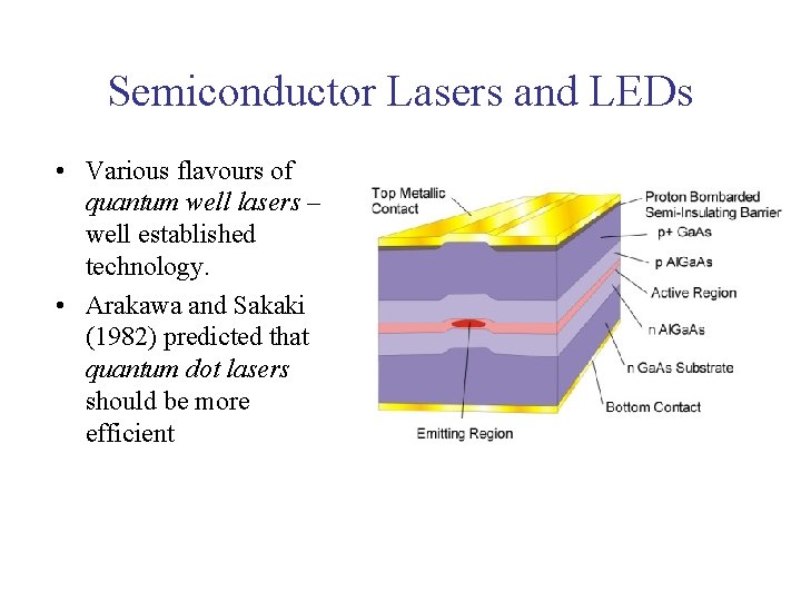
Semiconductor Lasers and LEDs • Various flavours of quantum well lasers – well established technology. • Arakawa and Sakaki (1982) predicted that quantum dot lasers should be more efficient

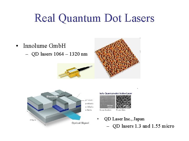
Real Quantum Dot Lasers • Innolume Gmb. H – QD lasers 1064 – 1320 nm • QD Laser Inc. , Japan – QD lasers 1. 3 and 1. 55 micro

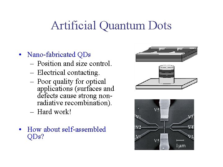
Artificial Quantum Dots • Nano-fabricated QDs – Position and size control. – Electrical contacting. – Poor quality for optical applications (surfaces and defects cause strong nonradiative recombination). – Hard work! • How about self-assembled QDs?

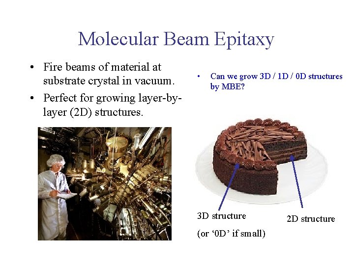
Molecular Beam Epitaxy • Fire beams of material at substrate crystal in vacuum. • Perfect for growing layer-bylayer (2 D) structures. • Can we grow 3 D / 1 D / 0 D structures by MBE? 3 D structure (or ‘ 0 D’ if small) 2 D structure

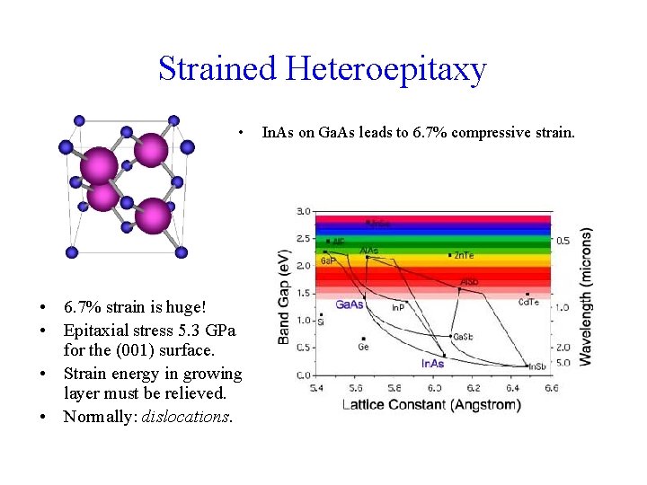
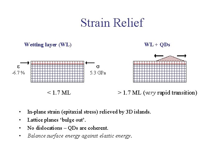
Strained Heteroepitaxy • • 6. 7% strain is huge! • Epitaxial stress 5. 3 GPa for the (001) surface. • Strain energy in growing layer must be relieved. • Normally: dislocations. In. As on Ga. As leads to 6. 7% compressive strain.

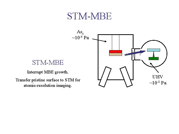
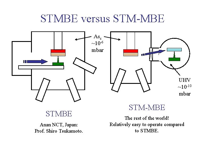
STM-MBE Asx ~10 -4 Pa STM-MBE Interrupt MBE growth. Transfer pristine surface to STM for atomic-resolution imaging. UHV ~10 -8 Pa

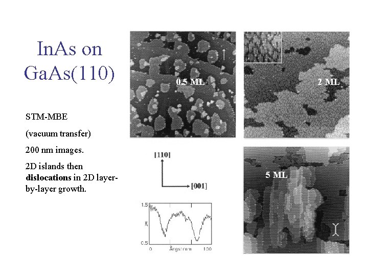
0. 5 ML In. As on Ga. As(110) 0. 5 ML 2 ML STM-MBE (vacuum transfer) 200 nm images. 2 D islands then dislocations in 2 D layerby-layer growth. 5 ML

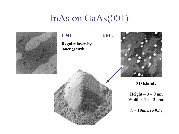
In. As on Ga. As(001) 1 ML 2 ML Regular layer-bylayer growth 3 D islands Height ~ 3 – 8 nm Width ~ 10 – 20 nm l ~ 10 nm, so 0 D?

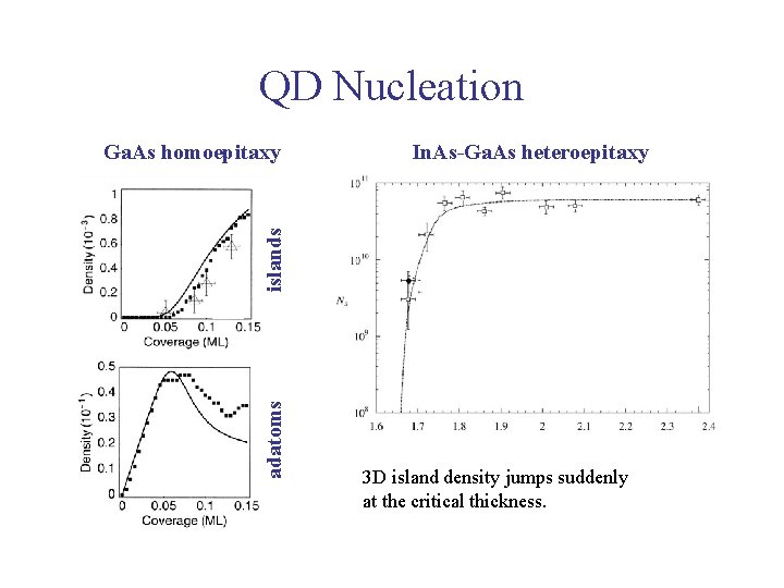
Strain Relief Wetting layer (WL) WL + QDs ε σ -6. 7 % 5. 3 GPa < 1. 7 ML • • > 1. 7 ML (very rapid transition) In-plane strain (epitaxial stress) relieved by 3 D islands. Lattice planes ‘bulge out’. No dislocations – QDs are coherent. Balance surface energy against elastic energy.

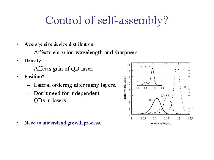
Control of self-assembly? • Average size & size distribution. – Affects emission wavelength and sharpness. • Density. – Affects gain of QD laser. • Position? – Lateral ordering after many layers. – Don’t need for independent QDs in lasers. • Need to understand growth process.

QD Nucleation In. As-Ga. As heteroepitaxy adatoms islands Ga. As homoepitaxy 3 D island density jumps suddenly at the critical thickness.

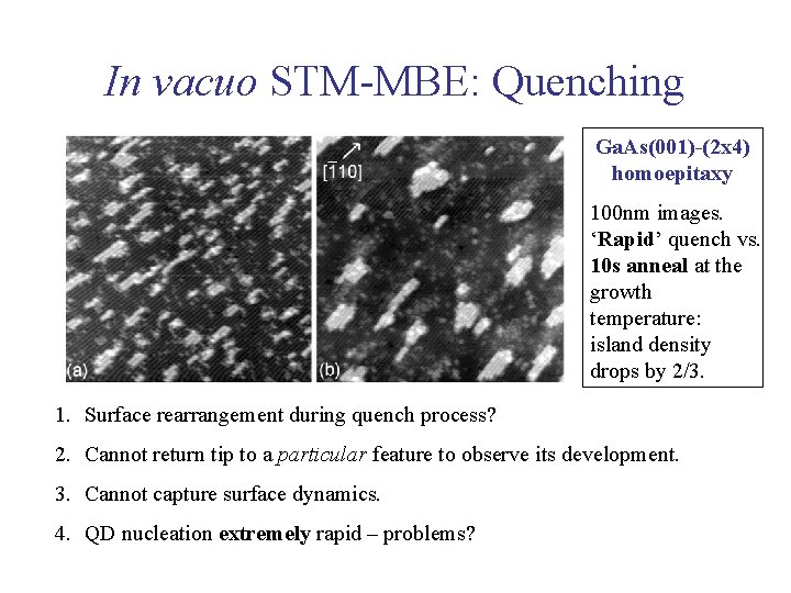
In vacuo STM-MBE: Quenching Ga. As(001)-(2 x 4) homoepitaxy 100 nm images. ‘Rapid’ quench vs. 10 s anneal at the growth temperature: island density drops by 2/3. 1. Surface rearrangement during quench process? 2. Cannot return tip to a particular feature to observe its development. 3. Cannot capture surface dynamics. 4. QD nucleation extremely rapid – problems?

STMBE versus STM-MBE Asx ~10 -6 mbar UHV ~10 -10 mbar STMBE Anan NCT, Japan: Prof. Shiro Tsukamoto. STM-MBE The rest of the world! Relatively easy to operate compared to STMBE.

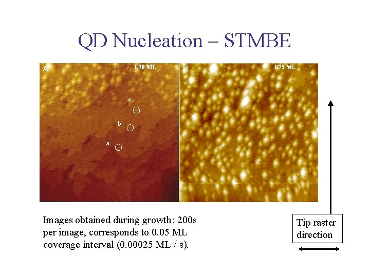
QD Nucleation – STMBE 1. 70 ML A B 1. 75 ML c b a Images obtained during growth: 200 s per image, corresponds to 0. 05 ML coverage interval (0. 00025 ML / s). Tip raster direction

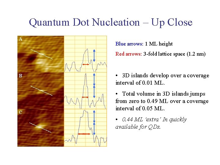
Quantum Dot Nucleation – Up Close A Blue arrows: 1 ML height Red arrows: 3 -fold lattice space (1. 2 nm) B C • 3 D islands develop over a coverage interval of 0. 01 ML. • Total volume in 3 D islands jumps from zero to 0. 49 ML over a coverage interval of 0. 05 ML. • 0. 44 ML ‘extra’ In quickly available for QDs.

Wetting Layer Growth • STMBE ‘movie’ of WL growth. • Observe normal step-flow growth. – Fill in pits. – Terrace advances. – Island grows and joins up with terrace. • Each frame 200 s, 0. 05 ML. • Measure area of ‘new’ terrace developed in each frame. – Can’t do this with STM-MBE. • Amount of new terrace always less than amount of deposited In. As. • About 0. 5 ML In available for rapid QD nucleation as mobile, weakly bound adatoms.

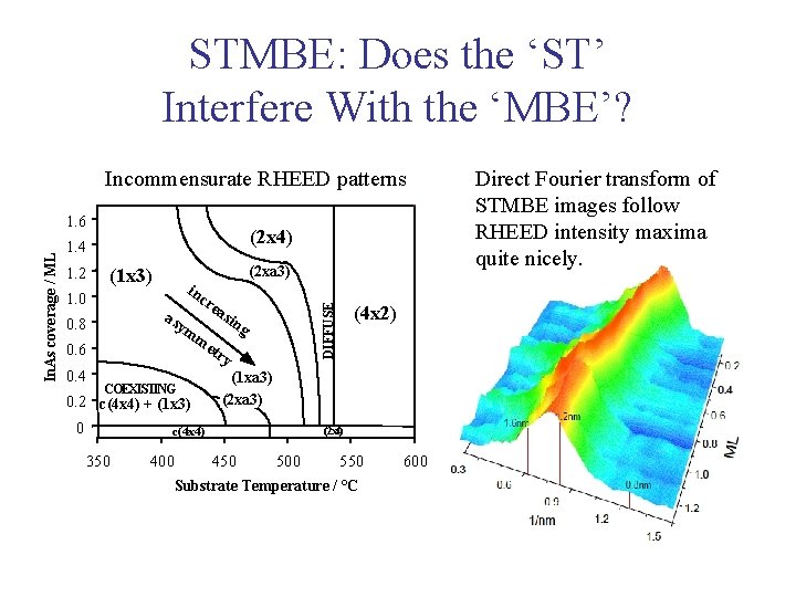
STMBE: Does the ‘ST’ Interfere With the ‘MBE’? Incommensurate RHEED patterns (2 x 4) 1. 4 1. 2 (1 x 3) 1. 0 in cr as ea ym me 0. 8 sin g try 0. 6 0. 4 (2 xa 3) COEXISTING 0. 2 c(4 x 4) + (1 x 3) 0 c(4 x 4) 350 400 (4 x 2) DIFFUSE In. As coverage / ML 1. 6 (1 xa 3) (2 xa 3) 2 (2 x 4) 450 500 550 Substrate Temperature / °C 600 Direct Fourier transform of STMBE images follow RHEED intensity maxima quite nicely.

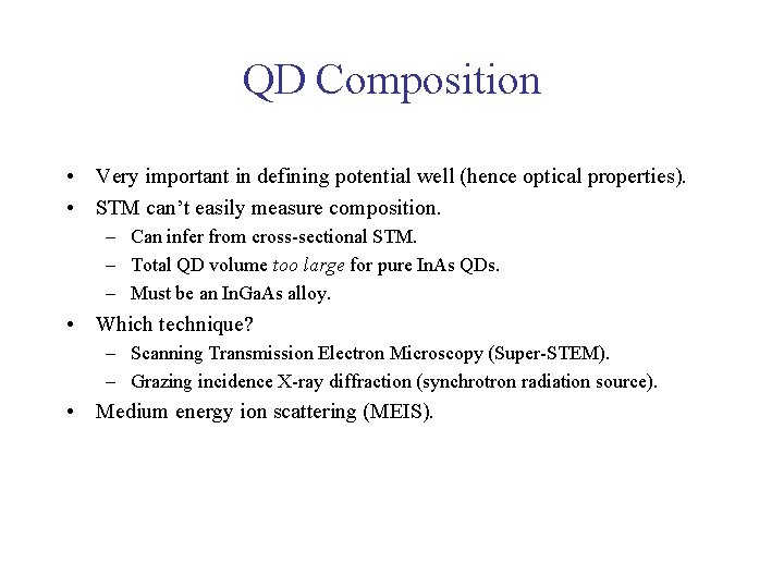
QD Composition • Very important in defining potential well (hence optical properties). • STM can’t easily measure composition. – Can infer from cross-sectional STM. – Total QD volume too large for pure In. As QDs. – Must be an In. Ga. As alloy. • Which technique? – Scanning Transmission Electron Microscopy (Super-STEM). – Grazing incidence X-ray diffraction (synchrotron radiation source). • Medium energy ion scattering (MEIS).

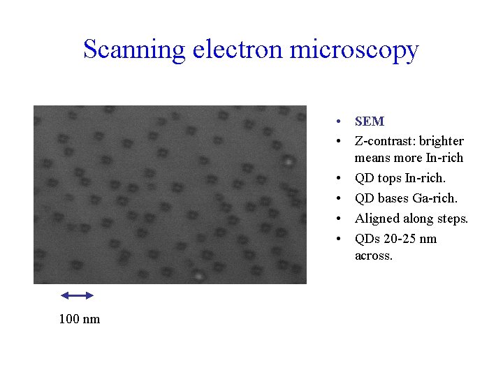
Scanning electron microscopy • SEM • Z-contrast: brighter means more In-rich • QD tops In-rich. • QD bases Ga-rich. • Aligned along steps. • QDs 20 -25 nm across. 100 nm

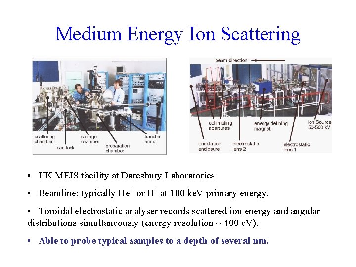
Medium Energy Ion Scattering • UK MEIS facility at Daresbury Laboratories. • Beamline: typically He+ or H+ at 100 ke. V primary energy. • Toroidal electrostatic analyser records scattered ion energy and angular distributions simultaneously (energy resolution ~ 400 e. V). • Able to probe typical samples to a depth of several nm.

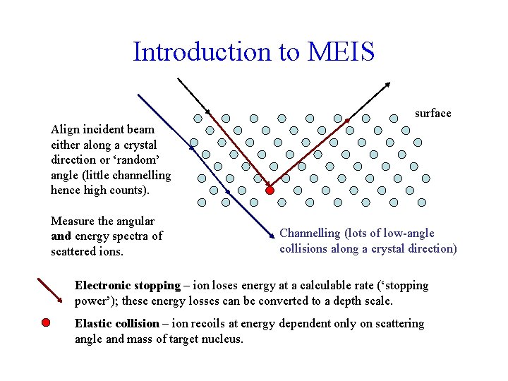
Introduction to MEIS surface Align incident beam either along a crystal direction or ‘random’ angle (little channelling hence high counts). Measure the angular and energy spectra of scattered ions. Channelling (lots of low-angle collisions along a crystal direction) Electronic stopping – ion loses energy at a calculable rate (‘stopping power’); these energy losses can be converted to a depth scale. Elastic collision – ion recoils at energy dependent only on scattering angle and mass of target nucleus.

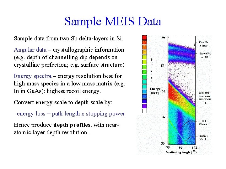
Sample MEIS Data Sample data from two Sb delta-layers in Si. Angular data – crystallographic information (e. g. depth of channelling dip depends on crystalline perfection; e. g. surface structure) Energy spectra – energy resolution best for high mass species in a low mass matrix (e. g. In in Ga. As): highest recoil energy. Convert energy scale to depth scale by: energy loss = path length x stopping power Hence produce depth profiles, with nearatomic layer depth resolution.
![QD Energy Spectra Channelled spectra 110 in and normal out very similar for uncapped QD Energy Spectra Channelled spectra, [110] in and normal out, very similar for uncapped](https://slidetodoc.com/presentation_image_h/e608ec740f949154eddf4b999cc5ac42/image-83.jpg)
QD Energy Spectra Channelled spectra, [110] in and normal out, very similar for uncapped (red) and 1 nm Ga. As cap (partially capped QDs). Thicker Ga. As cap (5 nm): In signal merges into Ga. As. Concentrate on uncapped QDs.

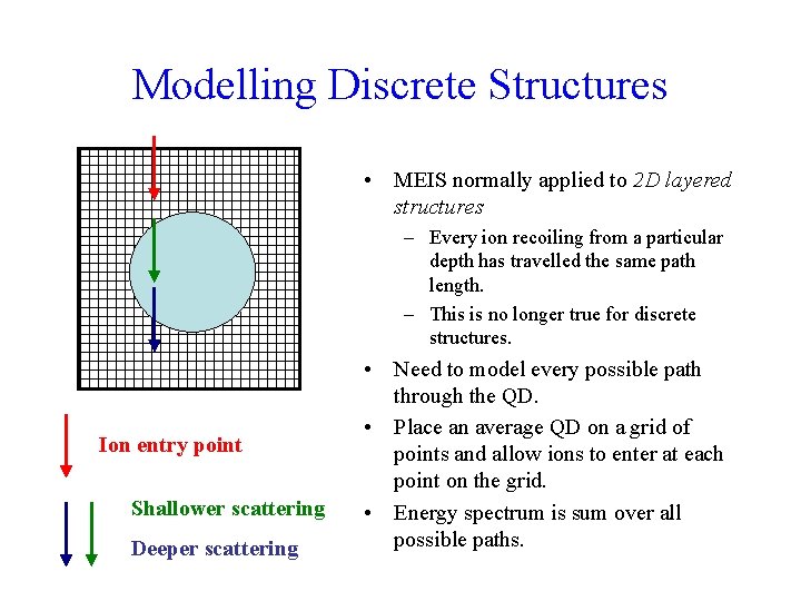
Modelling Discrete Structures • MEIS normally applied to 2 D layered structures – Every ion recoiling from a particular depth has travelled the same path length. – This is no longer true for discrete structures. Ion entry point Shallower scattering Deeper scattering • Need to model every possible path through the QD. • Place an average QD on a grid of points and allow ions to enter at each point on the grid. • Energy spectrum is sum over all possible paths.

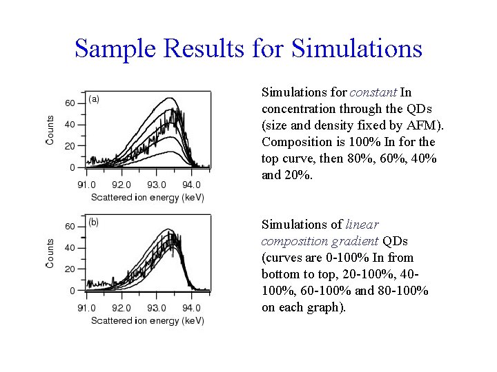
Sample Results for Simulations for constant In concentration through the QDs (size and density fixed by AFM). Composition is 100% In for the top curve, then 80%, 60%, 40% and 20%. Simulations of linear composition gradient QDs (curves are 0 -100% In from bottom to top, 20 -100%, 40100%, 60 -100% and 80 -100% on each graph).

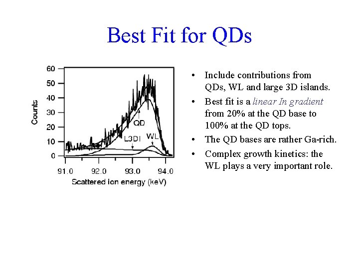
Best Fit for QDs • Include contributions from QDs, WL and large 3 D islands. • Best fit is a linear In gradient from 20% at the QD base to 100% at the QD tops. • The QD bases are rather Ga-rich. • Complex growth kinetics: the WL plays a very important role.

Conclusions • Semiconductor quantum dots. – Self-assembled versus fabricated. • In. As-Ga. As QDs easy to grow by MBE. – Possible to tailor to important wavelengths (e. g. 1300 nm). • Study growth in detail with STM. – STMBE ‘movies’ versus STM-MBE ‘snapshots’. – Growth kinetics not fully understood. • Study composition of discrete nanostructures with medium energy ion scattering (MEIS).