Threedimensional quantum heterostructures quantum wells wires and dots

- Slides: 15

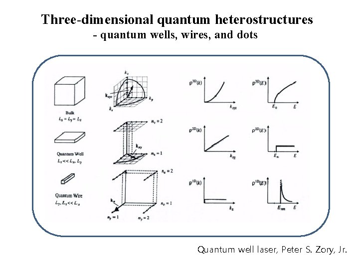
Three-dimensional quantum heterostructures - quantum wells, wires, and dots Quantum well laser, Peter S. Zory, Jr.

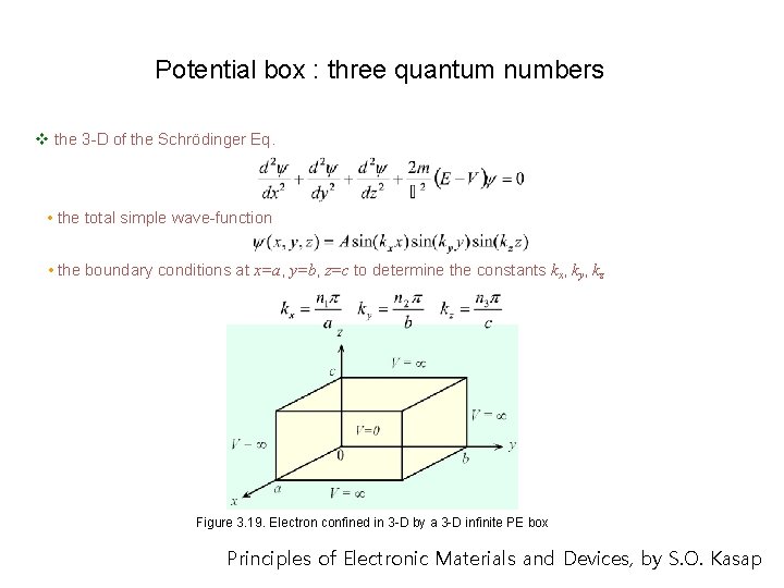
Potential box : three quantum numbers v the 3 -D of the Schrödinger Eq. • the total simple wave-function • the boundary conditions at x=a, y=b, z=c to determine the constants kx, ky, kz Figure 3. 19. Electron confined in 3 -D by a 3 -D infinite PE box Principles of Electronic Materials and Devices, by S. O. Kasap

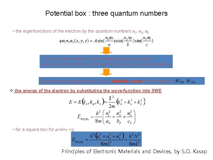
Potential box : three quantum numbers • the eigenfunctions of the electron by the quantum numbers n 1, n 2, n 3 The products of infinite 1 -D PE well-type wave-functions, one for each dimension, and each has its own quantum number n Each possible eigenfunction can be labeled a state for the electron v the energy of the electron by substituting the wave-function into SWE • for a square box for a=b=c =L Principles of Electronic Materials and Devices, by S. O. Kasap

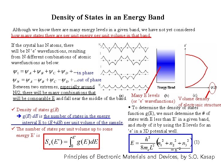
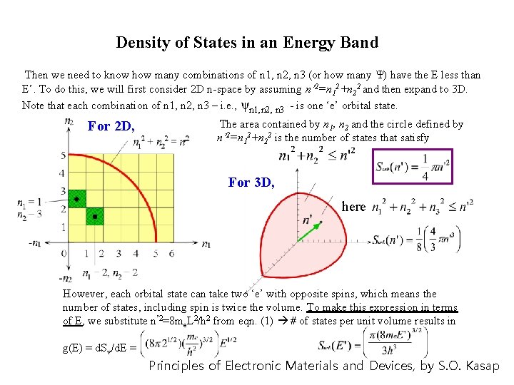
4. 5 Density of States in an Energy Band Although we know there are many energy levels in a given band, we have not yet considered how many states there are per unit energy per unit volume in that band. If the crystal has N atoms, there will be N ‘e’ wavefunctions, resulting from N different combinations of atomic wavefunctions as below. in phase out of phase Between two extremes, especially around N/2, there will be many combinations that Many E levels will be comparable E and fall near the middle of the band. (or ‘e’ wavefunctions) Volume density of electronic structure w To determine the density of states ü Density of states g(E) function g(E), we must determine the # of g(E) d. E is the number of states in the energy states with E less than E’ in a given band, interval E to (E+d. E) per unit volume of the sample. and study of it by using the E levels for an ü The number of states per unit volume up to some ‘e’ in a 3 D potential well. energy E’ is (1) = n’ 2 Principles of Electronic Materials and Devices, by S. O. Kasap

4. 5 Density of States in an Energy Band Then we need to know how many combinations of n 1, n 2, n 3 (or how many Ψ) have the E less than E’. To do this, we will first consider 2 D n-space by assuming n’ 2=n 12+n 22 and then expand to 3 D. Note that each combination of n 1, n 2, n 3 – i. e. , ψn 1, n 2, n 3 - is one ‘e’ orbital state. For 2 D, The area contained by n 1, n 2 and the circle defined by n’ 2=n 12+n 22 is the number of states that satisfy For 3 D, here However, each orbital state can take two ‘e’ with opposite spins, which means the number of states, including spin is twice the volume. To make this expression in terms of E, we substitute n’ 2=8 me. L 2/h 2 from eqn. (1) # of states per unit volume results in g(E) = d. Sv/d. E = Principles of Electronic Materials and Devices, by S. O. Kasap

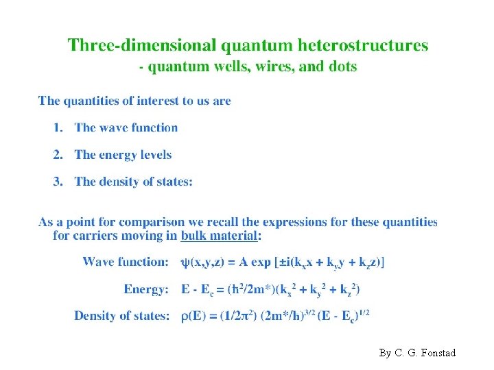
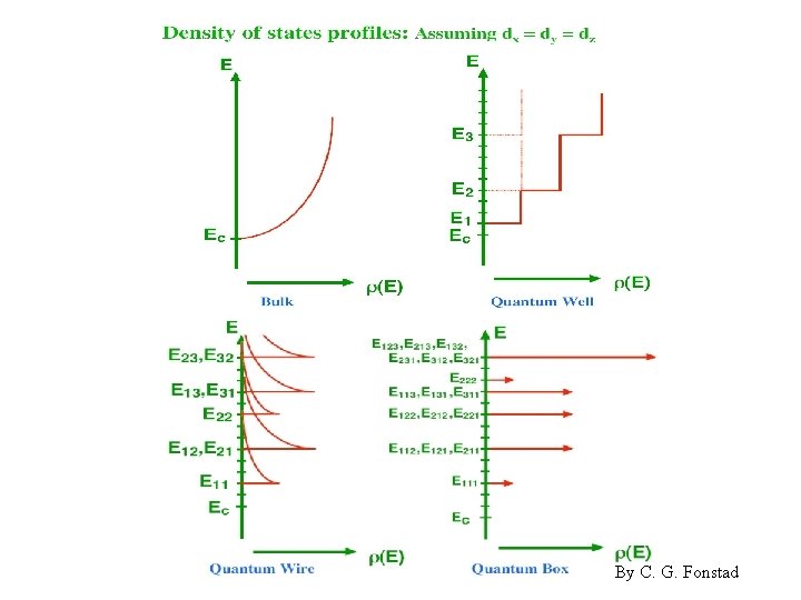
By C. G. Fonstad

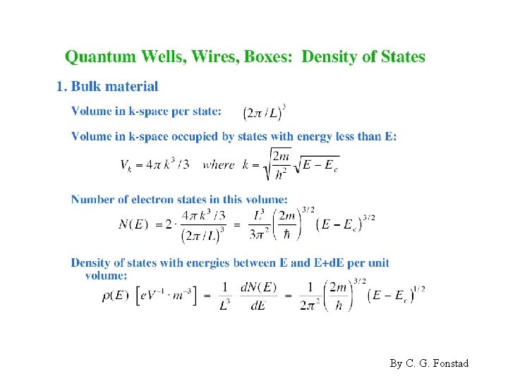
By C. G. Fonstad

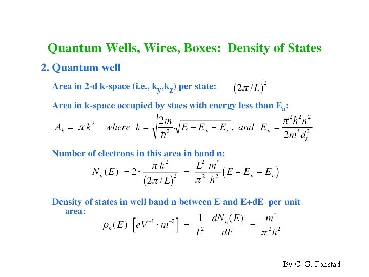
By C. G. Fonstad

By C. G. Fonstad

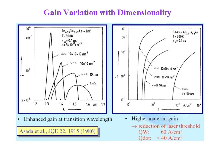
Gain Variation with Dimensionality

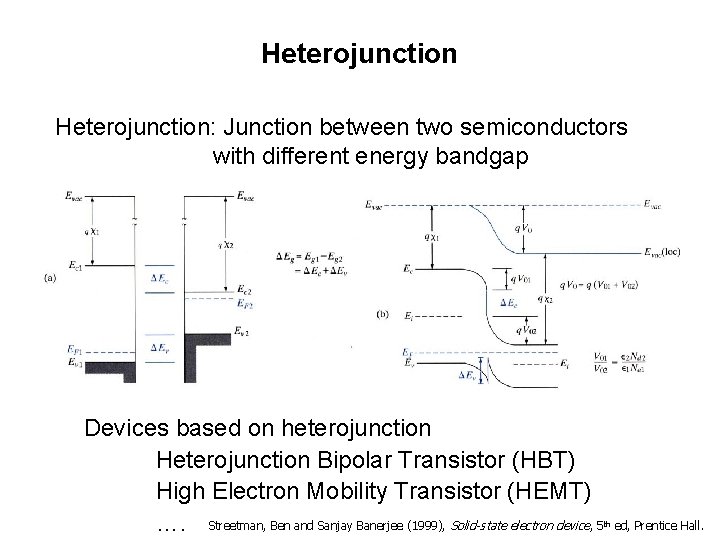
Heterojunction: Junction between two semiconductors with different energy bandgap Devices based on heterojunction Heterojunction Bipolar Transistor (HBT) High Electron Mobility Transistor (HEMT) …. Streetman, Ben and Sanjay Banerjee (1999), Solid-state electron device, 5 th ed, Prentice Hall.

Device Issues: - Ohmic Contacts

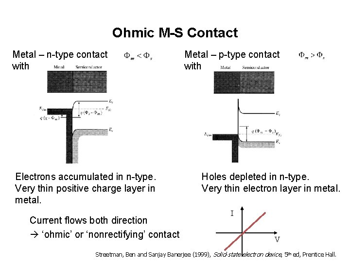
Ohmic M-S Contact Metal – n-type contact with Electrons accumulated in n-type. Very thin positive charge layer in metal. Current flows both direction ‘ohmic’ or ‘nonrectifying’ contact Metal – p-type contact with Holes depleted in n-type. Very thin electron layer in metal. I V Streetman, Ben and Sanjay Banerjee (1999), Solid-state electron device , 5 th ed, Prentice Hall.

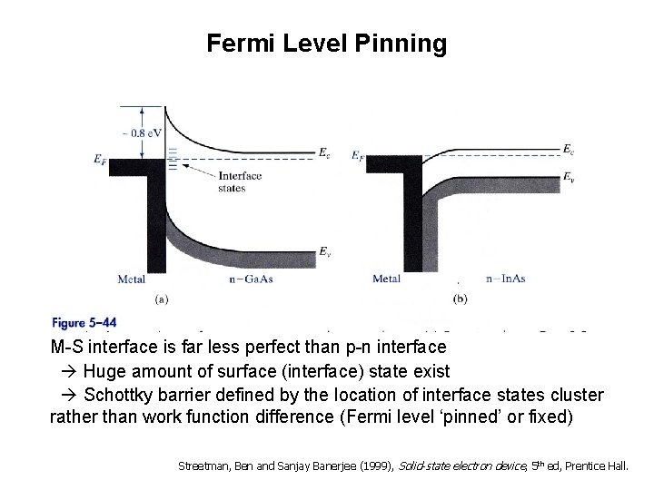
Fermi Level Pinning M-S interface is far less perfect than p-n interface Huge amount of surface (interface) state exist Schottky barrier defined by the location of interface states cluster rather than work function difference (Fermi level ‘pinned’ or fixed) Streetman, Ben and Sanjay Banerjee (1999), Solid-state electron device , 5 th ed, Prentice Hall.

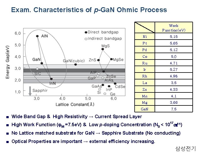
Exam. Characteristics of p-Ga. N Ohmic Process Work Function(e. V) Ni 5. 15 Pt 5. 65 Pd 5. 12 Co 5. 0 Ru 4. 71 Ir 5. 27 Rh 4. 98 La 3. 5 Zn 4. 33 Mn 4. 1 Mg 3. 66 Ga. N 7. 5 ■ Wide Band Gap & High Resistivity → Current Spread Layer ■ High Work Function (φM =7. 5 e. V) & Low p-doping Concentration (ND < 1017㎤-1) ■ No Lattice matched substrate for Ga. N → Sapphire Substrate (No conducting) ■ Optical Properties are important → external efficiency increasing. 삼성전기