Platforms I Dezs Sima 2011 Ver 1 1





![2. 3. 2. 2 Memory type (14) Green and ultra-low power memories- Examples [13] 2. 3. 2. 2 Memory type (14) Green and ultra-low power memories- Examples [13]](https://slidetodoc.com/presentation_image_h2/63bf6bfb565824c352f6768862af55ac/image-83.jpg)
![2. 3. 2. 2 Memory type (17) The architecture of FB-DIMM memories [19] 2. 3. 2. 2 Memory type (17) The architecture of FB-DIMM memories [19]](https://slidetodoc.com/presentation_image_h2/63bf6bfb565824c352f6768862af55ac/image-86.jpg)
![2. 3. 2. 2 Memory type (26) Latency [22] • Due to their additional 2. 3. 2. 2 Memory type (26) Latency [22] • Due to their additional](https://slidetodoc.com/presentation_image_h2/63bf6bfb565824c352f6768862af55ac/image-95.jpg)


![5. References (1) [1]: Wikipedia: Centrino, http: //en. wikipedia. org/wiki/Centrino [2]: Industry Uniting Around 5. References (1) [1]: Wikipedia: Centrino, http: //en. wikipedia. org/wiki/Centrino [2]: Industry Uniting Around](https://slidetodoc.com/presentation_image_h2/63bf6bfb565824c352f6768862af55ac/image-117.jpg)
![5. References (2) [11]: Ng P. K. , “High End Desktop Platform Design Overview 5. References (2) [11]: Ng P. K. , “High End Desktop Platform Design Overview](https://slidetodoc.com/presentation_image_h2/63bf6bfb565824c352f6768862af55ac/image-118.jpg)
![5. References (3) [20]: „Introducing FB-DIMM Memory: Birth of Serial RAM? , ” PCStats, 5. References (3) [20]: „Introducing FB-DIMM Memory: Birth of Serial RAM? , ” PCStats,](https://slidetodoc.com/presentation_image_h2/63bf6bfb565824c352f6768862af55ac/image-119.jpg)
- Slides: 119

Platforms I. Dezső Sima 2011 (Ver. 1. 1) Sima Dezső, 2011

Contents • 1. Introduction to platforms • 2. Main components of platforms • 3. Platform architectures • 4. Memory subsystem design considerations • 5. References

1. Introduction to platforms • 1. 1. The notion of platform • 1. 2. Description of particular platforms • 1. 3. Representation forms of platforms • 1. 4. Compatibility of platform components

1. 1. The notion of platform

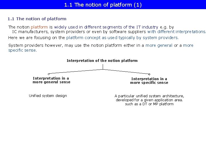
1. 1 The notion of platform (1) 1. 1 The notion of platform The notion platform is widely used in different segments of the IT industry e. g. by IC manufacturers, system providers or even by software suppliers with different interpretations. Here we are focusing on the platform concept as used typically by system providers. System providers however, may use the notion platform either in a more general or a more specific sense. Interpretation of the notion platform Interpretation in a more general sense Unified system design Interpretation in a more specific sense A particular unified system architecture, developed for a given application area. such as a DT or MP platform

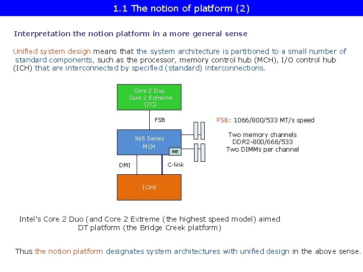
1. 1 The notion of platform (2) Interpretation the notion platform in a more general sense Unified system design means that the system architecture is partitioned to a small number of standard components, such as the processor, memory control hub (MCH), I/O control hub (ICH) that are interconnected by specified (standard) interconnections. Core 2 Duo Core 2 Extreme (2 C) FSB 965 Series MCH FSB: 1066/800/533 MT/s speed ME Two memory channels DDR 2 -800/666/533 Two DIMMs per channel C-link DMI ICH 8 Intel’s Core 2 Duo (and Core 2 Extreme (the highest speed model) aimed DT platform (the Bridge Creek platform) Thus the notion platform designates system architectures with unified design in the above sense.

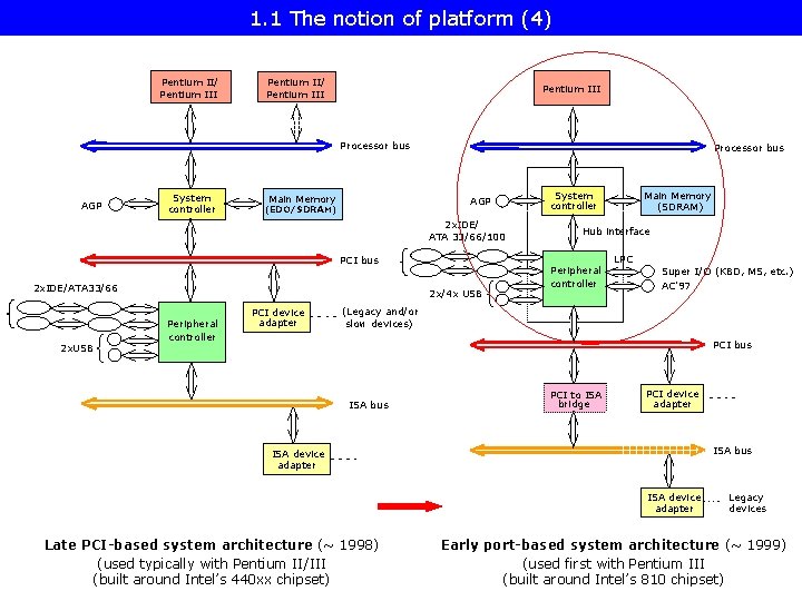
1. 1 The notion of platform (3) Remark The need for a unified system design, called platform design, arose in the PC industry in the time when PCI-based system designs were substituted by port based system designs, about 1998 -1999.

1. 1 The notion of platform (4) Pentium II/ Pentium III Processor bus AGP System controller Main Memory Processor bus AGP (EDO/SDRAM) 2 x. IDE/ ATA 33/66/100 PCI bus 2 x. IDE/ATA 33/66 2 x. USB 2 x/4 x USB Peripheral controller PCI device adapter Main Memory (SDRAM) System controller Hub interface Peripheral controller LPC Super I/O (KBD, MS, etc. ) AC'97 (Legacy and/or slow devices) PCI bus ISA bus PCI to ISA bridge PCI device adapter ISA bus ISA device adapter Late PCI-based system architecture (~ 1998) (used typically with Pentium II/III (built around Intel’s 440 xx chipset) Legacy devices Early port-based system architecture (~ 1999) (used first with Pentium III (built around Intel’s 810 chipset)

1. 1 The notion of platform (5) The primary goals of introducing unified system designs are • to minimize design rework while moving from one processor generation to the next and • to stabilize interfaces for server and desktop designs [2] • to shorten the time to market.

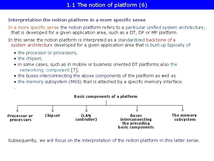
1. 1 The notion of platform (6) Interpretation the notion platform in a more specific sense In a more specific sense the notion platform refers to a particular unified system architecture, that is developed for a given application area, such as a DT, DP or MP platform. In this sense the notion platform is interpreted as a standardized backbone of a system architecture developed for a given application area that is built up typically of • the processor or processors, • the chipset, • in some cases, such as in mobile or business oriented DT platforms also the networking component [7], • the buses interconnecting the above components of the platform as well as • the memory subsystem (MSS) that is attached by a specific memory interface. . Basic components of a platform Processor or processors Chipset (LAN controller) Buses interconnecting the preceding basic components The memory subsystem Subsequently, we will focus on the interpretation of the notion platform in this latter sense.

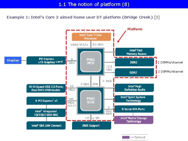
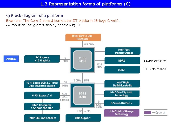
1. 1 The notion of platform (8) Example 1: Intel’s Core 2 aimed home user DT platform (Bridge Creek) [3] Platform 1066 MT/s Display card 2 DIMMs/channel C-link

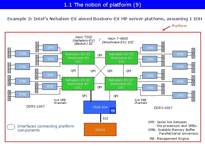
1. 1 The notion of platform (9) Example 2: Intel’s Nehalem-EX aimed Boxboro-EX MP server platform, assuming 1 IOH Platform Xeon 7500 (Nehalem-EX) (Becton) 8 C / Xeon 7 -4800 (Westmere-EX) 10 C SMB SMB Nehalem-EX 8 C Westmere-EX 10 C QPI SMB SMB QPI QPI SMB SMB Nehalem-EX 8 C Westmere-EX 10 C QPI DDR 3 -1067 SMB QPI 2 x 4 SMI channels 7500 IOH ESI Interfaces connecting platform components SMB ICH 10 ME DDR 3 -1067 SMI: Serial link between the processors and SMBs SMB: Scalable Memory Buffer Parallel/serial conversion ME: Management Engine

1. 1 The notion of platform (9) The structure of a platform is termed as its architecture (or topology). It describes the basic components and their interconnections and will be discussed in Section 3.

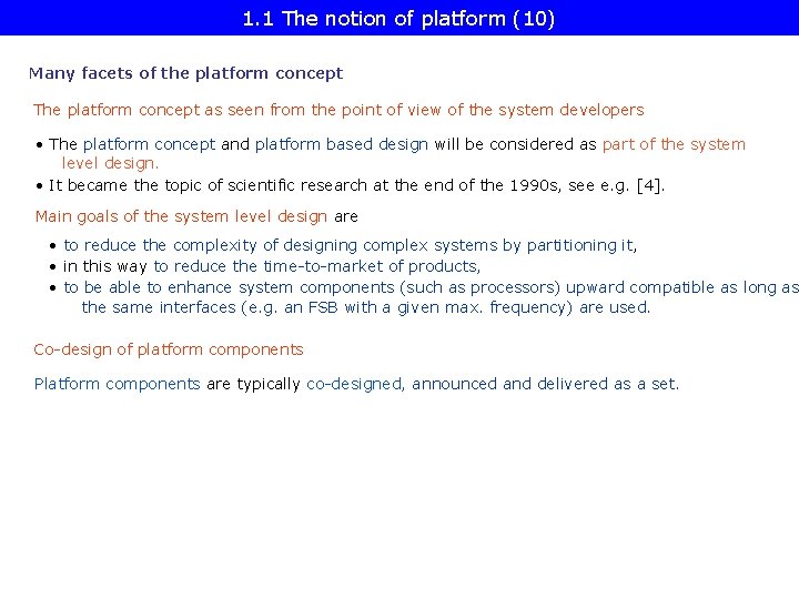
1. 1 The notion of platform (10) Many facets of the platform concept The platform concept as seen from the point of view of the system developers • The platform concept and platform based design will be considered as part of the system level design. • It became the topic of scientific research at the end of the 1990 s, see e. g. [4]. Main goals of the system level design are • to reduce the complexity of designing complex systems by partitioning it, • in this way to reduce the time-to-market of products, • to be able to enhance system components (such as processors) upward compatible as long as the same interfaces (e. g. an FSB with a given max. frequency) are used. Co-design of platform components Platform components are typically co-designed, announced and delivered as a set.

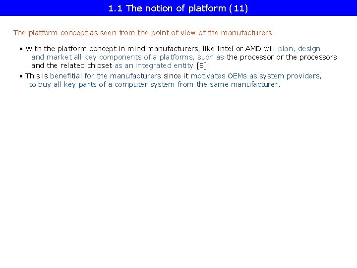
1. 1 The notion of platform (11) The platform concept as seen from the point of view of the manufacturers • With the platform concept in mind manufacturers, like Intel or AMD will plan, design and market all key components of a platforms, such as the processor or the processors and the related chipset as an integrated entity [5]. • This is benefitial for the manufacturers since it motivates OEMs as system providers, to buy all key parts of a computer system from the same manufacturer.

1. 1 The notion of platform (12) The platform concept as seen from the point of view of the customers The platform concept is benefitial for the customers as well since an integrated “backbone” of a system architecture promises a more reliable and more cost effective system.

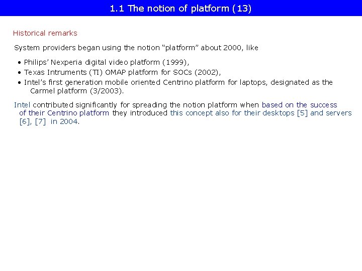
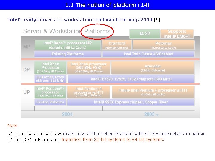
1. 1 The notion of platform (13) Historical remarks System providers began using the notion “platform” about 2000, like • Philips’ Nexperia digital video platform (1999), • Texas Intruments (TI) OMAP platform for SOCs (2002), • Intel’s first generation mobile oriented Centrino platform for laptops, designated as the Carmel platform (3/2003). Intel contributed significantly for spreading the notion platform when based on the success of their Centrino platform they introduced this concept also for their desktops [5] and servers [6], [7] in 2004.

1. 1 The notion of platform (14) Intel’s early server and workstation roadmap from Aug. 2004 [6] Note a) This roadmap already makes use of the notion platform without revealing platform names. b) In 2004 Intel made a transition from 32 bit systems to 64 bit systems.

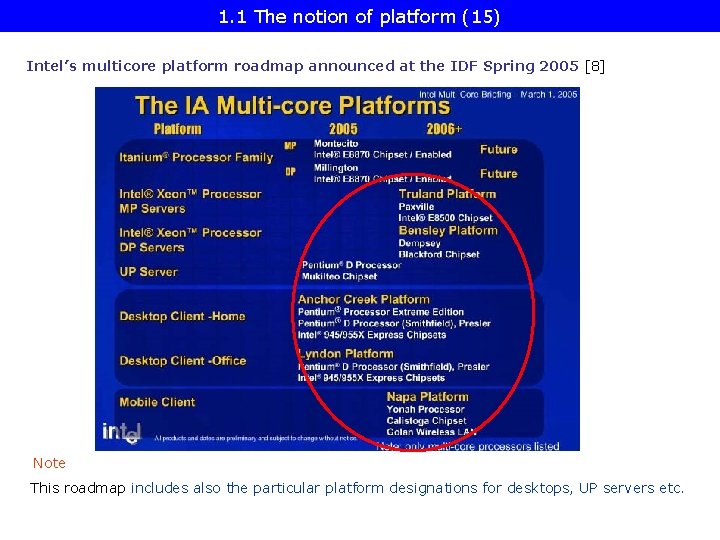
1. 1 The notion of platform (15) Intel’s multicore platform roadmap announced at the IDF Spring 2005 [8] Note This roadmap includes also the particular platform designations for desktops, UP servers etc.

1. 2. Description of a particular platform

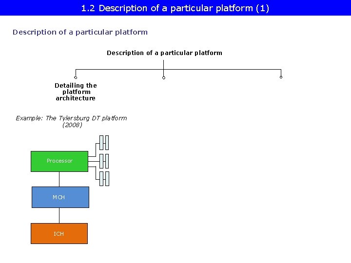
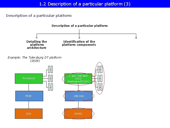
1. 2 Description of a particular platform (1) Description of a particular platform Detailing the platform architecture Example: The Tylersburg DT platform (2008) Processor MCH ICH

1. 2 Description of a particular platform (2) Detailing the platform architecture includes the architecture of the processor-, the memoryand the i/O subsystems (to be discussed in Section 3). It is concerned with issues, such as whether the processors of an MP server are connected to the MCH via an FSB or otherwise, or whether the memory is attached to the system architecture through the MCH or through the processors etc. ).

1. 2 Description of a particular platform (3) Description of a particular platform Detailing the platform architecture Identification of the platform components Example: The Tylersburg DT platform (2008) Processor 1. gen. Nehalem (4 C)/ Westmere-EP (6 C) MCH X 58 IOH ICH 10

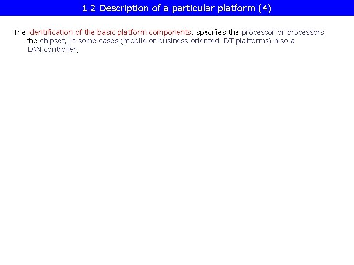
1. 2 Description of a particular platform (4) The identification of the basic platform components, specifies the processor or processors, the chipset, in some cases (mobile or business oriented DT platforms) also a LAN controller,

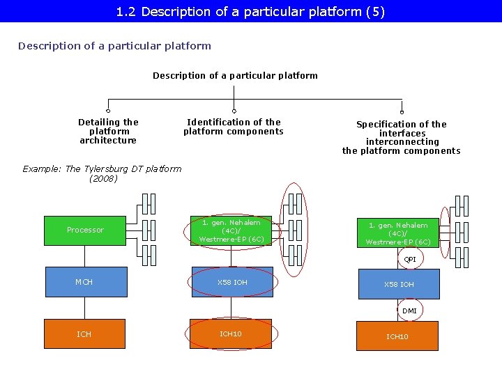
1. 2 Description of a particular platform (5) Description of a particular platform Detailing the platform architecture Identification of the platform components Specification of the interfaces interconnecting the platform components Example: The Tylersburg DT platform (2008) Processor 1. gen. Nehalem (4 C)/ Westmere-EP (6 C) QPI MCH X 58 IOH DMI ICH 10

1. 2 Description of a particular platform (6) The specification of the interfaces describes the buses (links) that interconnect platform components.

1. 2 Description of a particular platform (7) Remark The specification of a platform will be completed by the datasheets of the related platform components.

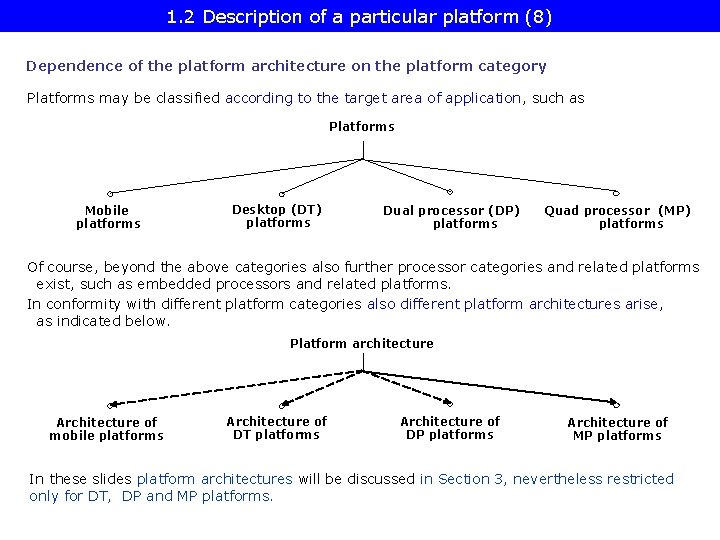
1. 2 Description of a particular platform (8) Dependence of the platform architecture on the platform category Platforms may be classified according to the target area of application, such as Platforms Mobile platforms Desktop (DT) platforms Dual processor (DP) platforms Quad processor (MP) platforms Of course, beyond the above categories also further processor categories and related platforms exist, such as embedded processors and related platforms. In conformity with different platform categories also different platform architectures arise, as indicated below. Platform architecture Architecture of mobile platforms Architecture of DT platforms Architecture of DP platforms Architecture of MP platforms In these slides platform architectures will be discussed in Section 3, nevertheless restricted only for DT, DP and MP platforms.

1. 3. Representation forms of platforms

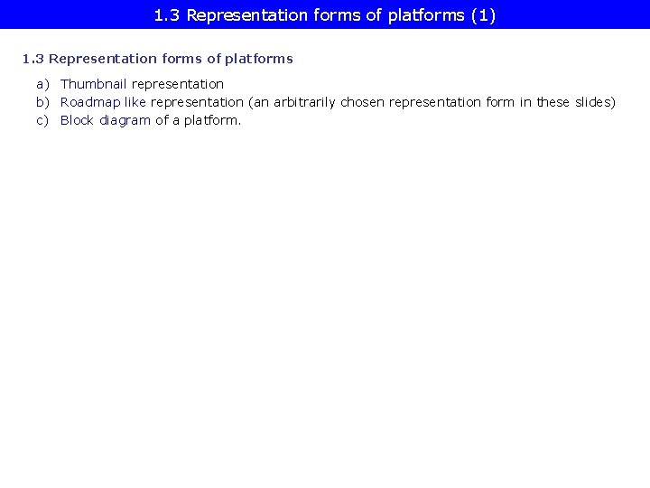
1. 3 Representation forms of platforms (1) 1. 3 Representation forms of platforms a) Thumbnail representation b) Roadmap like representation (an arbitrarily chosen representation form in these slides) c) Block diagram of a platform.

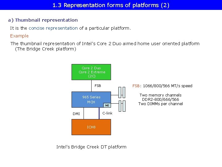
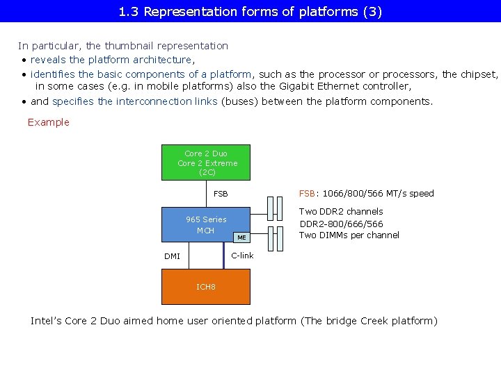
1. 3 Representation forms of platforms (2) a) Thumbnail representation It is the concise representation of a particular platform. Example The thumbnail representation of Intel’s Core 2 Duo aimed home user oriented platform (The Bridge Creek platform) Core 2 Duo Core 2 Extreme (2 C) FSB 965 Series MCH FSB: 1066/800/566 MT/s speed ME C-link DMI ICH 8 Intel’s Bridge Creek DT platform Two memory channels DDR 2 -800/666/566 Two DIMMs per channel

1. 3 Representation forms of platforms (3) In particular, the thumbnail representation • reveals the platform architecture, • identifies the basic components of a platform, such as the processor or processors, the chipset, in some cases (e. g. in mobile platforms) also the Gigabit Ethernet controller, • and specifies the interconnection links (buses) between the platform components. Example Core 2 Duo Core 2 Extreme (2 C) FSB: 1066/800/566 MT/s speed FSB 965 Series MCH ME Two DDR 2 channels DDR 2 -800/666/566 Two DIMMs per channel C-link DMI ICH 8 Intel’s Core 2 Duo aimed home user oriented platform (The bridge Creek platform)

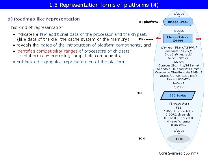
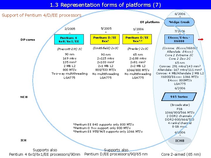
1. 3 Representation forms of platforms (4) 6/2006 b) Roadmap like representation DT platform This kind of representation • indicates a few additional data of the processor and the chipset, DP cores (like data of the die, the cache system or the memory) • reveals the dates of the introduction of platform components, and • identifies compatibility ranges of processors or chipsets in platforms by encircling compatible components, • but lacks the graphical representation of the platform. MCH Bridge Creek 7/2006 E 6 xxx/E 4 xxx X 6800 (Conroe: E 6 xxx/X 6800)1 Allendale: E 4 xxx)1 Core 2 Extreme 2 C Core 2 Duo 2 C 65 nm Conroe: 291 mtrs/143 mm 2 Allendale: 167 mtrs/111 mm 2 Conroe: 4 MB/Allendale 2 MB L 2 X 6800/E 6 xxx: 1066 MT/s E 4 xxx: 800 MT/s LGA 775 6/2006 965 Series (Broadwater) FSB 1066/800/566 MT/s 2 DDR 2 channels DDR 2 -800/666/533 4 ranks/channel 8 GB max. 6/2006 ICH 8 Core 2 -aimed (65 nm)

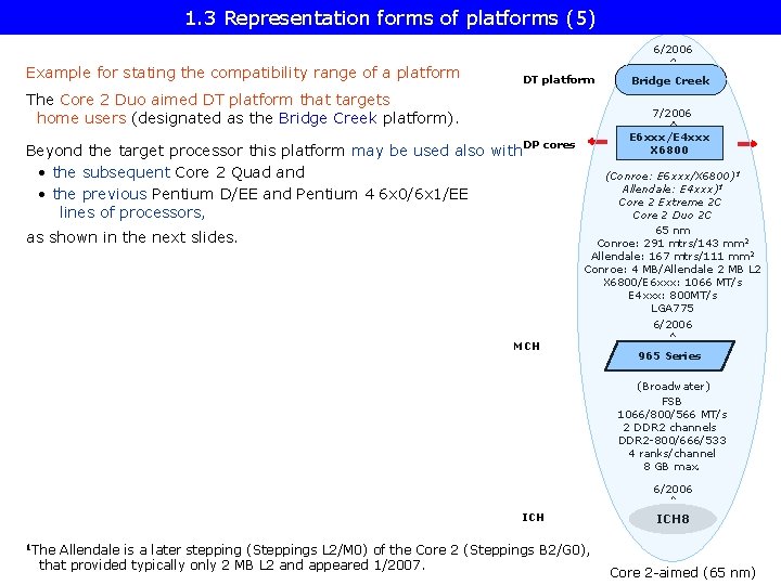
1. 3 Representation forms of platforms (5) 6/2006 Example for stating the compatibility range of a platform DT platform The Core 2 Duo aimed DT platform that targets home users (designated as the Bridge Creek platform). Bridge Creek 7/2006 Beyond the target processor this platform may be used also with. DP cores • the subsequent Core 2 Quad and • the previous Pentium D/EE and Pentium 4 6 x 0/6 x 1/EE lines of processors, as shown in the next slides. E 6 xxx/E 4 xxx X 6800 (Conroe: E 6 xxx/X 6800)1 Allendale: E 4 xxx)1 Core 2 Extreme 2 C Core 2 Duo 2 C 65 nm Conroe: 291 mtrs/143 mm 2 Allendale: 167 mtrs/111 mm 2 Conroe: 4 MB/Allendale 2 MB L 2 X 6800/E 6 xxx: 1066 MT/s E 4 xxx: 800 MT/s LGA 775 6/2006 MCH 965 Series (Broadwater) FSB 1066/800/566 MT/s 2 DDR 2 channels DDR 2 -800/666/533 4 ranks/channel 8 GB max. 6/2006 ICH Allendale is a later stepping (Steppings L 2/M 0) of the Core 2 (Steppings B 2/G 0), that provided typically only 2 MB L 2 and appeared 1/2007. ICH 8 1 The Core 2 -aimed (65 nm)

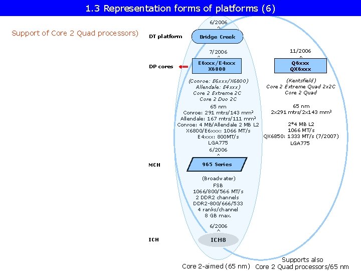
1. 3 Representation forms of platforms (6) 6/2006 Support of Core 2 Quad processors) DT platform DP cores Bridge Creek 7/2006 11/2006 E 6 xxx/E 4 xxx X 6800 Q 6 xxx QX 6 xxx (Kentsfield) (Conroe: E 6 xxx/X 6800) Core 2 Extreme Quad 2 x 2 C Allendale: E 4 xxx) Core 2 Quad Core 2 Extreme 2 C Core 2 Duo 2 C 65 nm 2 x 291 mtrs/2 x 143 mm 2 Conroe: 291 mtrs/143 mm 2 Allendale: 167 mtrs/111 mm 2 2*4 MB L 2 Conroe: 4 MB/Allendale 2 MB L 2 1066 MT/s X 6800/E 6 xxx: 1066 MT/s QX 6850: 1333 MT/s (7/2007) E 4 xxx: 800 MT/s LGA 775 6/2006 MCH 965 Series (Broadwater) FSB 1066/800/566 MT/s 2 DDR 2 channels DDR 2 -800/666/533 4 ranks/channel 8 GB max. 6/2006 ICH 8 Supports also Core 2 -aimed (65 nm) Core 2 Quad processors/65 nm

1. 3 Representation forms of platforms (7) 6/2006 Support of Pentium 4/D/EE processors DT platform 5/2005 2/2005 DP cores Pentium D/EE 8 xx 1 Pentium 4 6 x 0/6 x 1/EE 1/2006 Pentium D/EE 9 xx 2, 3 (Prescott-2 M) 1 C (Smithfield) 2 x 1 C (Presler) 2 x 1 C 90 nm 169 mtrs 135 mm 2 2 MB L 2 800 MT/s Two-way multithreading LGA 775 90 nm 2 x 115 mtrs 2 x 103 mm 2 2 x 1 MB L 2 800/533 MT/s No multithreading LGA 775 65 nm 2 x 188 mtrs 2 x 81 mm 2 2 x 2 MB L 2 1066/800 MT/s No multithreading LGA 775 Bridge Creek 7/2006 E 6 xxx/E 4 xxx X 6800 (Conroe: E 6 xxx/X 6800) Allendale: E 4 xxx) Core 2 Extreme 2 C Core 2 Duo 2 C 65 nm Conroe: 291 mtrs/143 mm 2 Allendale: 167 mtrs/111 mm 2 Conroe: 4 MB/Allendale 2 MB L 2 X 6800/E 6 xxx: 1066 MT/s E 4 xxx: 800 MT/s LGA 775 6/2006 965 Series MCH 1 Pentium EE 840 supports only 800 MT/s D 9 xx support only 800 MT/s 3 Pentium EE 955/965 supports only 1066 MT/s 2 Pentium ICH Supports also Pentium 4 6 x 0/6 x 1/EE processors/90 nm (Broadwater) FSB 1066/800/566 MT/s 2 DDR 2 channels DDR 2 -800/666/533 4 ranks/channel 8 GB max. 6/2006 ICH 8 Supports also Pentium D/EE processors/90/65 nm Core 2 -aimed (65 nm)

1. 3 Representation forms of platforms (8) c) Block diagram of a platform Example: The Core 2 aimed home user DT platform (Bridge Creek) (without an integrated display controller) [3] 1066 MT/s Display card 2 DIMMs/channel C-link

1. 4. Compatibility of platform components

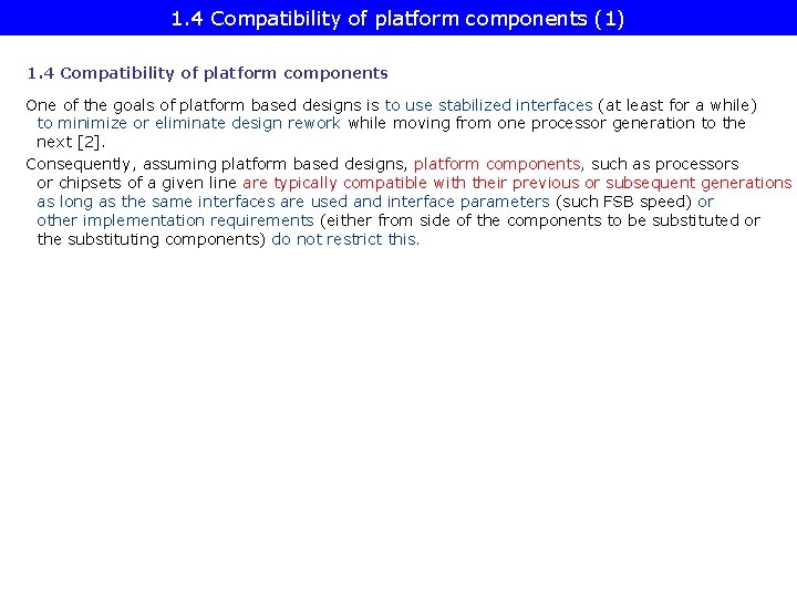
1. 4 Compatibility of platform components (1) 1. 4 Compatibility of platform components One of the goals of platform based designs is to use stabilized interfaces (at least for a while) to minimize or eliminate design rework while moving from one processor generation to the next [2]. Consequently, assuming platform based designs, platform components, such as processors or chipsets of a given line are typically compatible with their previous or subsequent generations as long as the same interfaces are used and interface parameters (such FSB speed) or other implementation requirements (either from side of the components to be substituted or the substituting components) do not restrict this.

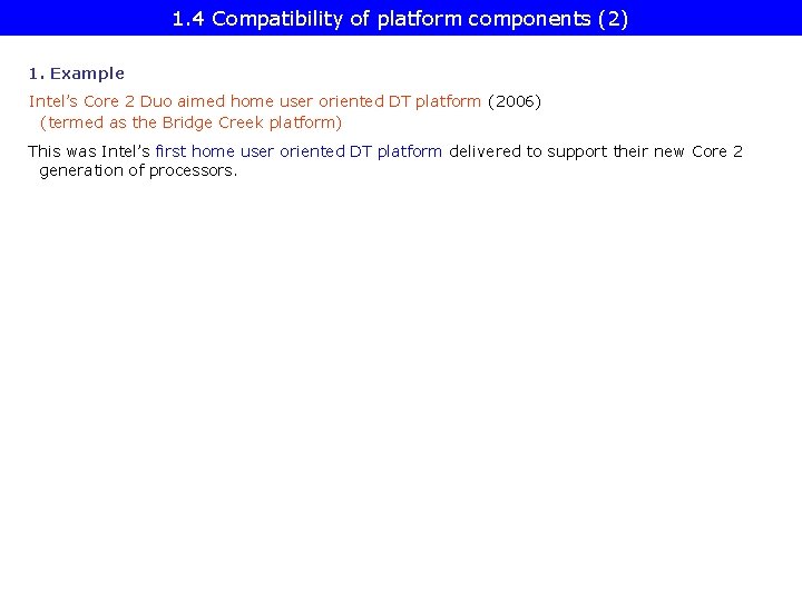
1. 4 Compatibility of platform components (2) 1. Example Intel’s Core 2 Duo aimed home user oriented DT platform (2006) (termed as the Bridge Creek platform) This was Intel’s first home user oriented DT platform delivered to support their new Core 2 generation of processors.

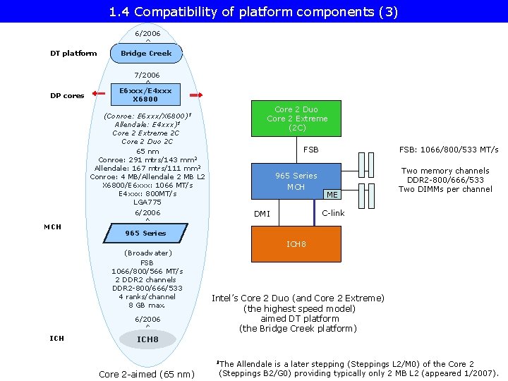
1. 4 Compatibility of platform components (3) 6/2006 DT platform Bridge Creek 7/2006 DP cores E 6 xxx/E 4 xxx X 6800 Core 2 Duo Core 2 Extreme (2 C) (Conroe: E 6 xxx/X 6800)1 Allendale: E 4 xxx)1 Core 2 Extreme 2 C Core 2 Duo 2 C 65 nm Conroe: 291 mtrs/143 mm 2 Allendale: 167 mtrs/111 mm 2 Conroe: 4 MB/Allendale 2 MB L 2 X 6800/E 6 xxx: 1066 MT/s E 4 xxx: 800 MT/s LGA 775 6/2006 MCH 965 Series MCH FSB: 1066/800/533 MT/s ME Two memory channels DDR 2 -800/666/533 Two DIMMs per channel C-link DMI 965 Series (Broadwater) FSB 1066/800/566 MT/s 2 DDR 2 channels DDR 2 -800/666/533 4 ranks/channel 8 GB max. 6/2006 ICH FSB ICH 8 Intel’s Core 2 Duo (and Core 2 Extreme) (the highest speed model) aimed DT platform (the Bridge Creek platform) ICH 8 1 The Core 2 -aimed (65 nm) Allendale is a later stepping (Steppings L 2/M 0) of the Core 2 (Steppings B 2/G 0) providing typically only 2 MB L 2 (appeared 1/2007).

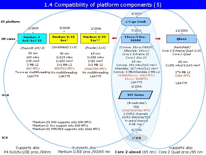
1. 4 Compatibility of platform components (4) In this DT platform the target processor is the Core 2, that is connected to the MCH by an FSB with 1066/800/533 MT/s. The target processor of the platform however, can be substituted • either by processors of three previous generations or • processors of the subsequent generation since all these processors have FSBs of 533/800/1066 MT/s, as shown in the next slide.

1. 4 Compatibility of platform components (5) 6/2006 DT platform Bridge Creek 2/2005 DP cores Pentium 4 6 x 0/6 x 1/EE (Prescott-2 M) 1 C 5/2005 Pentium D/EE 8 xx 1 (Smithfield) 2 x 1 C 90 nm 169 mtrs 2 x 115 mtrs 135 mm 2 2 x 103 mm 2 2 MB L 2 2 x 1 MB L 2 800 MT/s 800/533 MT/s Two-way multithreading No multithreading LGA 775 1/2006 Pentium D/EE 9 xx 2, 3 (Presler) 2 x 1 C 65 nm 2 x 188 mtrs 2 x 81 mm 2 2 x 2 MB L 2 1066/800 MT/s No multithreading LGA 775 7/2006 11/2006 E 6 xxx/E 4 xxx X 6800 Q 6 xxx (Conroe: E 6 xxx/X 6800) (Kentsfield) Allendale: E 4 xxx) Core 2 Extreme Quad 2 x 2 C Core 2 Extreme 2 C Core 2 Quad Core 2 Duo 2 C 65 nm Conroe: 291 mtrs/143 mm 2 2 x 291 mtrs/2 x 143 mm 2 Allendale: 167 mtrs/111 mm 2 Conroe: 4 MB/Allendale 2 MB L 2 2*4 MB L 2 X 6800/E 6 xxx: 1066 MT/s E 4 xxx: 800 MT/s LGA 775 6/2006 965 Series MCH 1 Pentium EE 840 supports only 800 MT/s D 9 xx support only 800 MT/s 3 Pentium EE 955/965 supports only 1066 MT/s 2 Pentium ICH Supports also P 4 6 x 0/6 x 1/EE proc. /90 nm (Broadwater) FSB 1066/800/566 MT/s 2 DDR 2 channels DDR 2 -800/666/533 4 ranks/channel 8 GB max. 6/2006 ICH 8 Supports also Pentium D/EE proc. /90/65 nm Supports also Core 2 -aimed (65 nm) Core 2 Quad proc. /65 nm

1. 4 Compatibility of platform components (6) Nevertheless, processors following the Core 2 Quad (including the highest performance level Core 2 Quad processor designated as the Core 2 Extreme Quad) provide already an increased FSB speed of 1333 MT/s and therefore are not more supported by the Core 2 aimed platform considered.

2. Main components of platforms • 2. 1. Processors • 2. 2. Buses interconnecting platform components • 2. 3. The memory subsystem

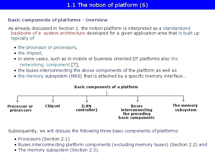
1. 1 The notion of platform (6) Basic components of platforms - Overview As already discussed in Section 1. the notion platform is interpreted as a standardized backbone of a system architecture developed for a given application area that is built up typically of • the processor or processors, • the chipset, • in some cases, such as in mobile or business oriented DT platforms also the networking component [7], • the buses interconnecting the above components of the platform as well as • the memory subsystem (MSS) that is attached by a specific memory interface. . Basic components of a platform Processor or processors Chipset (LAN controller) Buses interconnecting the preceding basic components The memory subsystem Subsequently, we will discuss the following three basic components of platforms: • Processors (Section 2. 1) • Buses interconnecting platform components (excluding memory buses) (Section 2. 2) and • The memory subsystem (Section 2. 3).

2. 1. Processors

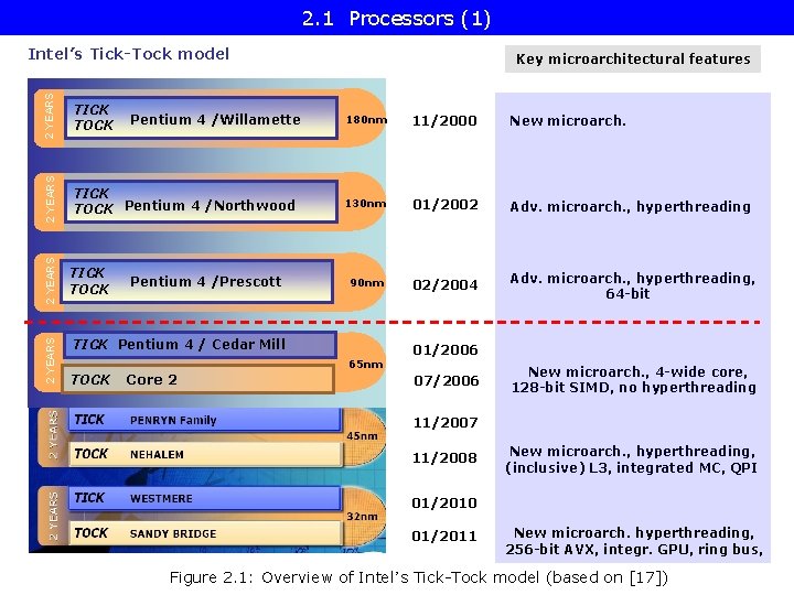
2. 1 Processors (1) 2 YEARS TICK TOCK Pentium 4 /Northwood 2 YEARS TICK TOCK 2 YEARS Intel’s Tick-Tock model TICK TOCK Pentium 4 /Willamette Pentium 4 /Prescott Key microarchitectural features 180 nm 11/2000 New microarch. 130 nm 01/2002 Adv. microarch. , hyperthreading 90 nm 02/2004 Adv. microarch. , hyperthreading, 64 -bit TICK Pentium 4 / Cedar Mill TOCK Core 2 65 nm 01/2006 07/2006 New microarch. , 4 -wide core, 128 -bit SIMD, no hyperthreading 11/2007 11/2008 New microarch. , hyperthreading, (inclusive) L 3, integrated MC, QPI 01/2010 01/2011 New microarch. hyperthreading, 256 -bit AVX, integr. GPU, ring bus, Figure 2. 1: Overview of Intel’s Tick-Tock model (based on [17])

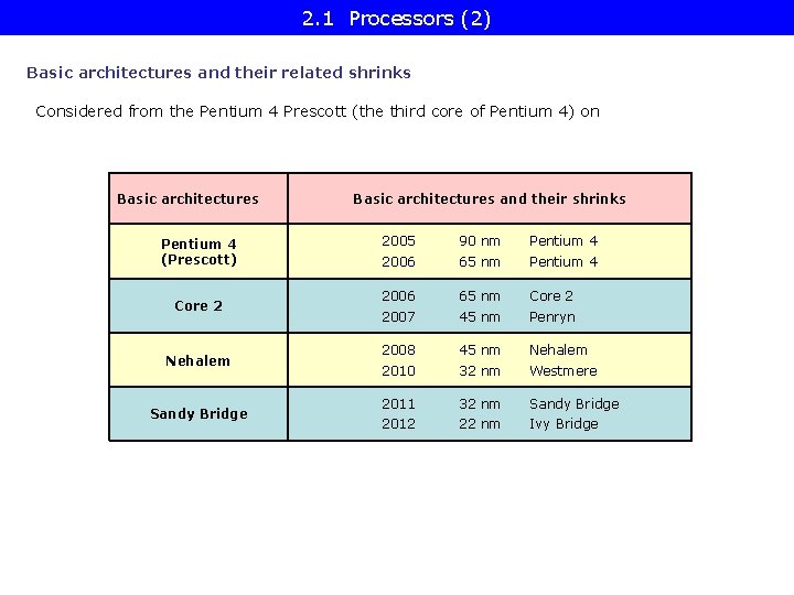
2. 1 Processors (2) Basic architectures and their related shrinks Considered from the Pentium 4 Prescott (the third core of Pentium 4) on Basic architectures Pentium 4 (Prescott) Core 2 Nehalem Sandy Bridge Basic architectures and their shrinks 2005 90 nm Pentium 4 2006 65 nm Core 2 2007 45 nm Penryn 2008 45 nm Nehalem 2010 32 nm Westmere 2011 32 nm Sandy Bridge 2012 22 nm Ivy Bridge

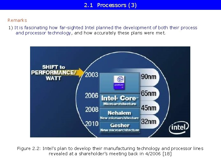
2. 1 Processors (3) Remarks 1) It is fascinating how far-sighted Intel planned the development of both their process and processor technology, and how accurately these plans were met. Figure 2. 2: Intel’s plan to develop their manufacturing technology and processor lines revealed at a shareholder’s meeting back in 4/2006 [18]

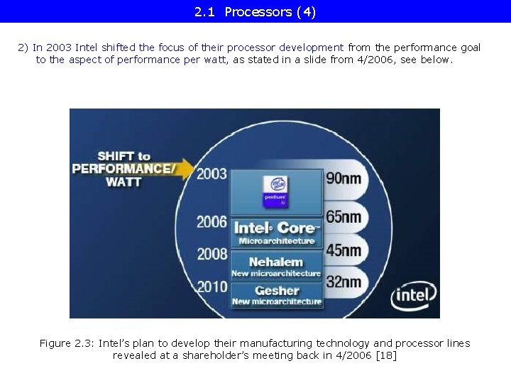
2. 1 Processors (4) 2) In 2003 Intel shifted the focus of their processor development from the performance goal to the aspect of performance per watt, as stated in a slide from 4/2006, see below. Figure 2. 3: Intel’s plan to develop their manufacturing technology and processor lines revealed at a shareholder’s meeting back in 4/2006 [18]

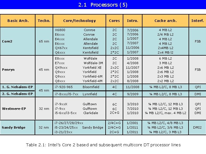
2. 1 Processors (5) Basic Arch. Core 2 Penryn 1. G. Nehalem-EP 2. G. Nehalem-EP Westmere-EP Sandy Bridge Techn. Core/technology Cores Intro. Cache arch. Interf. 65 nm X 6800 E 6 xxx E 4 xxx E 6 xxx QX 67 xx Q 6 xxx Conroe Allendale Kentsfield 2 C 2 C 2 x 2 C 2*2 C 7/2006 1/2007 7/2007 11/2006 1/2007 4 MB L 2 2/4 MB L 2 2 x 4 MB l 2 FSB 45 nm E 8 xxx E 7 xxx QX 9 xxx Q 8 xxx Wolfdale-3 M Yorkfield XE Yorkfield-6 M Yorkfield-4 M 2 C 2 C 2 x 2 C 2*2 C 2 x 2 C 1/2008 4/2008 11/2007 1/2008 8/2008 6 MB L 2 3 MB L 2 2 x 6 MB L 2 2 x 3 MB L 2 2 x 2 MB L 2 FSB i 7 -920 -965 Bloomfield 4 C 11/2008 ¼ MB L 2/C, 8 MB L 3 QPI i 7 -8 xxx/i 5 -7 xx Lynnfield 4 C 9/2009 ¼ MB L 2/C, 8 MB L 3 DMI 32 nm i 7 -9 xx. X i 7 -9 xx i 5 -6 xx/i 3 -5 xx Gulftown Clarkdale 6 C 6 C 2 C+G 3/2010 7/2010 1/2010 ¼ MB L 2/C, 12 MB L 3 ¼ MB L 2/C, max. 4 MB L 2 QPI DMI 32 nm i 7 -26/27/28/29 xx i 5 -23/24/25 xx Sandy Bridge i 3 -21/23 xx 2/4 C+G 2 C+G 1/2001 1/2011 ¼ MB L 2/C, 4/8 MB L 3 ¼ MB L 2/C, 3/6 MB L 3 ¼ MB L 2/C, 3 MB L 3 DMI 2 45 nm Table 2. 1: Intel’s Core 2 based and subsequent multicore DT processor lines

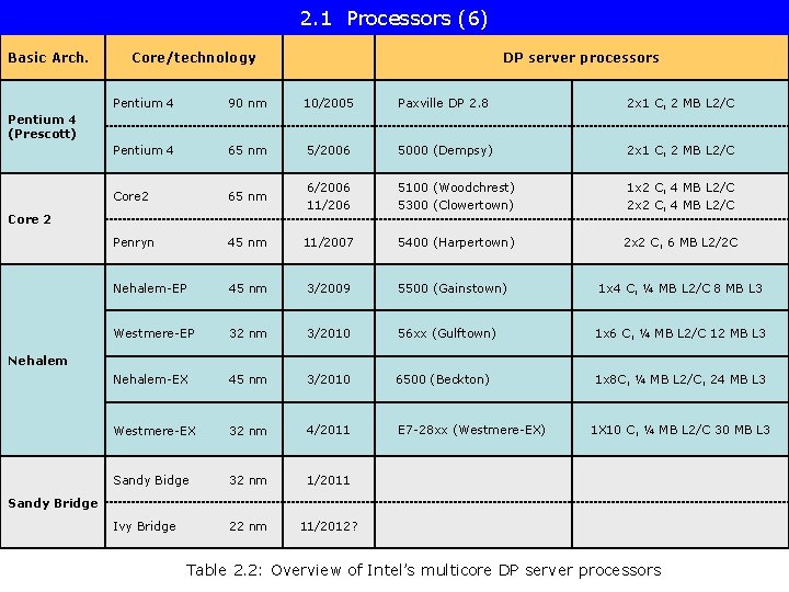
2. 1 Processors (6) Basic Arch. Core/technology DP server processors Pentium 4 90 nm 10/2005 Paxville DP 2. 8 2 x 1 C, 2 MB L 2/C Pentium 4 65 nm 5/2006 5000 (Dempsy) 2 x 1 C, 2 MB L 2/C Core 2 65 nm 6/2006 11/206 5100 (Woodchrest) 5300 (Clowertown) 1 x 2 C, 4 MB L 2/C 2 x 2 C, 4 MB L 2/C Penryn 45 nm 11/2007 5400 (Harpertown) 2 x 2 C, 6 MB L 2/2 C Nehalem-EP 45 nm 3/2009 5500 (Gainstown) Westmere-EP 32 nm 3/2010 56 xx (Gulftown) 1 x 6 C, ¼ MB L 2/C 12 MB L 3 Nehalem-EX 45 nm 3/2010 6500 (Beckton) 1 x 8 C, ¼ MB L 2/C, 24 MB L 3 Westmere-EX 32 nm 4/2011 E 7 -28 xx (Westmere-EX) Sandy Bidge 32 nm 1/2011 Ivy Bridge 22 nm 11/2012? Pentium 4 (Prescott) Core 2 1 x 4 C, ¼ MB L 2/C 8 MB L 3 Nehalem 1 X 10 C, ¼ MB L 2/C 30 MB L 3 Sandy Bridge Table 2. 2: Overview of Intel’s multicore DP server processors

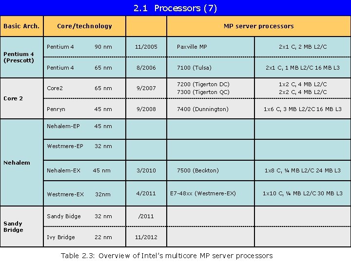
2. 1 Processors (7) Basic Arch. Core/technology MP server processors Pentium 4 90 nm 11/2005 Paxville MP 2 x 1 C, 2 MB L 2/C Pentium 4 65 nm 8/2006 7100 (Tulsa) Core 2 65 nm 9/2007 7200 (Tigerton DC) 7300 (Tigerton QC) 1 x 2 C, 4 MB L 2/C 2 x 2 C, 4 MB L 2/C Penryn 45 nm 9/2008 7400 (Dunnington) 1 x 6 C, 3 MB L 2/2 C 16 MB L 3 Nehalem-EP 45 nm Westmere-EP 32 nm Nehalem-EX 45 nm 3/2010 7500 (Beckton) 1 x 8 C, ¼ MB L 2/C 24 MB L 3 Westmere-EX 32 nm 4/2011 Sandy Bidge 32 nm /2011 Ivy Bridge 22 nm 11/2012 Pentium 4 (Prescott) Core 2 2 x 1 C, 1 MB L 2/C 16 MB L 3 Nehalem E 7 -48 xx (Westmere-EX) 1 x 10 C, ¼ MB L 2/C 30 MB L 3 Sandy Bridge Table 2. 3: Overview of Intel’s multicore MP server processors

2. 2. Buses interconnecting platform components

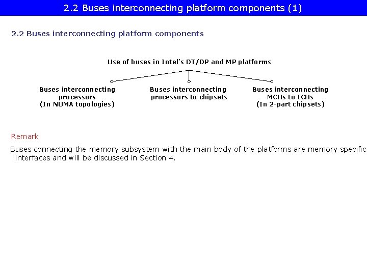
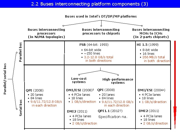
2. 2 Buses interconnecting platform components (1) 2. 2 Buses interconnecting platform components Use of buses in Intel’s DT/DP and MP platforms Buses interconnecting processors (In NUMA topologies) Buses interconnecting processors to chipsets Buses interconnecting MCHs to ICHs (In 2 -part chipsets) Remark Buses connecting the memory subsystem with the main body of the platforms are memory specific interfaces and will be discussed in Section 4.

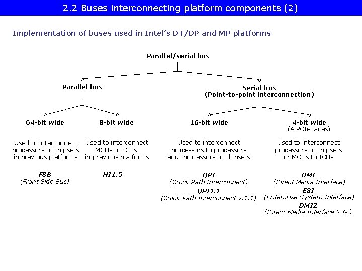
2. 2 Buses interconnecting platform components (2) Implementation of buses used in Intel’s DT/DP and MP platforms Parallel/serial bus Parallel bus 64 -bit wide Serial bus (Point-to-point interconnection) 8 -bit wide Used to interconnect MCHs to ICHs processors to chipsets in previous platforms FSB (Front Side Bus) HI 1. 5 16 -bit wide 4 -bit wide (4 PCIe lanes) Used to interconnect processors to processors and processors to chipsets Used to interconnect processors to chipsets or MCHs to ICHs QPI (Quick Path Interconnect) QPI 1. 1 (Quick Path Interconnect v. 1. 1) DMI (Direct Media Interface) ESI (Enterprise System Interface) DMI 2 (Direct Media Interface 2. G. )

2. 2 Buses interconnecting platform components (3) Buses used in Intel’s DT/DP/MP platforms Parallel/serial bus Parallel bus Buses interconnecting processors (In NUMA topologies) Buses interconnecting processors to chipsets FSB (64 -bit: 1993) • 64 -bit wide • ~150 lines • 3. 2 -12. 8 GB/s total in both directions Low-cost systems Serial bus Buses interconnecting MCHs to ICHs (In 2 -parts chipsets) QPI (2008) • 20 lanes • 84 lines • 9. 6/11. 72/12. 8 GB/s in each direction • 8 -bit wide • 16 lines • 266 MB/s total in both directions High-performance systems DMI/ESI (2008)2 QPI (2008) • 4 PCIe lanes • 20 lanes • 18 lines • 84 lines • 1 GB/s/direction • 9. 6/11. 72/12. 8 GB/s in each direction DMI 2 (2011) HI 1. 5 (1999) QPI 1. 1 (2012? ) • 4 PCIe lanes Specification na. • 18 lines • 2 GB/s/direction DMI/ESI (20041) • 4 PCIe lanes • 18 lines • 1 GB/s/direction DMI 2 (2011) • 4 PCIe lanes • 18 lines • 2 GB/s/direction

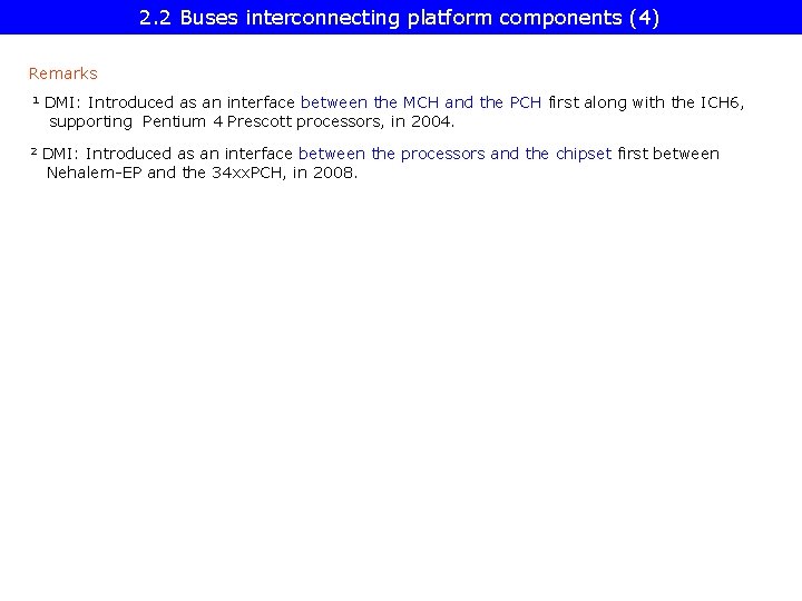
2. 2 Buses interconnecting platform components (4) Remarks 1 DMI: Introduced as an interface between the MCH and the PCH first along with the ICH 6, supporting Pentium 4 Prescott processors, in 2004. 2 DMI: Introduced as an interface between the processors and the chipset first between Nehalem-EP and the 34 xx. PCH, in 2008.

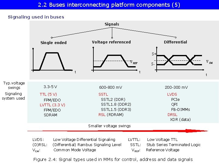
2. 2 Buses interconnecting platform components (5) Signaling used in buses Signals Voltage referenced Single ended Differential S+ VREF t t Typ. voltage swings 3. 3 -5 V Signaling system used TTL (5 V) FPM/EDO LVTTL (3. 3 V) FPM/EDO SDRAM VCM S- t 200 -300 m. V 600 -800 m. V SSTL 2 (DDR) SSTL 1. 8 (DDR 2) SSTL 1. 5 (DDR 3) RSL (RDRAM) LVDS PCIe QPI FB-DIMMs DRSL XDR (data) Smaller voltage swings LVDS: (D)RSL: VCM: Low Voltage Differential Signaling (Differential) Rambus Signaling Level Common Mode Voltage LVTTL: SSTL: V REF: Low Voltage TTL Stub Series Terminated Logic Reference Voltage Figure 2. 4: Signal types used in MMs for control, address and data signals

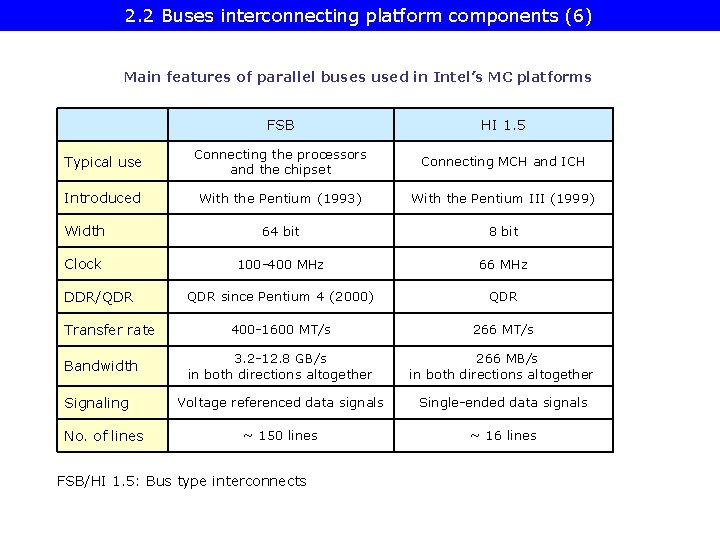
2. 2 Buses interconnecting platform components (6) Main features of parallel buses used in Intel’s MC platforms FSB HI 1. 5 Typical use Connecting the processors and the chipset Connecting MCH and ICH Introduced With the Pentium (1993) With the Pentium III (1999) Width 64 bit 8 bit Clock 100 -400 MHz 66 MHz QDR since Pentium 4 (2000) QDR 400 -1600 MT/s 266 MT/s 3. 2 -12. 8 GB/s in both directions altogether 266 MB/s in both directions altogether Voltage referenced data signals Single-ended data signals ~ 150 lines ~ 16 lines DDR/QDR Transfer rate Bandwidth Signaling No. of lines FSB/HI 1. 5: Bus type interconnects

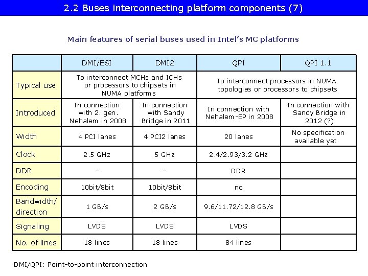
2. 2 Buses interconnecting platform components (7) Main features of serial buses used in Intel’s MC platforms DMI/ESI Typical use DMI 2 To interconnect MCHs and ICHs or processors to chipsets in NUMA platforms QPI 1. 1 To interconnect processors in NUMA topologies or processors to chipsets In connection with 2. gen. Nehalem in 2008 In connection with Sandy Bridge in 2011 In connection with Nehalem-EP in 2008 In connection with Sandy Bridge in 2012 (? ) Width 4 PCI lanes 4 PCI 2 lanes 20 lanes No specification available yet Clock 2. 5 GHz 2. 4/2. 93/3. 2 GHz DDR – – DDR 10 bit/8 bit no 1 GB/s 2 GB/s 9. 6/11. 72/12. 8 GB/s LVDS 18 lines 84 lines Introduced Encoding Bandwidth/ direction Signaling No. of lines DMI/QPI: Point-to-point interconnection

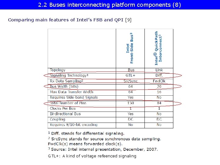
2. 2 Buses interconnecting platform components (8) Comparing main features of Intel’s FSB and QPI [9] GTL+: A kind of voltage refeenced signaling

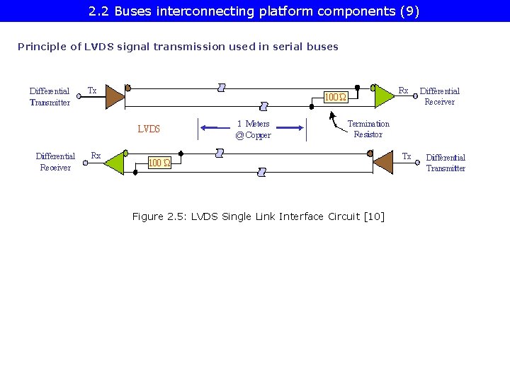
2. 2 Buses interconnecting platform components (9) Principle of LVDS signal transmission used in serial buses Figure 2. 5: LVDS Single Link Interface Circuit [10]

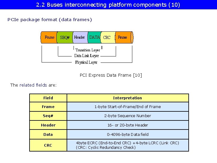
2. 2 Buses interconnecting platform components (10) PCIe package format (data frames) PCI Express Data Frame [10] The related fields are: Field Interpretation Frame 1 -byte Start-of-Frame/End of Frame Seq# 2 -byte Sequence Number Header 16 - or 20 -byte Header Data 0 -4096 -byte Data field CRC 4 byte ECRC (End-to-End CRC) +4 -byte LCRC (Link CRC) (CRC: Cyclic Redundancy Check)

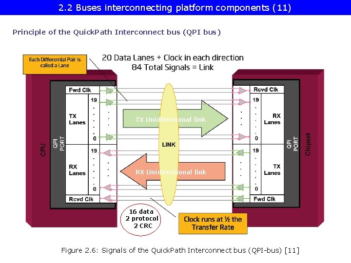
2. 2 Buses interconnecting platform components (11) Principle of the Quick. Path Interconnect bus (QPI bus) TX Unidirectional link RX Unidirectional link 16 data 2 protocol 2 CRC Figure 2. 6: Signals of the Quick. Path Interconnect bus (QPI-bus) [11]

2. 3. The memory subsystem • 2. 3. 1. Key parameters of the memory subsystem • 2. 3. 2. Main attributes of the memory technology used • 2. 3. 2. 1. Overview: Main attributes of the memory technology used • 2. 3. 2. 2. Memory type • 2. 3. Speed grades • 2. 3. 2. 4. DIMM density • 2. 3. 2. 5. Use of ECC support • 2. 3. 2. 6. Use of registering

2. 3. 1 Key performance parameters of the memory subsystem (1) 2. 3. 1 Key performance parameters of the memory subsystem This issue will be discussed in Section 4.

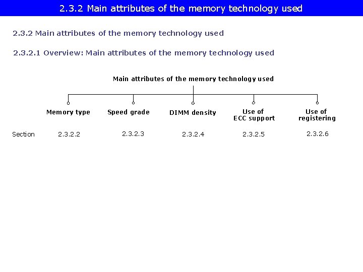
2. 3. 2 Main attributes of the memory technology used 2. 3. 2. 1 Overview: Main attributes of the memory technology used Memory type Section 2. 3. 2. 2 Speed grade 2. 3 DIMM density Use of ECC support Use of registering 2. 3. 2. 4 2. 3. 2. 5 2. 3. 2. 6

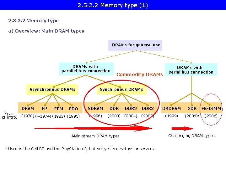
2. 3. 2. 2 Memory type (1) 2. 3. 2. 2 Memory type a) Overview: Main DRAM types DRAMs for general use DRAMs with parallel bus connection Asynchronous DRAM Year of intro. FP FPM EDO (1970) (~1974) (1983) (1995) Commodity DRAMs Synchronous DRAMs SDRAM (1996) DDR 2 DDR 3 DRDRAM XDR FB-DIMM (2000) (2004) (2007) (1999) (2006)1 (2006) DDR Main stream DRAM types 1 DRAMs with serial bus connection Used in the Cell BE and the Play. Station 3, but not yet in desktops or servers Challenging DRAM types

2. 3. 2. 2 Memory type (2) b) Synchronous DRAMs (SDRAM, DDR 2, DDR 3)

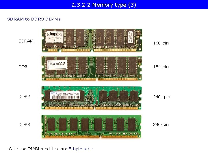
2. 3. 2. 2 Memory type (3) SDRAM to DDR 3 DIMMs SDRAM 168 -pin DDR 184 -pin DDR 2 240 - pin DDR 3 240 -pin All these DIMM modules are 8 -byte wide

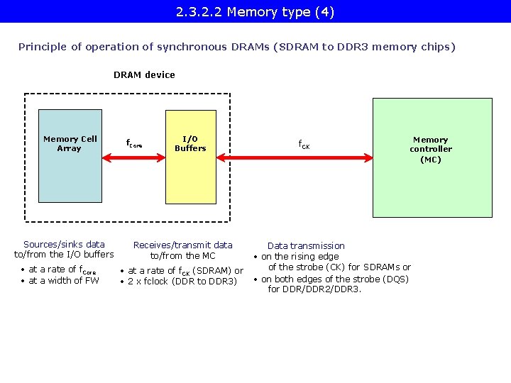
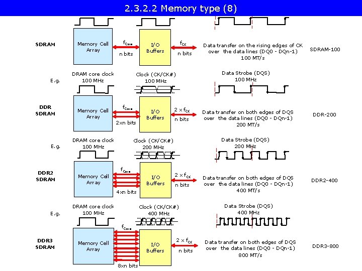
2. 3. 2. 2 Memory type (4) Principle of operation of synchronous DRAMs (SDRAM to DDR 3 memory chips) DRAM device Memory Cell Array Sources/sinks data to/from the I/O buffers • at a rate of f. Core • at a width of FW f. Core I/O Buffers Receives/transmit data to/from the MC • at a rate of f. CK (SDRAM) or • 2 x fclock (DDR to DDR 3) f. CK Memory controller (MC) Data transmission • on the rising edge of the strobe (CK) for SDRAMs or • on both edges of the strobe (DQS) for DDR/DDR 2/DDR 3.

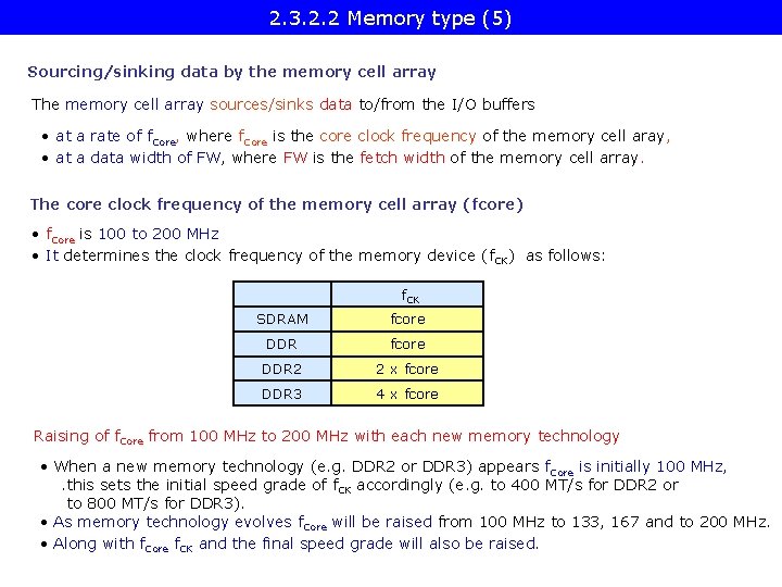
2. 3. 2. 2 Memory type (5) Sourcing/sinking data by the memory cell array The memory cell array sources/sinks data to/from the I/O buffers • at a rate of f. Core, where f. Core is the core clock frequency of the memory cell aray, • at a data width of FW, where FW is the fetch width of the memory cell array. The core clock frequency of the memory cell array (fcore) • f. Core is 100 to 200 MHz • It determines the clock frequency of the memory device (f. CK) as follows: f. CK SDRAM fcore DDR 2 2 x fcore DDR 3 4 x fcore Raising of f. Core from 100 MHz to 200 MHz with each new memory technology • When a new memory technology (e. g. DDR 2 or DDR 3) appears f. Core is initially 100 MHz, . this sets the initial speed grade of f. CK accordingly (e. g. to 400 MT/s for DDR 2 or to 800 MT/s for DDR 3). • As memory technology evolves f. Core will be raised from 100 MHz to 133, 167 and to 200 MHz. • Along with f. Core f. CK and the final speed grade will also be raised.

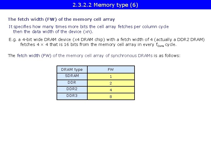
2. 3. 2. 2 Memory type (6) The fetch width (FW) of the memory cell array It specifies how many times more bits the cell array fetches per column cycle then the data width of the device (xn). E. g. a 4 -bit wide DRAM device (x 4 DRAM chip) with a fetch width of 4 (actually a DDR 2 DRAM) fetches 4 × 4 that is 16 bits from the memory cell array in every f. Core cycle. The fetch width (FW) of the memory cell array of synchronous DRAMs is as follows: DRAM type FW SDRAM 1 DDR 2 4 DDR 3 8

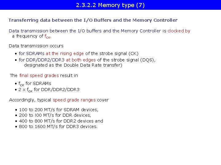
2. 3. 2. 2 Memory type (7) Transferring data between the I/O Buffers and the Memory Controller Data transmission between the I/O buffers and the Memory Controller is clocked by a frequency of f. CK. Data transmission occurs • for SDRAMs at the rising edge of the strobe signal (CK) • for DDR/DDR 2/DDR 3 at both edges of the strobe signal (DQS), designated as the Double Data Rate transfer) The final speed grades result in • f. CK for SDRAMs • 2 x f. CK for DDR/DDR 2/DDR 3 Accordingly, typical speed grade ranges cover • • 100 200 400 800 to to 200 MT/s for SDRAM devices, !00 MT/s for DDR devices, 800 MT/s for DDR 2 devices and 1600 MT/s for DDR 3 devices.

E. g. SDRAM E. g. DDR 2 SDRAM core frequency 100 MHz Memory Cell Array Clock frequency (f ) (CK) 2. 3. 2. 2 Memory type (8) Clock 100 MHz CK f. Core n bits DRAM core clock 100 MHz Memory Cell Array n bits f. Core 2 xn bits I/O Buffers 2 x f. CK n bits 4 xn bits E. g. DRAM core clock 100 MHz SDRAM-100 Data transfer on both edges of DQS over the data lines (DQ 0 - DQn-1) 200 MT/s DDR-200 Data Strobe (DQS) 200 MHz Clock (CK/CK#) 200 MHz f. Core Data transfer on the rising edges of CK over the data lines (DQ 0 - DQn-1) 100 MT/s Data Strobe (DQS) 100 MHz Clock (CK/CK#) 100 MHz DRAM core clock 100 MHz Memory Cell Array f. CK I/O Buffers Clock (CK/CK#) 400 MHz Data transfer on both edges of DQS over the data lines (DQ 0 - DQn-1) 400 MT/s DDR 2 -400 Data Strobe (DQS) 400 MHz f. Core DDR 3 SDRAM Memory Cell Array I/O Buffers 8 xn bits 2 x f. CK n bits Data transfer on both edges of DQS over the data lines (DQ 0 - DQn-1) 800 MT/s DDR 3 -800

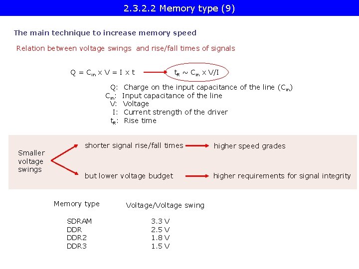
2. 3. 2. 2 Memory type (9) The main technique to increase memory speed Relation between voltage swings and rise/fall times of signals Q = Cin x V = I x t Q: Cin: V: I: t. R: Smaller voltage swings t. R ~ Cin x V/I Charge on the input capacitance of the line (Cin) Input capacitance of the line Voltage Current strength of the driver Rise time shorter signal rise/fall times higher speed grades but lower voltage budget higher requirements for signal integrity Memory type SDRAM DDR 2 DDR 3 Voltage/Voltage swing 3. 3 2. 5 1. 8 1. 5 V V

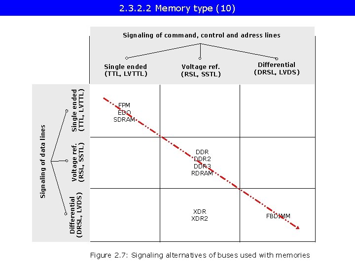
2. 3. 2. 2 Memory type (10) Signaling of command, control and adress lines Single ended (TTL, LVTTL) Voltage ref. (RSL, SSTL) Differential (DRSL, LVDS) Signaling of data lines Single ended (TTL, LVTTL) Voltage ref. (RSL, SSTL) Differential (DRSL, LVDS) FPM EDO SDRAM DDR 2 DDR 3 RDRAM XDR 2 FBDIMM Figure 2. 7: Signaling alternatives of buses used with memories

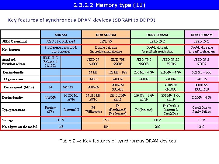
2. 3. 2. 2 Memory type (11) Key features of synchronous DRAM devices (SDRAM to DDR 3) JEDEC standard Key features SDRAM DDR 2 SDRAM DDR 3 SDRAM JESD 21 -C Release 4 JESD 79 -2 JESD 79 -3 Synchronous, pipelined, burst oriented Double data rate 2 n prefetch architecture Double data rate 4 n prefetch architecture Double data rate 8 n pref. architecture JESD 21 -C Release 4 11/1993 JESD 79 6/2000 JESD 79 E 5/2005 JESD 79 -2 9/2003 JESD 79 -2 C 5/2006 JESD 79 -3 6/2007 Device density 64 Mb 128 Mb - 1 Gb 256 Mb - 4 Gb 256 Mb – 4 Gb 512 Mb – 8 Gb Organization x 4/8/16 x 4/8/16 200/266/ 333/400 400/533/ 667/800 800/1066/ 1333/1600 16 -256 Mb x 8/16 64 -512 Mb x 8/16 128 -512 Mb x 8/16 256 Mb – 1 Gb x 8/16 256 Mb -1 Gb x 8/16 512 Mb – 4 Gb Pentium III P 4 (Willamette) P 4 (Northwood) P 4 (Prescott) P 4 (Presler) Pentium D Core 2 Duo to Sandy Bridge Standard First/last release Device speed (MT/s) 66 Device density 4/16 Mb Typ. processors Pentium (3 V) Voltage No. of pins on the modul 100/133 3. 3 V 2. 5 V 1. 8 V 1. 5 V 168 184 240 Table 2. 4: Key features of synchronous DRAM devices

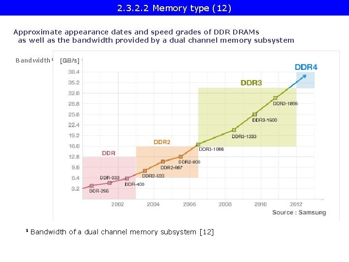
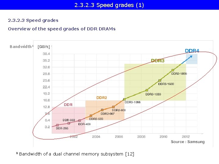
2. 3. 2. 2 Memory type (12) Approximate appearance dates and speed grades of DDR DRAMs as well as the bandwidth provided by a dual channel memory subsystem Bandwidth 1 1 Bandwidth of a dual channel memory subsystem [12]

2. 3. 2. 2 Memory type (13) Green and ultra-low power memories They represents the latest achievements of the DRAM memory technology Green memories: lower dissipation memories Ultra-low-power DDR 3 memories: Use of 1. 35 V supply voltage instead of 1. 50 V to reduce dissipation
![2 3 2 2 Memory type 14 Green and ultralow power memories Examples 13 2. 3. 2. 2 Memory type (14) Green and ultra-low power memories- Examples [13]](https://slidetodoc.com/presentation_image_h2/63bf6bfb565824c352f6768862af55ac/image-83.jpg)
2. 3. 2. 2 Memory type (14) Green and ultra-low power memories- Examples [13]

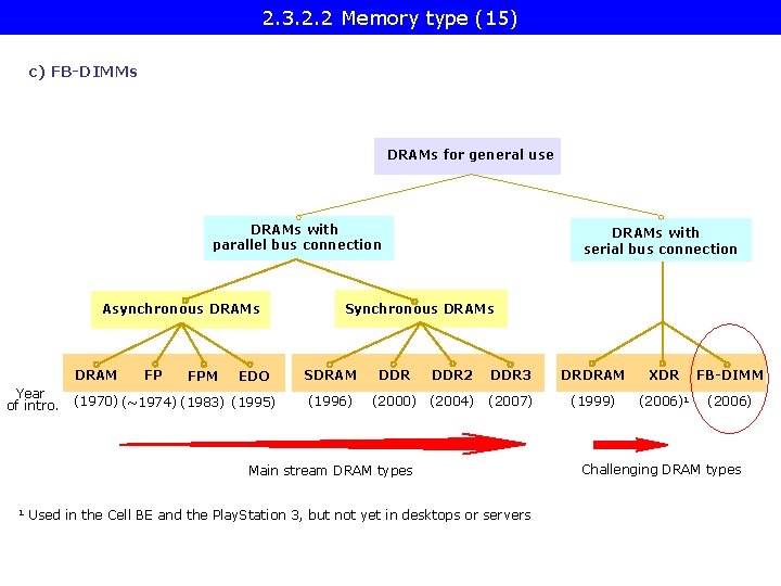
2. 3. 2. 2 Memory type (15) c) FB-DIMMs DRAMs for general use DRAMs with parallel bus connection Asynchronous DRAM Year of intro. FP FPM EDO (1970) (~1974) (1983) (1995) DRAMs with serial bus connection Synchronous DRAMs SDRAM (1996) DDR 2 DDR 3 DRDRAM XDR FB-DIMM (2000) (2004) (2007) (1999) (2006)1 (2006) DDR Main stream DRAM types 1 Used in the Cell BE and the Play. Station 3, but not yet in desktops or servers Challenging DRAM types

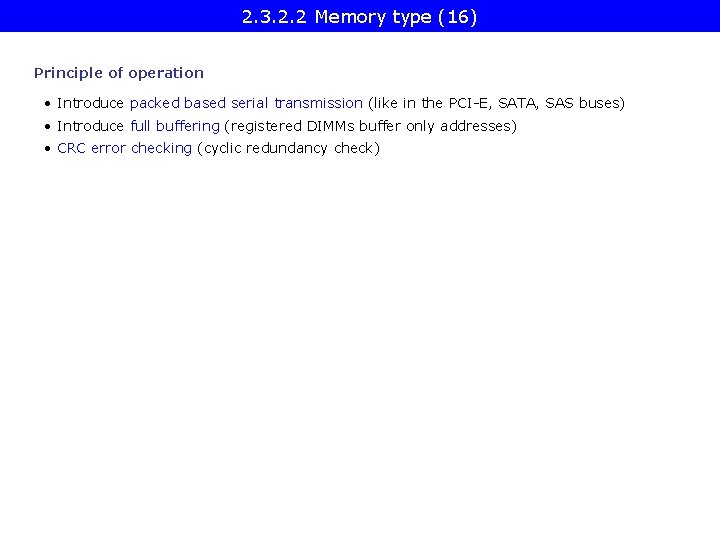
2. 3. 2. 2 Memory type (16) Principle of operation • Introduce packed based serial transmission (like in the PCI-E, SATA, SAS buses) • Introduce full buffering (registered DIMMs buffer only addresses) • CRC error checking (cyclic redundancy check)
![2 3 2 2 Memory type 17 The architecture of FBDIMM memories 19 2. 3. 2. 2 Memory type (17) The architecture of FB-DIMM memories [19]](https://slidetodoc.com/presentation_image_h2/63bf6bfb565824c352f6768862af55ac/image-86.jpg)
2. 3. 2. 2 Memory type (17) The architecture of FB-DIMM memories [19]

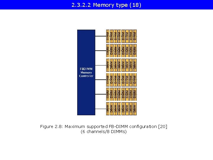
2. 3. 2. 2 Memory type (18) Figure 2. 8: Maximum supported FB-DIMM configuration [20] (6 channels/8 DIMMs)

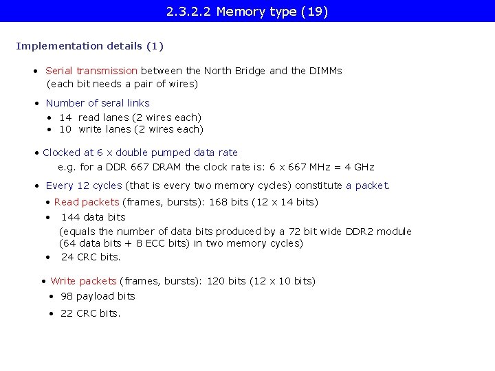
2. 3. 2. 2 Memory type (19) Implementation details (1) • Serial transmission between the North Bridge and the DIMMs (each bit needs a pair of wires) • Number of seral links • 14 read lanes (2 wires each) • 10 write lanes (2 wires each) • Clocked at 6 x double pumped data rate e. g. for a DDR 667 DRAM the clock rate is: 6 x 667 MHz = 4 GHz • Every 12 cycles (that is every two memory cycles) constitute a packet. • Read packets (frames, bursts): 168 bits (12 x 14 bits) • 144 data bits (equals the number of data bits produced by a 72 bit wide DDR 2 module (64 data bits + 8 ECC bits) in two memory cycles) • 24 CRC bits. • Write packets (frames, bursts): 120 bits (12 x 10 bits) • 98 payload bits • 22 CRC bits.

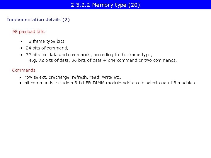
2. 3. 2. 2 Memory type (20) Implementation details (2) 98 payload bits. • 2 frame type bits, • 24 bits of command, • 72 bits for data and commands, according to the frame type, e. g. 72 bits of data, 36 bits of data + one command or two commands. Commands • row select, precharge, refresh, read, write etc. • all commands include a 3 -bit FB-DIMM module address to select one of 8 modules.

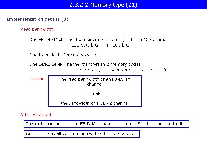
2. 3. 2. 2 Memory type (21) Implementation details (3) Read bandwidth: One FB-DIMM channel transfers in one frame (that is in 12 cycles): 128 data bits, + 16 ECC bits One frame lasts 2 memory cycles One DDR 2 DIMM channel transfers in 2 memory cycles: 2 x 72 bits (2 x 64 -bit data + 2 x 8 -bit ECC) The read bandwidth of an FB-DIMM channel equals the bandwidth of a DDR 2 channel Write bandwidth: The write bandwidth of an FB-DIMM channel is up to 0. 5 x the read bandwidth. But FB-DIMMs allow simultan read and write operation

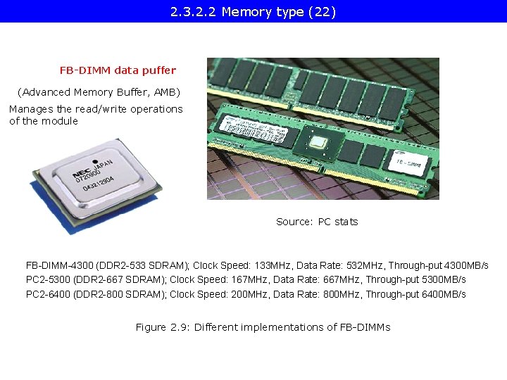
2. 3. 2. 2 Memory type (22) FB-DIMM data puffer (Advanced Memory Buffer, AMB) Manages the read/write operations of the module Source: PC stats FB-DIMM-4300 (DDR 2 -533 SDRAM); Clock Speed: 133 MHz, Data Rate: 532 MHz, Through-put 4300 MB/s PC 2 -5300 (DDR 2 -667 SDRAM); Clock Speed: 167 MHz, Data Rate: 667 MHz, Through-put 5300 MB/s PC 2 -6400 (DDR 2 -800 SDRAM); Clock Speed: 200 MHz, Data Rate: 800 MHz, Through-put 6400 MB/s Figure 2. 9: Different implementations of FB-DIMMs

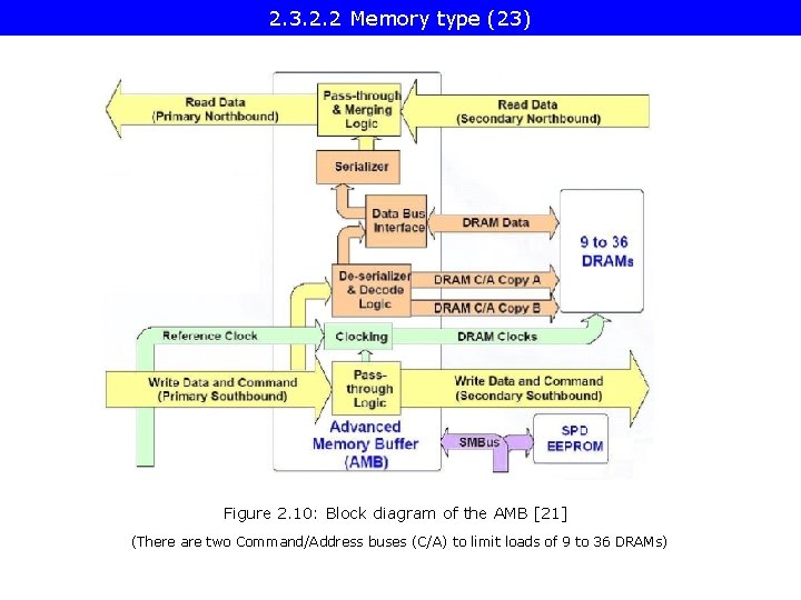
2. 3. 2. 2 Memory type (23) Figure 2. 10: Block diagram of the AMB [21] (There are two Command/Address buses (C/A) to limit loads of 9 to 36 DRAMs)

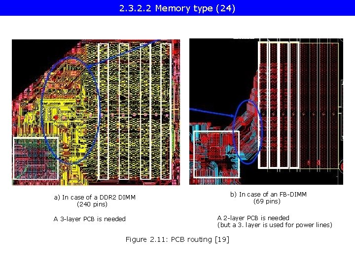
2. 3. 2. 2 type Necessary routing to connect the north bridge to. Memory the DIMM socket (24) b) In case of an FB-DIMM (69 pins) a) In case of a DDR 2 DIMM (240 pins) A 3 -layer PCB is needed A 2 -layer PCB is needed (but a 3. layer is used for power lines) Figure 2. 11: PCB routing [19]

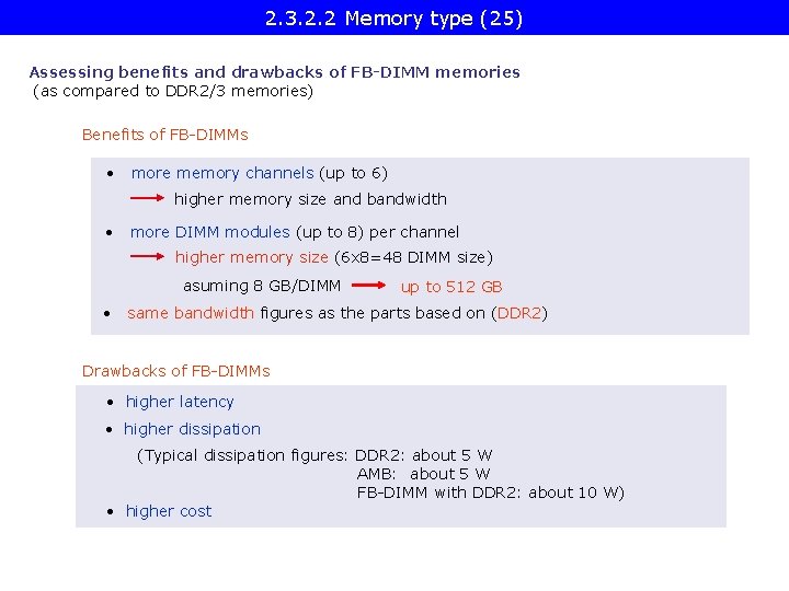
2. 3. 2. 2 Memory type (25) Assessing benefits and drawbacks of FB-DIMM memories (as compared to DDR 2/3 memories) Benefits of FB-DIMMs • more memory channels (up to 6) higher memory size and bandwidth • more DIMM modules (up to 8) per channel higher memory size (6 x 8=48 DIMM size) asuming 8 GB/DIMM • up to 512 GB same bandwidth figures as the parts based on (DDR 2) Drawbacks of FB-DIMMs • higher latency • higher dissipation (Typical dissipation figures: DDR 2: about 5 W AMB: about 5 W FB-DIMM with DDR 2: about 10 W) • higher cost
![2 3 2 2 Memory type 26 Latency 22 Due to their additional 2. 3. 2. 2 Memory type (26) Latency [22] • Due to their additional](https://slidetodoc.com/presentation_image_h2/63bf6bfb565824c352f6768862af55ac/image-95.jpg)
2. 3. 2. 2 Memory type (26) Latency [22] • Due to their additional serialization tasks and daisy-chained nature FB-DIMMs have about 15 % higher overall average latency than DDR 2 memories. • At low system utilization the additional serialization cost dominates, thus FB-DIMMs have higher latency figures than DDR 2 memories. • At higher system utilization, an FB-DIMM memory with a higher number of channels has the benefit to support a larger number of in-flight transactions, that results in a lower overall latency than a DDR 2 memory provides. Production The production of FB-DIMMs stopped with DDR 2 -800 modules, no DDR 3 modules came to the market due to the drawbacks of the technology.

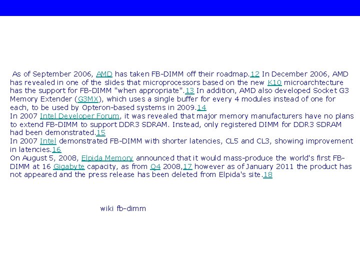
As of September 2006, AMD has taken FB-DIMM off their roadmap. 12 In December 2006, AMD has revealed in one of the slides that microprocessors based on the new K 10 microarchtecture has the support for FB-DIMM "when appropriate". 13 In addition, AMD also developed Socket G 3 Memory Extender (G 3 MX), which uses a single buffer for every 4 modules instead of one for each, to be used by Opteron-based systems in 2009. 14 In 2007 Intel Developer Forum, it was revealed that major memory manufacturers have no plans to extend FB-DIMM to support DDR 3 SDRAM. Instead, only registered DIMM for DDR 3 SDRAM had been demonstrated. 15 In 2007 Intel demonstrated FB-DIMM with shorter latencies, CL 5 and CL 3, showing improvement in latencies. 16 On August 5, 2008, Elpida Memory announced that it would mass-produce the world's first FBDIMM at 16 Gigabyte capacity, as from Q 4 2008, 17 however as of January 2011 the product has not appeared and the press release has been deleted from Elpida's site. 18 wiki fb-dimm

2. 3 Speed grades (1) 2. 3 Speed grades Overview of the speed grades of DDR DRAMs Bandwidth 1 1 Bandwidth of a dual channel memory subsystem [12]

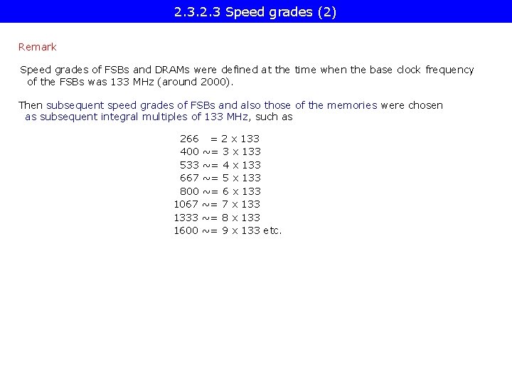
2. 3 Speed grades (2) Remark Speed grades of FSBs and DRAMs were defined at the time when the base clock frequency of the FSBs was 133 MHz (around 2000). Then subsequent speed grades of FSBs and also those of the memories were chosen as subsequent integral multiples of 133 MHz, such as 266 = 2 x 133 400 ~= 3 x 133 533 ~= 4 x 133 667 ~= 5 x 133 800 ~= 6 x 133 1067 ~= 7 x 1333 ~= 8 x 133 1600 ~= 9 x 133 etc.

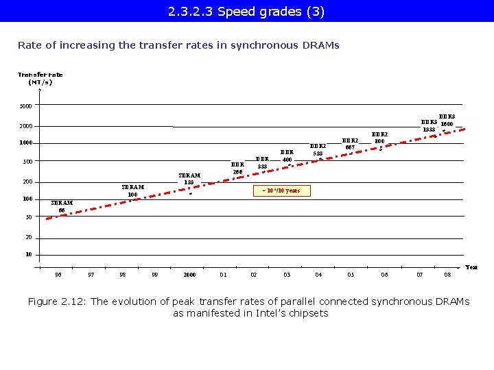
2. 3 Speed grades (3) Rate of increasing the transfer rates in synchronous DRAMs Transfer rate (MT/s) 5000 2000 1000 500 200 100 50 SDRAM 133 SDRAM 100 * SDRAM 66 * DDR 266 * DDR 333 * DDR 400 * DDR 2 533 * DDR 2 667 * DDR 2 800 * DDR 3 1600 1333 * * ~ 10*/10 years * 20 10 Year 96 97 98 99 2000 01 02 03 04 05 06 07 08 Figure 2. 12: The evolution of peak transfer rates of parallel connected synchronous DRAMs as manifested in Intel’s chipsets

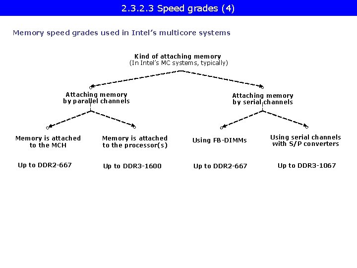
2. 3 Speed grades (4) Memory speed grades used in Intel’s multicore systems Kind of attaching memory (In Intel’s MC systems, typically) Attaching memory by parallel channels Memory is attached to the MCH Up to DDR 2 -667 Attaching memory by serial channels Memory is attached to the processor(s) Using FB-DIMMs Using serial channels with S/P converters Up to DDR 3 -1600 Up to DDR 2 -667 Up to DDR 3 -1067

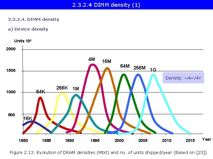
2. 3. 2. 4 DIMM density (1) 2. 3. 2. 4. DIMM density a) Device density Units 106 2000 4 M 1500 16 M 64 M 256 M 1 G Density: ~4×/4 Y 64 K 1000 500 256 K 1 M 16 K 1980 1985 1990 1995 2000 2005 2010 2015 Year Figure 2. 13: Evolution of DRAM densities (Mbit) and no. of units shipped/year (Based on [23])

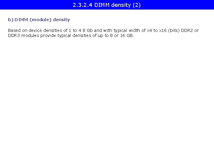
2. 3. 2. 4 DIMM density (2) b) DIMM (module) density Based on device densities of 1 to 4 8 Gb and with typical width of x 4 to x 16 (bits) DDR 2 or DDR 3 modules provide typical densities of up to 8 or 16 GB.

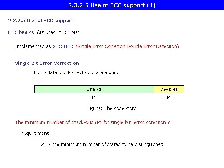
2. 3. 2. 5 Use of ECC support (1) 2. 3. 2. 5 Use of ECC support ECC basics (as used in DIMMs) Implemented as SEC-DED (Single Error Corretion Double Error Detection) Single bit Error Correction For D data bits P check-bits are added. Data bits Check bits D P Figure: The code word The minimum number of check-bits (P) for single bit error corection ? Requirement: 2 P ≥ the minimum number of states to be distinguished.

2. 3. 2. 5 Use of ECC support (2) The minimum number of states to be distinguished: • It is needed to specify the bit position of a possible single bit error in the code word consisting of both data and check bits This requires D + P states • one additional state to specify the „no error” state. the minimum number of states to be distinguished is: D + P + 1 Accordingly: to implement single bit error correction the minimum number of check bits (P) needs to satisfy the requirement: 2 P ≥ D + P + 1

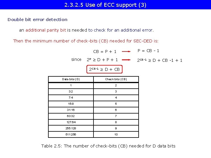
2. 3. 2. 5 Use of ECC support (3) Double bit error detection an additional parity bit is needed to check for an additional error. Then the minimum number of check-bits (CB) needed for SEC-DED is: CB = P + 1 since 2 P ≥ D + P + 1 P = CB - 1 2 CB-1 ≥ D + CB -1 + 1 2 CB-1 ≥ D + CB Data bits (D) Check bits (CB) 1 2 3: 2 3 7: 4 4 15: 8 5 31: 16 6 63: 32 7 127: 64 8 255: 128 9 511: 256 10 Table 2. 5: The number of check-bits (CB) needed for D data bits

2. 3. 2. 5 Use of ECC support (4) Supported memory features of DT and DP/MP platforms DT memories typically do not support ECC or registered (buffered) DIMMs, in contrast servers make typically use of registered DIMMs with ECC protection.

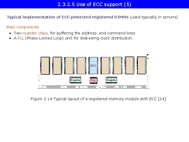
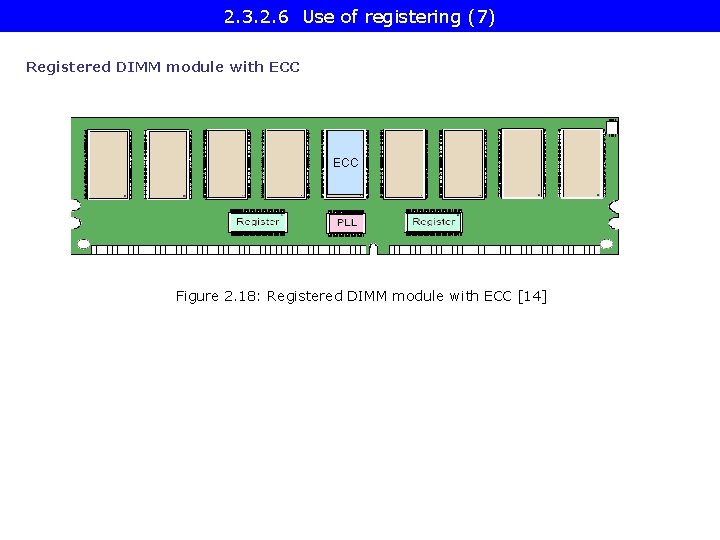
2. 3. 2. 5 Use of ECC support (5) Typical implementation of ECC protected registered DIMMs (used typically in servers) Main components • Two register chips, for buffering the address- and command lines • A PLL (Phase Locked Loop) unit for deskewing clock distribution. ECC Register PLL Register Figure 2. 14: Typical layout of a registered memory module with ECC [14]

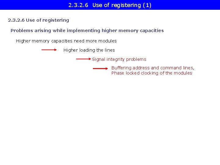
2. 3. 2. 6 Use of registering (1) 2. 3. 2. 6 Use of registering Problems arising while implementing higher memory capacities Higher memory capacities need more modules Higher loading the lines Signal integrity problems Buffering address and command lines, Phase locked clocking of the modules

2. 3. 2. 6 Use of registering (2) Registering Principle Buffering address and control lines • to reduce signal loading in a memory channel • in order to increase the number of supported DIMM slots (max. mem. capacity), needed first of all in servers,

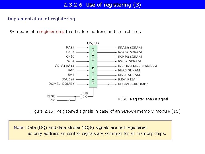
2. 3. 2. 6 Use of registering (3) Implementation of registering By means of a register chip that buffers address and control lines R E G I S T E R REGE: Register enable signal Figure 2. 15: Registered signals in case of an SDRAM memory module [15] Note: Data (DQ) and data strobe (DQS) signals are not registered as only address an control signals are common for all memory chips.

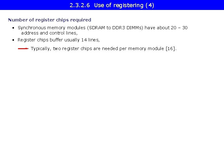
2. 3. 2. 6 Use of registering (4) Number of register chips required • Synchronous memory modules (SDRAM to DDR 3 DIMMs) have about 20 – 30 address and control lines, • Register chips buffer usually 14 lines, Typically, two register chips are needed per memory module [16].

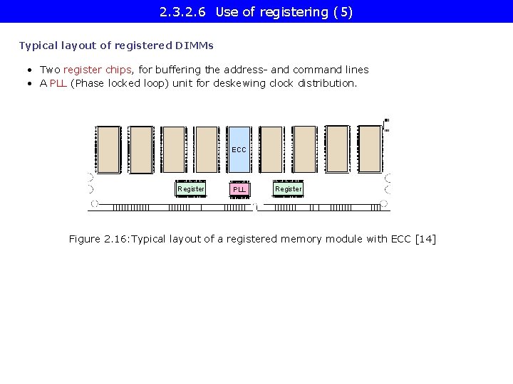
2. 3. 2. 6 Use of registering (5) Typical layout of registered DIMMs • Two register chips, for buffering the address- and command lines • A PLL (Phase locked loop) unit for deskewing clock distribution. ECC Register PLL Register Figure 2. 16: Typical layout of a registered memory module with ECC [14]

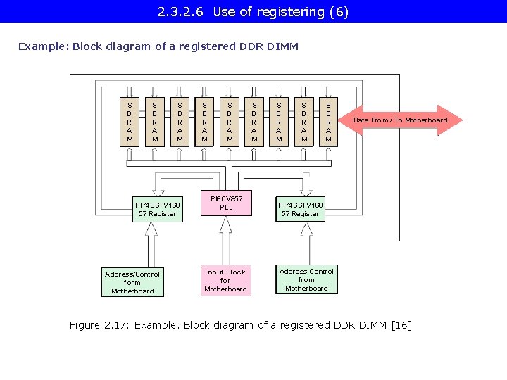
2. 3. 2. 6 Use of registering (6) Example: Block diagram of a registered DDR DIMM S D R A M PI 74 SSTV 168 57 Register Address/Control form Motherboard S D R A M PI 6 CV 857 PLL Input Clock for Motherboard S D R A M Data From / To Motherboard PI 74 SSTV 168 57 Register Address Control from Motherboard Figure 2. 17: Example. Block diagram of a registered DDR DIMM [16]

2. 3. 2. 6 Use of registering (7) Registered DIMM module with ECC Figure 2. 18: Registered DIMM module with ECC [14]

2. 3. 2. 6 Use of registering (8) Typical use of unregistered DIMMs (UDIMMs) in desktops/laptops (Memory capacities: up to a few GB) Typical use of registered DIMM (RDIMM) in servers (Memory capacities: a few tens of GB to a few hundreds of GB)

5. References
![5 References 1 1 Wikipedia Centrino http en wikipedia orgwikiCentrino 2 Industry Uniting Around 5. References (1) [1]: Wikipedia: Centrino, http: //en. wikipedia. org/wiki/Centrino [2]: Industry Uniting Around](https://slidetodoc.com/presentation_image_h2/63bf6bfb565824c352f6768862af55ac/image-117.jpg)
5. References (1) [1]: Wikipedia: Centrino, http: //en. wikipedia. org/wiki/Centrino [2]: Industry Uniting Around Intel Server Architecture; Platform Initiatives Complement Strong Intel IA-32 and IA-64 Targeted Processor Roadmap for 1999, Business Wire, Febr. 24 1999, http: //www. thefreelibrary. com/Industry+Uniting+Around+Intel+Server +Architecture%3 B+Platform. . . -a 053949226 [3]: Intel Core 2 Duo Processor, http: //www. intel. com/pressroom/kits/core 2 duo/ [4]: Keutzer K. , Malik S. , Newton R. , Rabaey J. , Sangiovanni-Vincentelli A. , System Level Design: Orthogonalization of Concerns and Platform-Based Design, IEEE Transactions on Computer-Aided Design of Circuits and Systems, Vol. 19, No. 12, Dec. 2000, pp. 1 -29. [5]: Krazit T. , Intel Sheds Light on 2005 Desktop Strategy, IDG News Service, Dec. 07 2004, http: //pcworld. about. net/news/Dec 072004 id 118866. htm [6]: Perich D. , Intel Volume platforms Technology Leadership, Presentation at HP World 2004, http: //98. 190. 245. 141: 8080/Proceed/HPW 04 CD/papers/4194. pdf [7] Powerful New Intel Server Platforms Feature Array Of Enterprise-Class Innovations. Intel’s Press release, Aug. 2, 2004 , http: //www. intel. com/pressroom/archive/releases/20040802 comp. htm [8]: Smith S. , Multi-Core Briefing, IDF Spring 2005, San Francisco, Press presentation, March 1 2005, http: //www. silentpcreview. com/article 224 -page 2 [9]: An Introduction to the Intel Quick. Path Interconnect, Jan. 2009, http: //www. intel. com/ content/dam/doc/white-paper/quick-path-interconnect-introduction-paper. pdf [10]: Davis L. PCI Express Bus, http: //www. interfacebus. com/PCI-Express-Bus-PCIe-Description. html
![5 References 2 11 Ng P K High End Desktop Platform Design Overview 5. References (2) [11]: Ng P. K. , “High End Desktop Platform Design Overview](https://slidetodoc.com/presentation_image_h2/63bf6bfb565824c352f6768862af55ac/image-118.jpg)
5. References (2) [11]: Ng P. K. , “High End Desktop Platform Design Overview for the Next Generation Intel Microarchitecture (Nehalem) Processor, ” IDF Taipei, TDPS 001, 2008, http: //intel. wingateweb. com/taiwan 08/published/sessions/TDPS 001/FA 08%20 IDFTaipei_TDPS 001_100. pdf [12]: Computing DRAM, Samsung. com, http: //www. samsung. com/global/business/semiconductor /products/dram/Products_Computing. DRAM. html [13]: Samsung’s Green DDR 3 – Solution 3, 20 nm class 1. 35 V, Sept. 2011, http: //www. samsung. com/global/business/semiconductor/Greenmemory/Downloads/ Documents/downloads/green_ddr 3_2011. pdf [14]: DDR SDRAM Registered DIMM Design Specification, JEDEC Standard No. 21 -C, Page 4. 20. 4 -1, Jan. 2002, http: //www. jedec. org [15]: Datasheet, http: //download. micron. com/pdf/datasheets/modules/sdram/ SD 9 C 16_32 x 72. pdf [16]: Solanki V. , „Design Guide Lines for Registered DDR DIMM Module, ” Application Note AN 37, Pericom, Nov. 2001, http: //www. pericom. com/pdf/applications/AN 037. pdf [17]: Fisher S. , “Technical Overview of the 45 nm Next Generation Intel Core Microarchitecture (Penryn), ” IDF 2007, ITPS 001, http: //isdlibrary. intel-dispatch. com/isd/89/45 nm. pdf [18]: Razin A. , Core, Nehalem, Gesher. Intel: New Architecture Every Two Years, Xbit Laboratories, 04/28/2006, http: //www. xbitlabs. com/news/cpu/display/20060428162855. html [19]: Haas, J. & Vogt P. , Fully buffered DIMM Technology Moves Enterprise Platforms to the Next Level, ” Technology Intel Magazine, March 2005, pp. 1 -7
![5 References 3 20 Introducing FBDIMM Memory Birth of Serial RAM PCStats 5. References (3) [20]: „Introducing FB-DIMM Memory: Birth of Serial RAM? , ” PCStats,](https://slidetodoc.com/presentation_image_h2/63bf6bfb565824c352f6768862af55ac/image-119.jpg)
5. References (3) [20]: „Introducing FB-DIMM Memory: Birth of Serial RAM? , ” PCStats, Dec. 23, 2005, http: //www. pcstats. com/articleview. cfm? articleid=1812&page=1 [21]: Mc. Tague M. & David H. , „ Fully Buffered DIMM (FB-DIMM) Design Considerations, ” Febr. 18, 2004, Intel Developer Forum, http: //www. idt. com/content/OSA-S 009. pdf [22]: Ganesh B. , Jaleel A. , Wang D. , Jacob B. , Fully-Buffered DIMM Memory Architectures: Understanding Mechanisms, Overheads and Scaling, 2007, [23]: DRAM Pricing – A White Paper, Tachyon Semiconductors, http: //www. tachyonsemi. com/about/papers/DRAM%Pricing. pdf