Microprocessors I Intel MCs 51 Introduction CS00871 Prof
- Slides: 56

Microprocessors I Intel MCs 51 Introduction CS-00871 Prof. Msc. Ivan A. Escobar iescobar@itesm. mx

Introduction l l PCs, microprocessor based systems, are much more visible. Embedded control with microcontrollers vastly outnumber u. P systems. – – Automotive Toys Appliances Consumer Electronics

History of Microcont vs Microp. l l l 1971 Intel introduced the 8080 – 1 st u. P. 1976 Intel introduced the 8748 – u. C. 1980 Intel introduced the 8051 - The first in the MCS 51 line. – – l 4 K Bytes ROM 128 Bytes RAM 32 I/O lines 2 16 -bit timers. The 8051 is well established and new variations of the 8051 continue to be developed.

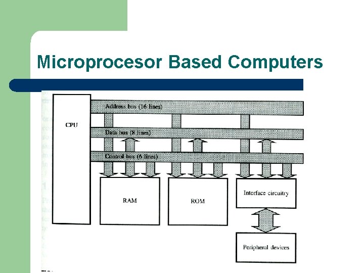
Microprocessor Based Computers l l l A CPU with external RAM, ROM, and devices. Address, data and control buses are used for data transfer. Microprocessors are fairly useless without being combined with numerous other components.

Microprocesor Based Computers

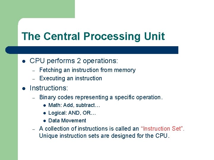
The Central Processing Unit l CPU performs 2 operations: – – l Fetching an instruction from memory Executing an instruction Instructions: – Binary codes representing a specific operation. l l l – Math: Add, subtract… Logical: AND, OR… Data Movement A collection of instructions is called an “Instruction Set”. Unique instruction sets are designed for the CPU.

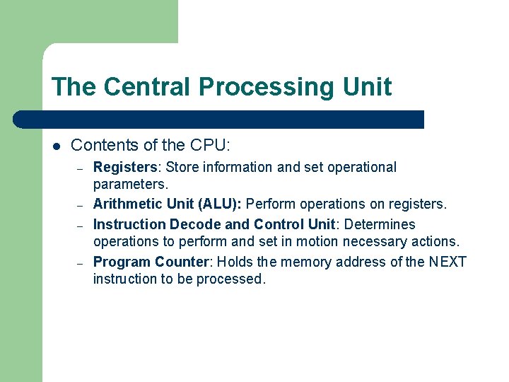
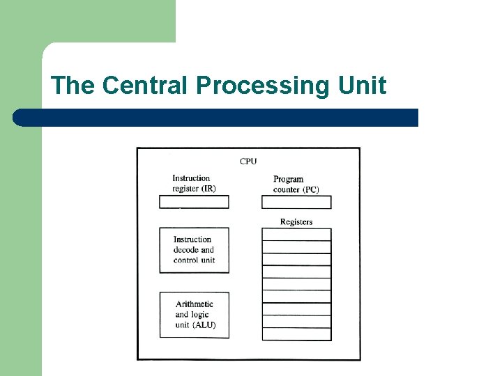
The Central Processing Unit l Contents of the CPU: – – Registers: Store information and set operational parameters. Arithmetic Unit (ALU): Perform operations on registers. Instruction Decode and Control Unit: Determines operations to perform and set in motion necessary actions. Program Counter: Holds the memory address of the NEXT instruction to be processed.

The Central Processing Unit

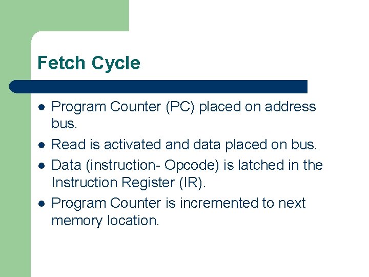
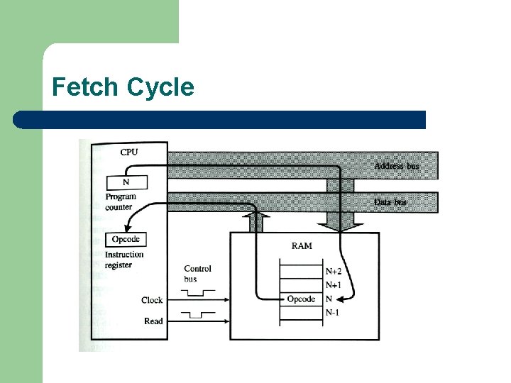
Fetch Cycle l l Program Counter (PC) placed on address bus. Read is activated and data placed on bus. Data (instruction- Opcode) is latched in the Instruction Register (IR). Program Counter is incremented to next memory location.

Fetch Cycle

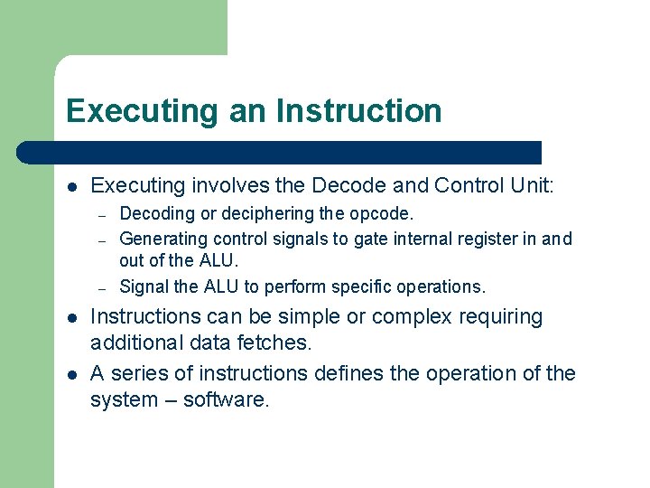
Executing an Instruction l Executing involves the Decode and Control Unit: – – – l l Decoding or deciphering the opcode. Generating control signals to gate internal register in and out of the ALU. Signal the ALU to perform specific operations. Instructions can be simple or complex requiring additional data fetches. A series of instructions defines the operation of the system – software.

Microcontrollers l Differ from microprocessors in: – – – Hardware Architecture Applications Instruction Set Features

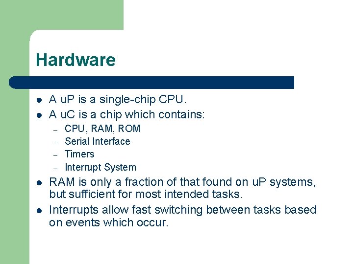
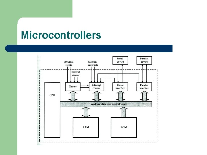
Hardware l l A u. P is a single-chip CPU. A u. C is a chip which contains: – – l l CPU, RAM, ROM Serial Interface Timers Interrupt System RAM is only a fraction of that found on u. P systems, but sufficient for most intended tasks. Interrupts allow fast switching between tasks based on events which occur.

Microcontrollers

Microcontroller Applications l l l Microcontrollers are well suited for systems that require a small component count. Applications are relatively small and suited to very precise tasks. Relatively simple I/O control.

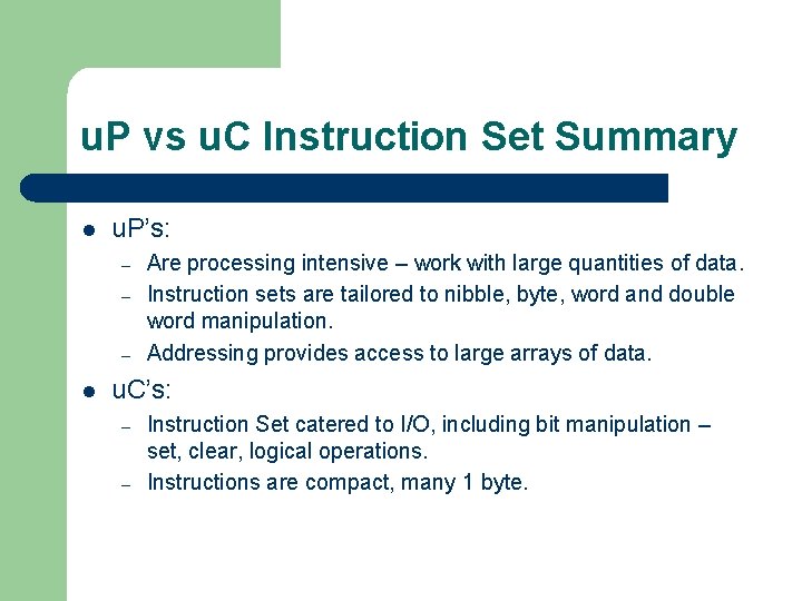
u. P vs u. C Instruction Set Summary l u. P’s: – – – l Are processing intensive – work with large quantities of data. Instruction sets are tailored to nibble, byte, word and double word manipulation. Addressing provides access to large arrays of data. u. C’s: – – Instruction Set catered to I/O, including bit manipulation – set, clear, logical operations. Instructions are compact, many 1 byte.

Memory Comparisons l l Computer have a large RAM to ROM ratio for O/S, applications and data. u. C’s have a large ROM to RAM ratio since programs are stored on ROM and very little data storage is typical.

Overview of the 8051 Family l l l One of the oldest (Intel MCS-51 in 1980) and probably the most popular microcontroller. Many derivatives are marketed by a number of vendors. Common features, – 8 -bit processor – 4 I/O ports each 8 bits wide – max of 64 K on-chip ROM (usually 0 k to 4 k) – max of 64 K external data memory – max of 64 K external code memory – 2 timers, one serial port – 128 bytes of on-chip RAM – various speeds from 12 MHz Clones may have different on-chip memory, timers

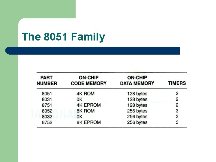
The 8051 Family

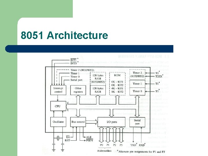
8051 Architecture

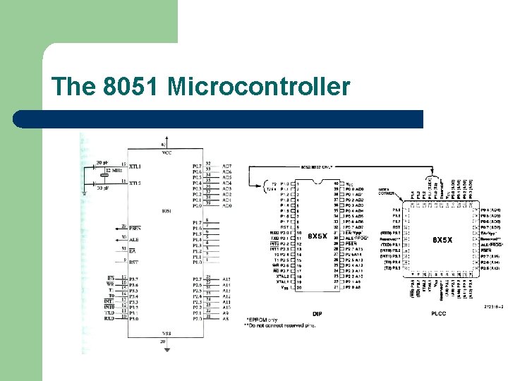
The 8051 Microcontroller

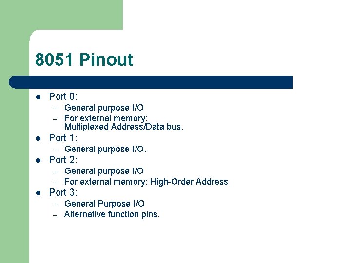
8051 Pinout l Port 0: – – l Port 1: – l General purpose I/O. Port 2: – – l General purpose I/O For external memory: Multiplexed Address/Data bus. General purpose I/O For external memory: High-Order Address Port 3: – – General Purpose I/O Alternative function pins.

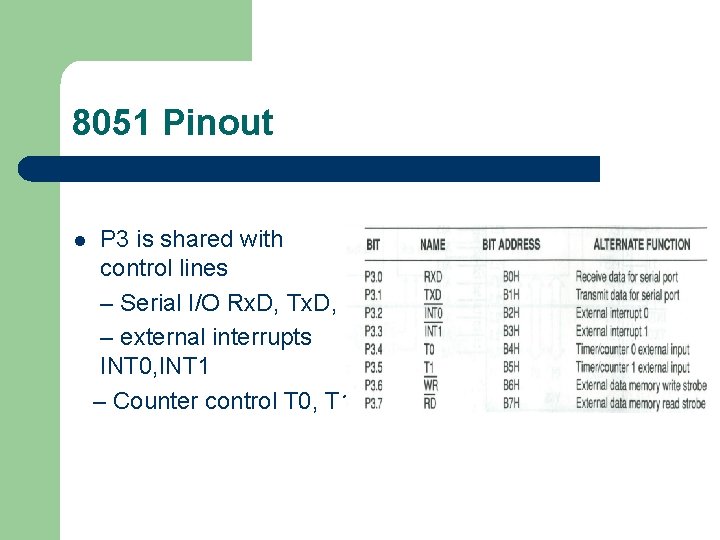
8051 Pinout l P 3 is shared with control lines – Serial I/O Rx. D, Tx. D, – external interrupts INT 0, INT 1 – Counter control T 0, T 1

8051 Pinout l External device interfacing – EA - External Access (L for ext Memory) – ALE - Address Latch Enable – PSEN – Program Store Enable – WR – Write Enable – RD – Read Enable

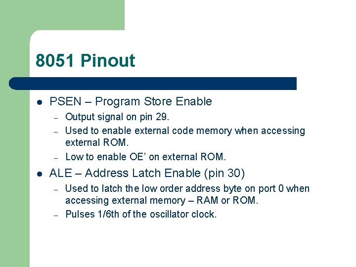
8051 Pinout l PSEN – Program Store Enable – – – l Output signal on pin 29. Used to enable external code memory when accessing external ROM. Low to enable OE’ on external ROM. ALE – Address Latch Enable (pin 30) – – Used to latch the low order address byte on port 0 when accessing external memory – RAM or ROM. Pulses 1/6 th of the oscillator clock.

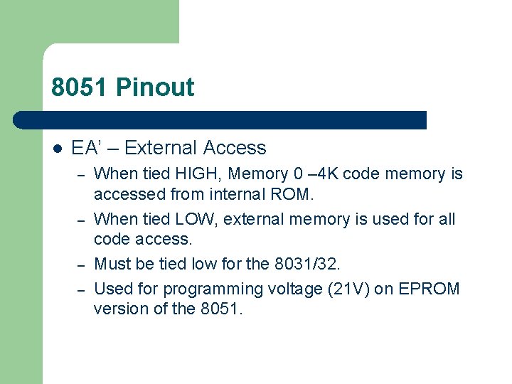
8051 Pinout l EA’ – External Access – – When tied HIGH, Memory 0 – 4 K code memory is accessed from internal ROM. When tied LOW, external memory is used for all code access. Must be tied low for the 8031/32. Used for programming voltage (21 V) on EPROM version of the 8051.

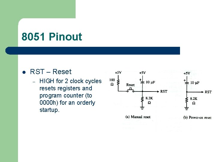
8051 Pinout l RST – Reset – HIGH for 2 clock cycles resets registers and program counter (to 0000 h) for an orderly startup.

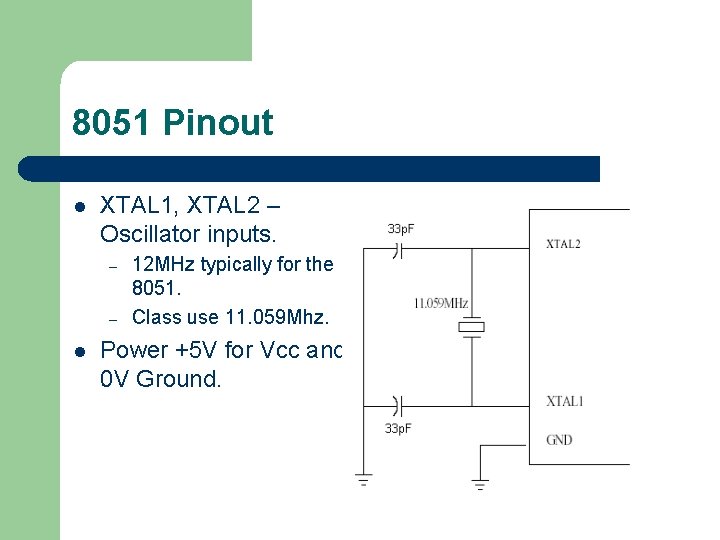
8051 Pinout l XTAL 1, XTAL 2 – Oscillator inputs. – – l 12 MHz typically for the 8051. Class use 11. 059 Mhz. Power +5 V for Vcc and 0 V Ground.

Memory Organization l l l Separate memory for code and data. Internal (4 K) and/or external (64 K) ROM for code. On-chip RAM: – – l l General purpose storage Bit-addressable storage Register banks Special Function Registers (SFRs) I/O ports are memory mapped directly to SFR RAM locations. Stack resides within internal RAM.

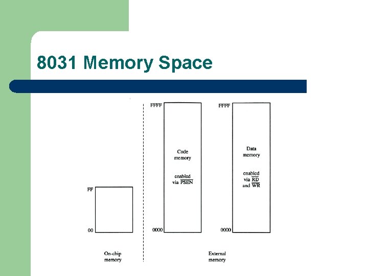
8031 Memory Space

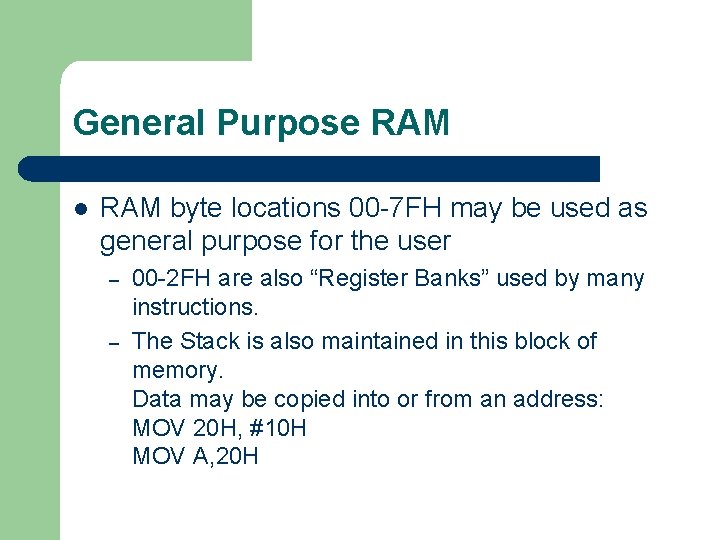
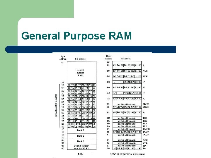
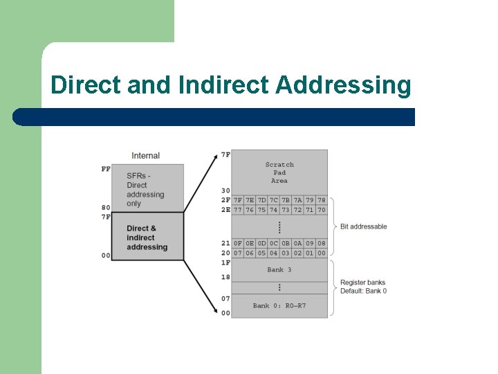
General Purpose RAM l RAM byte locations 00 -7 FH may be used as general purpose for the user – – 00 -2 FH are also “Register Banks” used by many instructions. The Stack is also maintained in this block of memory. Data may be copied into or from an address: MOV 20 H, #10 H MOV A, 20 H

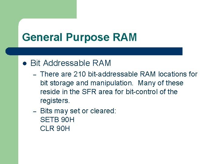
General Purpose RAM l Bit Addressable RAM – – There are 210 bit-addressable RAM locations for bit storage and manipulation. Many of these reside in the SFR area for bit-control of the registers. Bits may set or cleared: SETB 90 H CLR 90 H

General Purpose RAM

Direct and Indirect Addressing

Direct Addressing of the Special Function Register (SFR)

Register Banks l l l RAM locations 00 to 1 FH (32 bytes) are 4 Register banks, each with 8 bytes named R 0 -R 7. An instruction using a register bank may be performed with less code and faster than other instructions (1 byte vice 2). MOV R 0, A R 0 implies 1 of 4 bytes dependent on which bank is selected. This allows different section of programs to use the register banks for their own purposes without conflict.

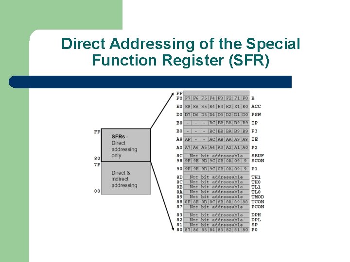
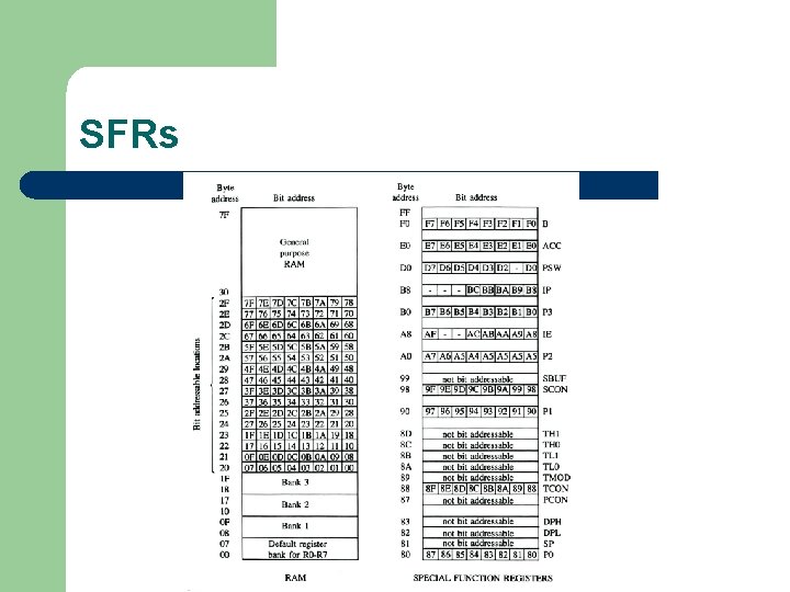
Special Function Registers (SFRs) l l Internal registers are made part of RAM for direct access and bit manipulation. These registers are manipulated either through the instruction set or directly for processor control.

SFRs

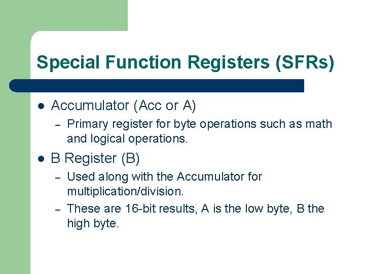
Special Function Registers (SFRs) l Accumulator (Acc or A) – l Primary register for byte operations such as math and logical operations. B Register (B) – – Used along with the Accumulator for multiplication/division. These are 16 -bit results, A is the low byte, B the high byte.

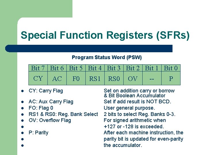
Special Function Registers (SFRs) Program Status Word (PSW) Bit 7 Bit 6 Bit 5 Bit 4 Bit 3 Bit 2 Bit 1 Bit 0 CY AC F 0 RS 1 RS 0 OV -P l CY: Carry Flag l AC: Aux Carry Flag FO: Flag 0 RS 1 & RS 0: Reg. Bank Select OV: Overflow Flag l l l l P: Parity Set on addition carry or borrow & Bit Boolean Accumulator Set if add result is NOT BCD. User general purpose. 2 bits to select Reg. Banks 0 -3. For signed arithmetic when +127 or -128 is exceeded. After each machine instruction, the parity bit is updated for even-parity the accumulator.

Special Function Registers (SFRs) l Stack Pointer (SP) – – – Points to the address of top of the ‘stack’. Addresses and data are ‘pushed’ onto the stack and ‘popped’ off, last-in, first-out (LIFO). The stack is incremented prior to pushing. The reset value of SP is 07 F which would over-run the register bank area. (its incremented before use to 08 H) If the SP is not reinitialized register banks 1 (maybe 2 and 3) might not be available for use.

Special Function Registers (SFRs) l Data Pointer (DPTR) – – 16 -bit register used to address external RAM. The 16 -bit address is place on Ports 0 and 2. RD and WR I/O’s are used to determine data direction. Data is moved on Port 0

Special Function Registers (SFRs) l Port Registers – – All port registers are directly byte and bit addressable. Configuration of external memory may limit use of these ports 0, 2 and 3 for general use.

Special Function Registers (SFRs) l Timer Registers – – Two 16 -bit registers are used for timers or counters. Other applicable registers for these operations are TCON and TMOD

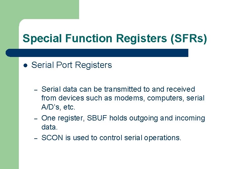
Special Function Registers (SFRs) l Serial Port Registers – – – Serial data can be transmitted to and received from devices such as modems, computers, serial A/D’s, etc. One register, SBUF holds outgoing and incoming data. SCON is used to control serial operations.

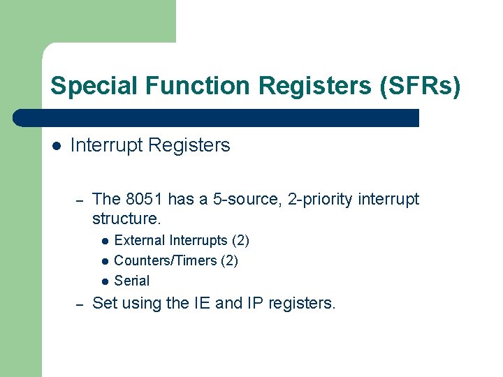
Special Function Registers (SFRs) l Interrupt Registers – The 8051 has a 5 -source, 2 -priority interrupt structure. l l l – External Interrupts (2) Counters/Timers (2) Serial Set using the IE and IP registers.

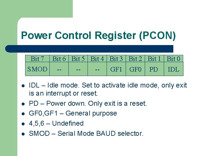
Power Control Register (PCON) Bit 7 Bit 6 Bit 5 Bit 4 Bit 3 Bit 2 Bit 1 Bit 0 SMOD ---GF 1 GF 0 PD IDL l l l IDL – Idle mode. Set to activate idle mode, only exit is an interrupt or reset. PD – Power down. Only exit is a reset. GF 0, GF 1 – General purpose 4, 5, 6 – Undefined SMOD – Serial Mode BAUD selector.

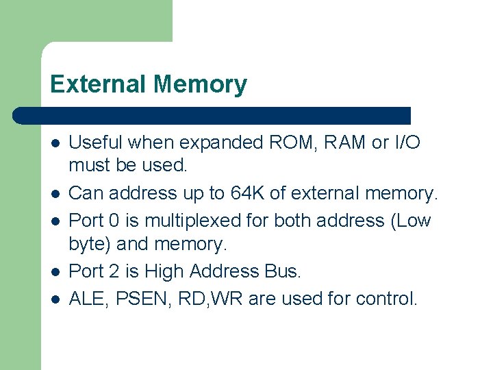
External Memory l l l Useful when expanded ROM, RAM or I/O must be used. Can address up to 64 K of external memory. Port 0 is multiplexed for both address (Low byte) and memory. Port 2 is High Address Bus. ALE, PSEN, RD, WR are used for control.

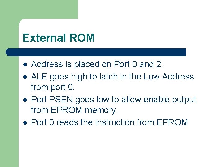
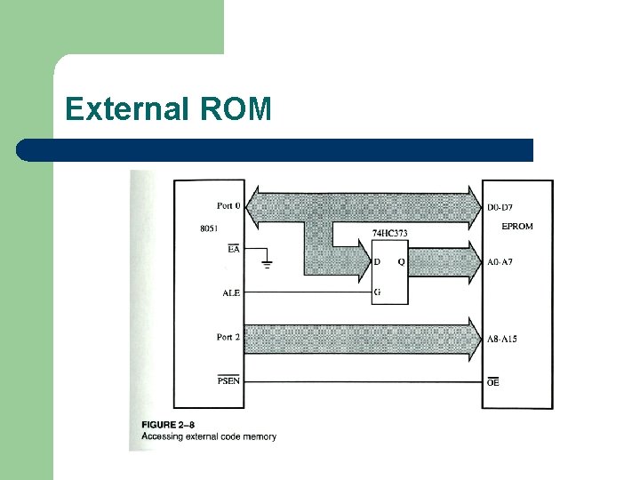
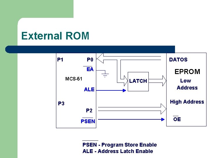
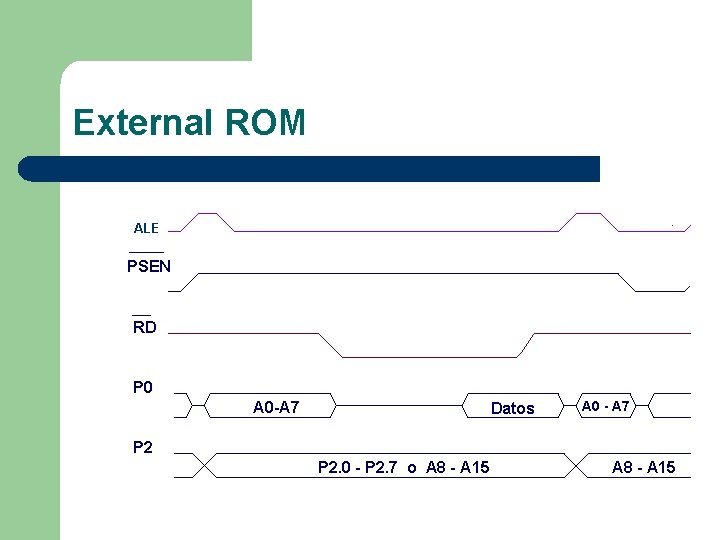
External ROM l l Address is placed on Port 0 and 2. ALE goes high to latch in the Low Address from port 0. Port PSEN goes low to allow enable output from EPROM memory. Port 0 reads the instruction from EPROM

External ROM

External ROM P 1 P 0 DATOS EA MCS-51 EPROM LATCH ALE Low Address High Address P 3 P 2 PSEN - Program Store Enable ALE - Address Latch Enable OE

External ROM ALE PSEN RD P 0 A 0 -A 7 Datos A 0 - A 7 P 2. 0 - P 2. 7 o A 8 - A 15

External RAM l External RAM memory location can be accessed using MOVX instruction: – – The DPTR register for 64 K access. Using RO or R 1 for 256 byte access – Frees Port 2 for other uses.

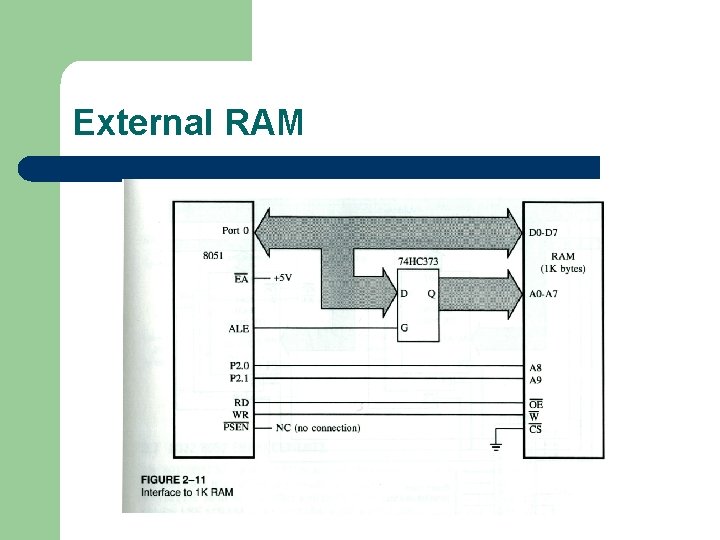
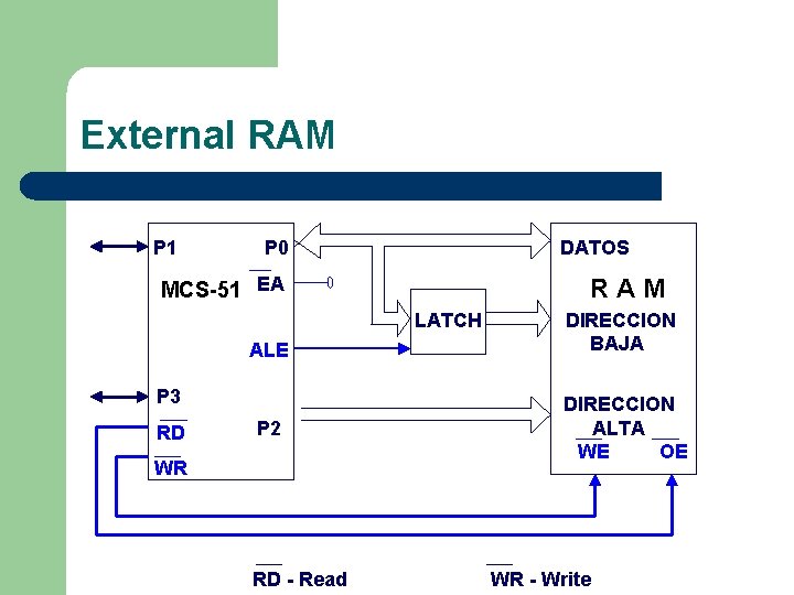
External RAM l l l Address is placed on Port 0 (and port 2). ALE latches in low address. For writing: – – l Data is placed on Port 0 WR goes to write to RAM For reading: – – RD goes low to enable RAM output. Port 0 Reads data.

External RAM

External RAM P 1 P 0 DATOS MCS-51 EA RAM LATCH ALE P 3 RD P 2 WR RD - Read DIRECCION BAJA DIRECCION ALTA WE OE WR - Write