Lecture 14 Wires Outline q Introduction q Interconnect
![Example Intel 90 nm Stack Intel 45 nm Stack [Thompson 02] 14: Wires [Moon Example Intel 90 nm Stack Intel 45 nm Stack [Thompson 02] 14: Wires [Moon](https://slidetodoc.com/presentation_image_h/902ff1d811adb49f92ff0eaf2594cc6b/image-6.jpg)


- Slides: 83

Lecture 14: Wires

Outline q Introduction q Interconnect Modeling – Wire Resistance – Wire Capacitance q Wire RC Delay q Crosstalk q Wire Engineering q Repeaters 14: Wires CMOS VLSI Design 4 th Ed. 2

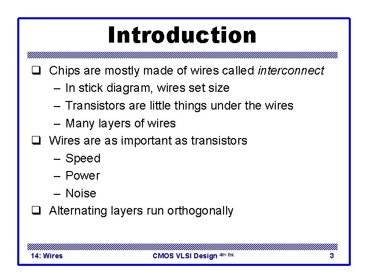
Introduction q Chips are mostly made of wires called interconnect – In stick diagram, wires set size – Transistors are little things under the wires – Many layers of wires q Wires are as important as transistors – Speed – Power – Noise q Alternating layers run orthogonally 14: Wires CMOS VLSI Design 4 th Ed. 3

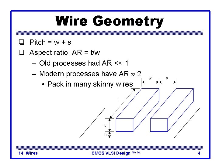
Wire Geometry q Pitch = w + s q Aspect ratio: AR = t/w – Old processes had AR << 1 – Modern processes have AR 2 • Pack in many skinny wires 14: Wires CMOS VLSI Design 4 th Ed. 4

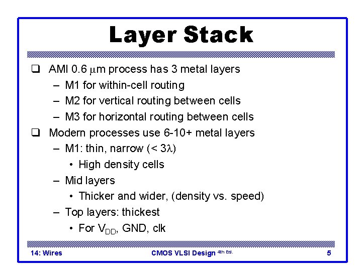
Layer Stack q AMI 0. 6 mm process has 3 metal layers – M 1 for within-cell routing – M 2 for vertical routing between cells – M 3 for horizontal routing between cells q Modern processes use 6 -10+ metal layers – M 1: thin, narrow (< 3 l) • High density cells – Mid layers • Thicker and wider, (density vs. speed) – Top layers: thickest • For VDD, GND, clk 14: Wires CMOS VLSI Design 4 th Ed. 5
![Example Intel 90 nm Stack Intel 45 nm Stack Thompson 02 14 Wires Moon Example Intel 90 nm Stack Intel 45 nm Stack [Thompson 02] 14: Wires [Moon](https://slidetodoc.com/presentation_image_h/902ff1d811adb49f92ff0eaf2594cc6b/image-6.jpg)
Example Intel 90 nm Stack Intel 45 nm Stack [Thompson 02] 14: Wires [Moon 08] CMOS VLSI Design 4 th Ed. 6

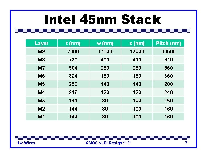
Intel 45 nm Stack Layer t (nm) w (nm) s (nm) Pitch (nm) M 9 7000 17500 13000 30500 M 8 720 400 410 810 M 7 504 280 560 M 6 324 180 360 M 5 252 140 280 M 4 216 120 240 M 3 144 80 100 160 M 2 144 80 100 160 M 1 144 80 100 160 14: Wires CMOS VLSI Design 4 th Ed. 7

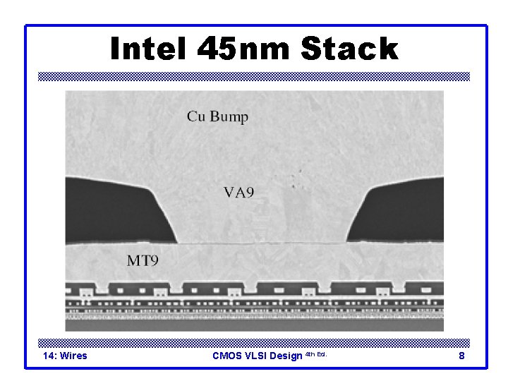
Intel 45 nm Stack 14: Wires CMOS VLSI Design 4 th Ed. 8

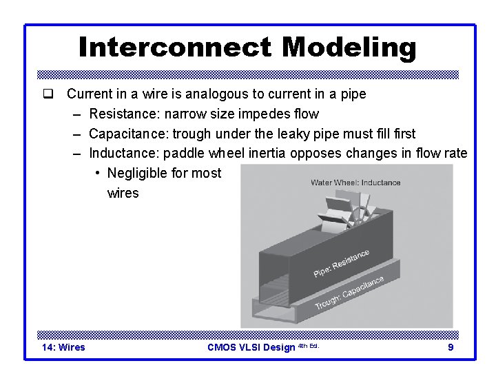
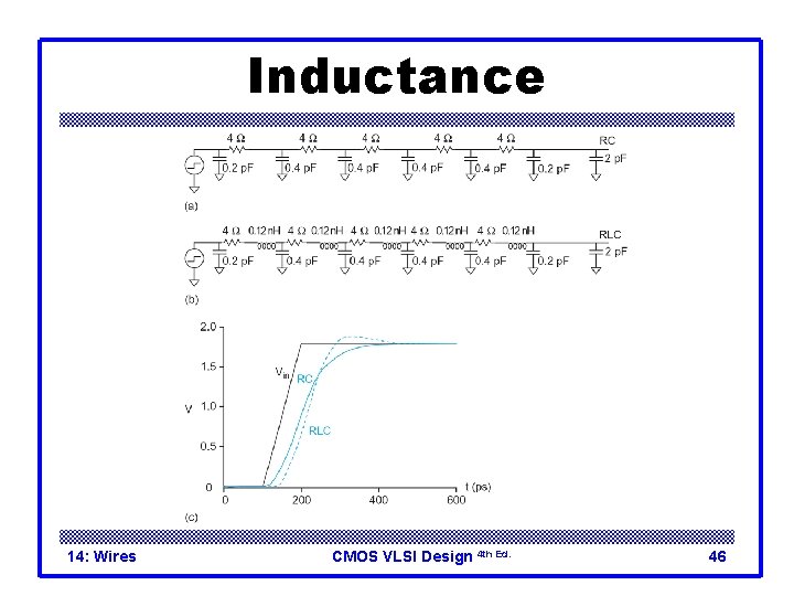
Interconnect Modeling q Current in a wire is analogous to current in a pipe – Resistance: narrow size impedes flow – Capacitance: trough under the leaky pipe must fill first – Inductance: paddle wheel inertia opposes changes in flow rate • Negligible for most wires 14: Wires CMOS VLSI Design 4 th Ed. 9

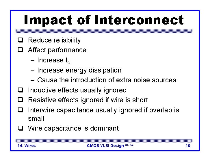
Impact of Interconnect q Reduce reliability q Affect performance – Increase tp – Increase energy dissipation – Cause the introduction of extra noise sources q Inductive effects usually ignored q Resistive effects ignored if wire is short q Interwire capacitance usually ignored if overlap is small q Wire capacitance is dominant 14: Wires CMOS VLSI Design 4 th Ed. 10

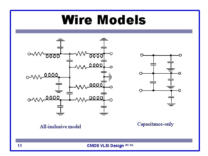
Wire Models Capacitance-only All-inclusive model 11 CMOS VLSI Design 4 th Ed.

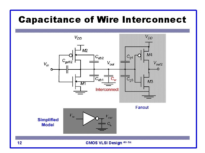
Capacitance of Wire Interconnect 12 CMOS VLSI Design 4 th Ed.

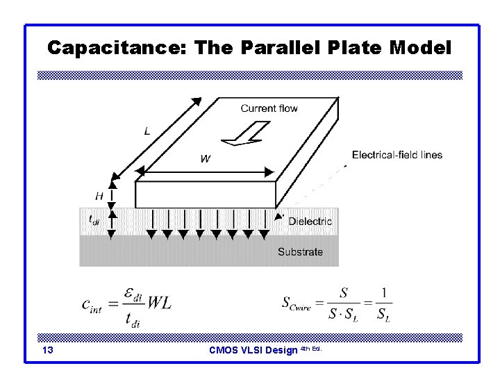
Capacitance: The Parallel Plate Model 13 CMOS VLSI Design 4 th Ed.

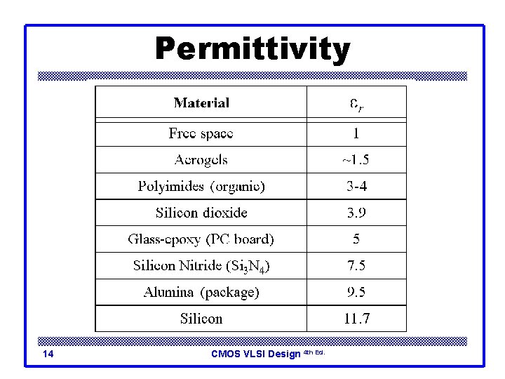
Permittivity 14 CMOS VLSI Design 4 th Ed.

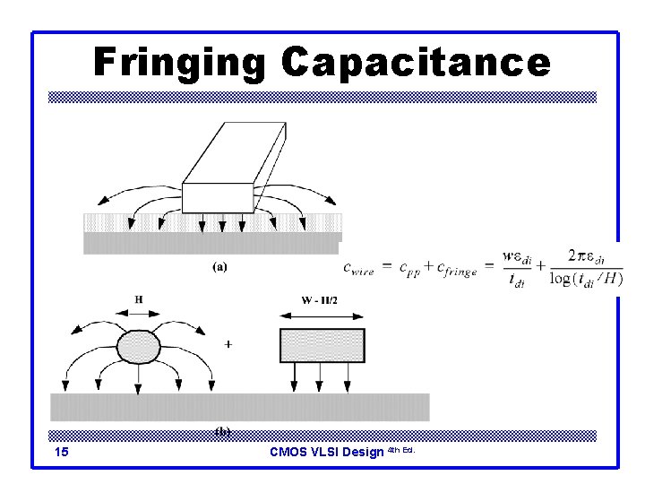
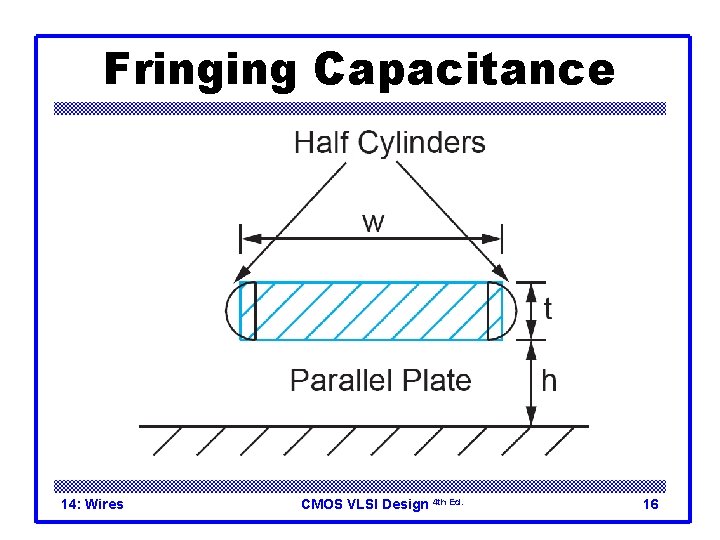
Fringing Capacitance 15 CMOS VLSI Design 4 th Ed.

Fringing Capacitance 14: Wires CMOS VLSI Design 4 th Ed. 16

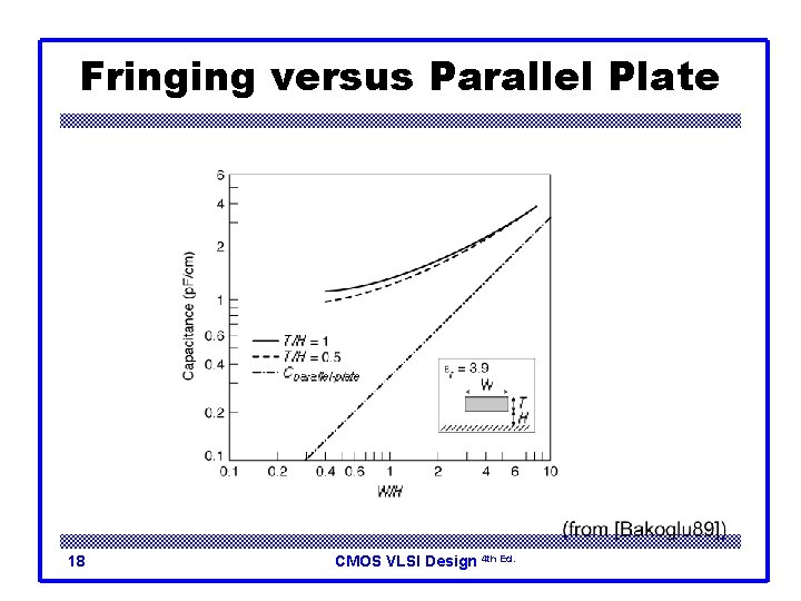
Fringing Capacitance q Some other formulas q This empirical formula is accurate to 6% for AR < 3. 3 14: Wires CMOS VLSI Design 4 th Ed. 17

Fringing versus Parallel Plate 18 CMOS VLSI Design 4 th Ed.

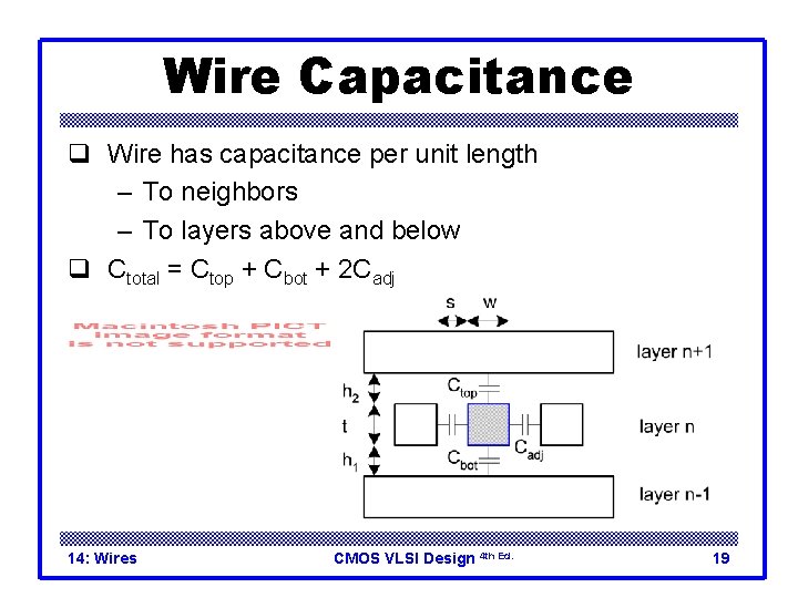
Wire Capacitance q Wire has capacitance per unit length – To neighbors – To layers above and below q Ctotal = Ctop + Cbot + 2 Cadj 14: Wires CMOS VLSI Design 4 th Ed. 19

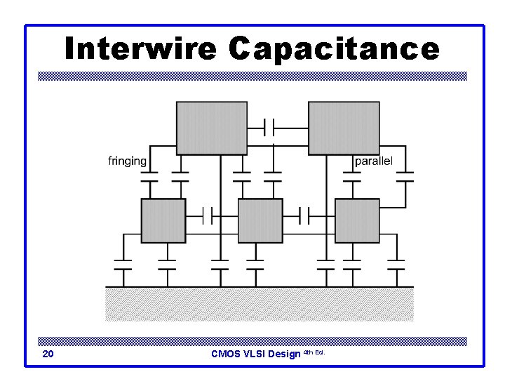
Interwire Capacitance 20 CMOS VLSI Design 4 th Ed.

Capacitance Trends q Parallel plate equation: C = eox. A/d – Wires are not parallel plates, but obey trends – Increasing area (W, t) increases capacitance – Increasing distance (s, h) decreases capacitance q Dielectric constant – eox = ke 0 • e 0 = 8. 85 x 10 -14 F/cm • k = 3. 9 for Si. O 2 q Processes are starting to use low-k dielectrics – k 3 (or less) as dielectrics use air pockets 14: Wires CMOS VLSI Design 4 th Ed. 21

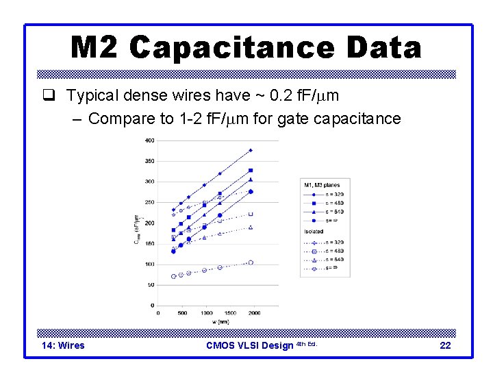
M 2 Capacitance Data q Typical dense wires have ~ 0. 2 f. F/mm – Compare to 1 -2 f. F/mm for gate capacitance 14: Wires CMOS VLSI Design 4 th Ed. 22

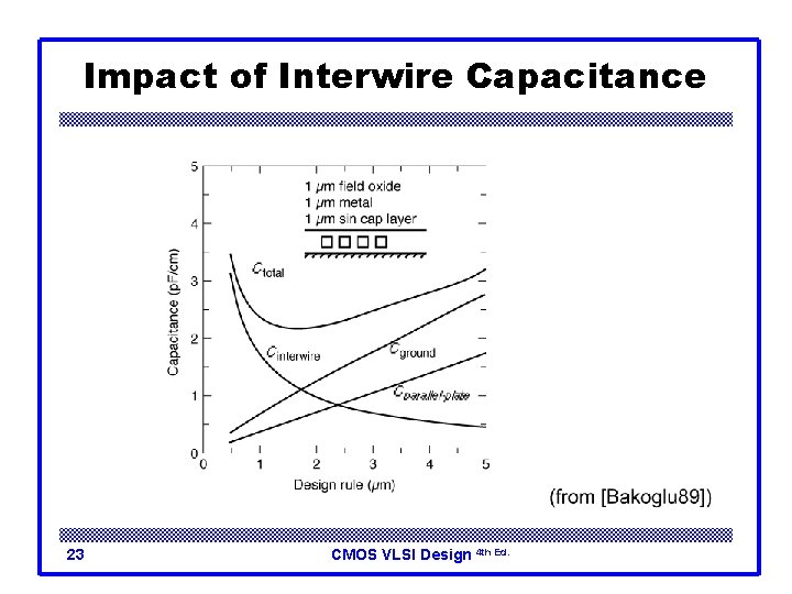
Impact of Interwire Capacitance 23 CMOS VLSI Design 4 th Ed.

Capacitance of Dense Wires q An empirical equation is q Also, floating capacitors occur, which – Create noise – Affect performance 14: Wires CMOS VLSI Design 4 th Ed. 24

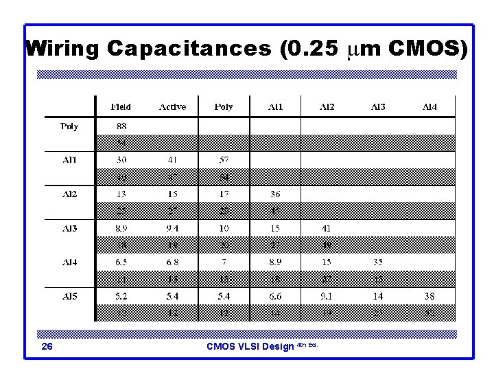
Wiring Capacitances q We typically use simple models for capacitance, given by 14: Wires CMOS VLSI Design 4 th Ed. 25

Wiring Capacitances (0. 25 mm CMOS) 26 CMOS VLSI Design 4 th Ed.

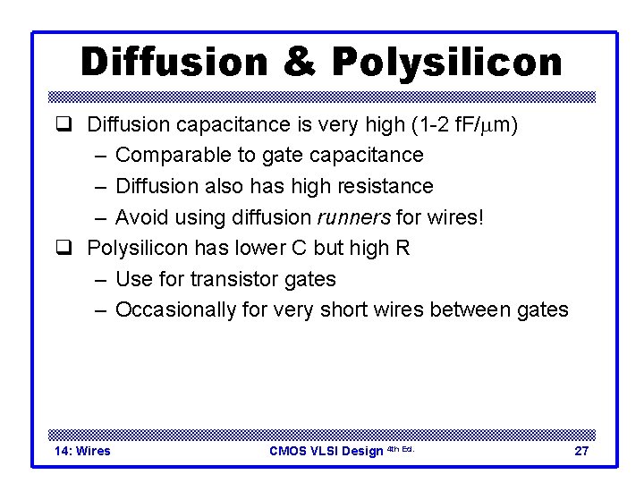
Diffusion & Polysilicon q Diffusion capacitance is very high (1 -2 f. F/mm) – Comparable to gate capacitance – Diffusion also has high resistance – Avoid using diffusion runners for wires! q Polysilicon has lower C but high R – Use for transistor gates – Occasionally for very short wires between gates 14: Wires CMOS VLSI Design 4 th Ed. 27

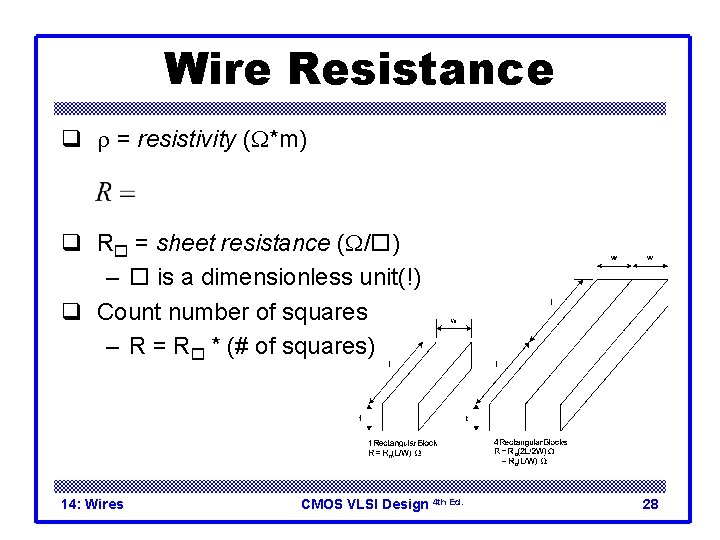
Wire Resistance q r = resistivity (W*m) q R = sheet resistance (W/ ) – is a dimensionless unit(!) q Count number of squares – R = R * (# of squares) 14: Wires CMOS VLSI Design 4 th Ed. 28

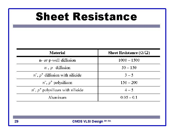
Sheet Resistance 29 CMOS VLSI Design 4 th Ed.

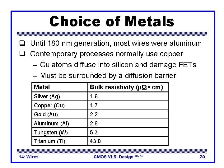
Choice of Metals q Until 180 nm generation, most wires were aluminum q Contemporary processes normally use copper – Cu atoms diffuse into silicon and damage FETs – Must be surrounded by a diffusion barrier Metal Bulk resistivity (m. W • cm) Silver (Ag) 1. 6 Copper (Cu) 1. 7 Gold (Au) 2. 2 Aluminum (Al) 2. 8 Tungsten (W) 5. 3 Titanium (Ti) 43. 0 14: Wires CMOS VLSI Design 4 th Ed. 30

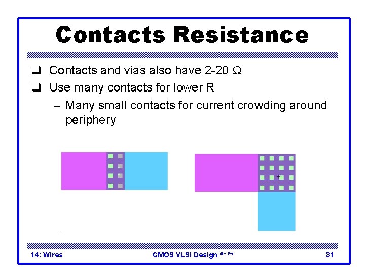
Contacts Resistance q Contacts and vias also have 2 -20 W q Use many contacts for lower R – Many small contacts for current crowding around periphery 14: Wires CMOS VLSI Design 4 th Ed. 31

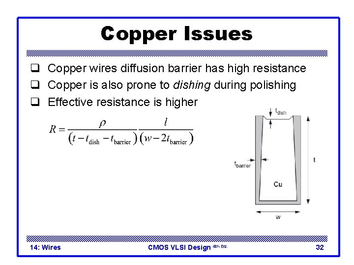
Copper Issues q Copper wires diffusion barrier has high resistance q Copper is also prone to dishing during polishing q Effective resistance is higher 14: Wires CMOS VLSI Design 4 th Ed. 32

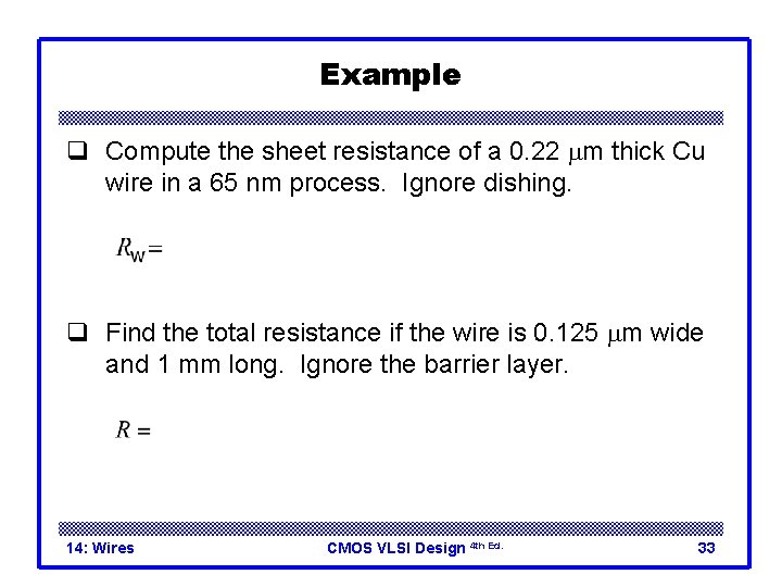
Example q Compute the sheet resistance of a 0. 22 mm thick Cu wire in a 65 nm process. Ignore dishing. q Find the total resistance if the wire is 0. 125 mm wide and 1 mm long. Ignore the barrier layer. 14: Wires CMOS VLSI Design 4 th Ed. 33

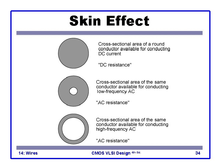
Skin Effect 14: Wires CMOS VLSI Design 4 th Ed. 34

Skin Effect q Define a skin depth, d, where the current falls to 1/e of its nominal value. q Here, m is the permeability of the surrounding dielectric and has a typical value of approximately 4 p X 10 -7 for all dielectrics. q For Al at 1 GHz, d = 2. 6 mm. q To see the effect, assume a rectangular wire. q Assume that the current flows only in the skin as defined above 14: Wires CMOS VLSI Design 4 th Ed. 35

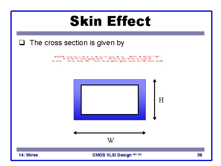
Skin Effect q The cross section is given by H W 14: Wires CMOS VLSI Design 4 th Ed. 36

Skin Effect q Using this cross sectional area, q We can define a frequency fs where the skin depth is half the highest dimension of the conductor. q It is not meaningful to increase the dimensions beyond that point for that frequency. 14: Wires CMOS VLSI Design 4 th Ed. 37

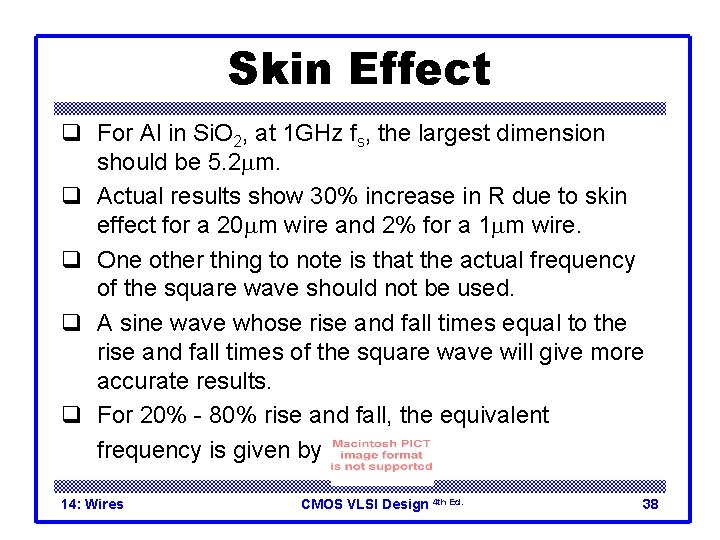
Skin Effect q For Al in Si. O 2, at 1 GHz fs, the largest dimension should be 5. 2 mm. q Actual results show 30% increase in R due to skin effect for a 20 mm wire and 2% for a 1 mm wire. q One other thing to note is that the actual frequency of the square wave should not be used. q A sine wave whose rise and fall times equal to the rise and fall times of the square wave will give more accurate results. q For 20% - 80% rise and fall, the equivalent frequency is given by 14: Wires CMOS VLSI Design 4 th Ed. 38

Skin Effect q As another example, choose copper in Si. O 2 with 20 ps edge rates. q f=5. 8 GHz, d = 0. 99 mm q Note that the resistivity of metals drops at very low temperatures. q For example, an order of magnitude improvement at 77 K (liquid nitrogen). 14: Wires CMOS VLSI Design 4 th Ed. 39

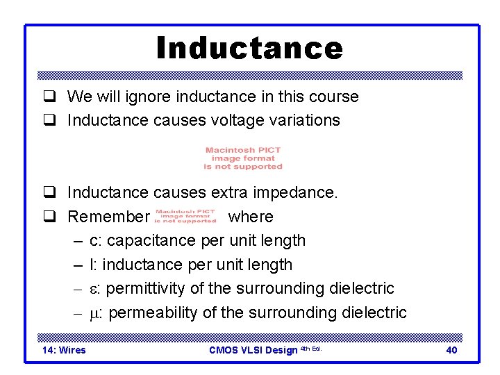
Inductance q We will ignore inductance in this course q Inductance causes voltage variations q Inductance causes extra impedance. q Remember where – c: capacitance per unit length – l: inductance per unit length – e: permittivity of the surrounding dielectric – m: permeability of the surrounding dielectric 14: Wires CMOS VLSI Design 4 th Ed. 40

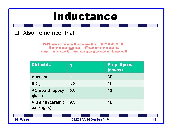
Inductance q Also, remember that 14: Wires Dielectric er Prop. Speed (cm/ns) Vacuum 1 30 Si. O 2 3. 9 15 PC Board (epoxy glass) 5. 0 13 Alumina (ceramic packages) 9. 5 10 CMOS VLSI Design 4 th Ed. 41

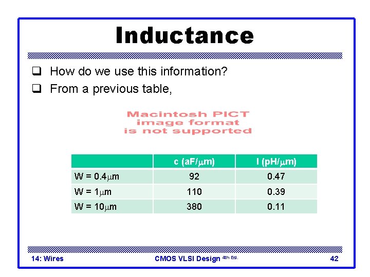
Inductance q How do we use this information? q From a previous table, 14: Wires c (a. F/mm) l (p. H/mm) W = 0. 4 mm 92 0. 47 W = 1 mm 110 0. 39 W = 10 mm 380 0. 11 CMOS VLSI Design 4 th Ed. 42

Inductance q Using q q Equating the impedances, Z = wl For a 1 mm wide wire, r = Z at 30 GHz. Inductance is not an issue for now. Typically, lower level metals are microstrips whose inductances are given by 14: Wires CMOS VLSI Design 4 th Ed. 43

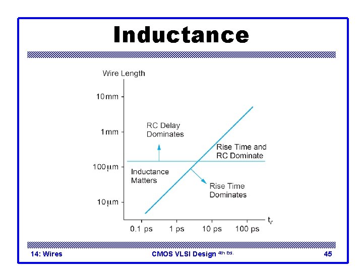
Inductance q On-chip inductance is important for wires where the speed of light flight time is longer than either the rise times of the circuits or the RC delay of the wire. q This can be expressed as 14: Wires CMOS VLSI Design 4 th Ed. 44

Inductance 14: Wires CMOS VLSI Design 4 th Ed. 45

Inductance 14: Wires CMOS VLSI Design 4 th Ed. 46

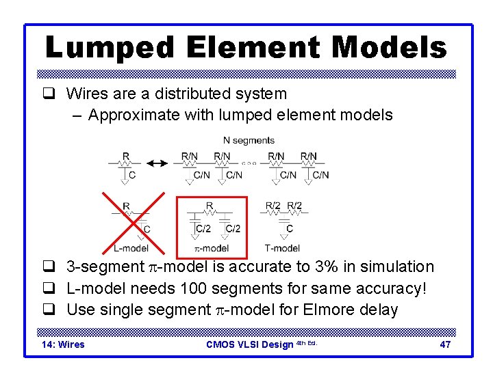
Lumped Element Models q Wires are a distributed system – Approximate with lumped element models q 3 -segment p-model is accurate to 3% in simulation q L-model needs 100 segments for same accuracy! q Use single segment p-model for Elmore delay 14: Wires CMOS VLSI Design 4 th Ed. 47

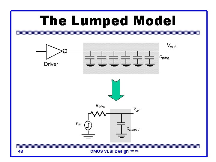
The Lumped Model 48 CMOS VLSI Design 4 th Ed.

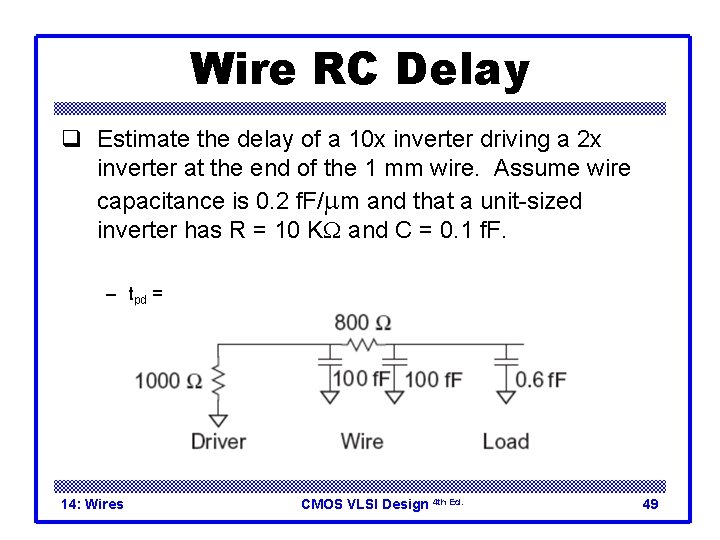
Wire RC Delay q Estimate the delay of a 10 x inverter driving a 2 x inverter at the end of the 1 mm wire. Assume wire capacitance is 0. 2 f. F/mm and that a unit-sized inverter has R = 10 KW and C = 0. 1 f. F. – tpd = (1000 W)(100 f. F) + (1000 + 800 W)(100 + 0. 6 f. F) = 281 ps 14: Wires CMOS VLSI Design 4 th Ed. 49

Wire Energy q Estimate the energy per unit length to send a bit of information (one rising and one falling transition) in a CMOS process. q E = (0. 2 p. F/mm)(1. 0 V)2 14: Wires = 0. 2 p. J/bit/mm = 0. 2 m. W/Gbps CMOS VLSI Design 4 th Ed. 50

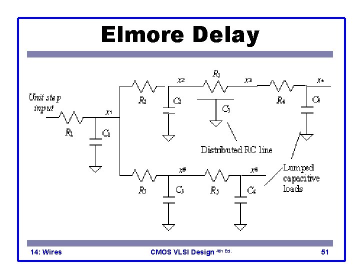
Elmore Delay 14: Wires CMOS VLSI Design 4 th Ed. 51

Elmore Delay 14: Wires CMOS VLSI Design 4 th Ed. 52

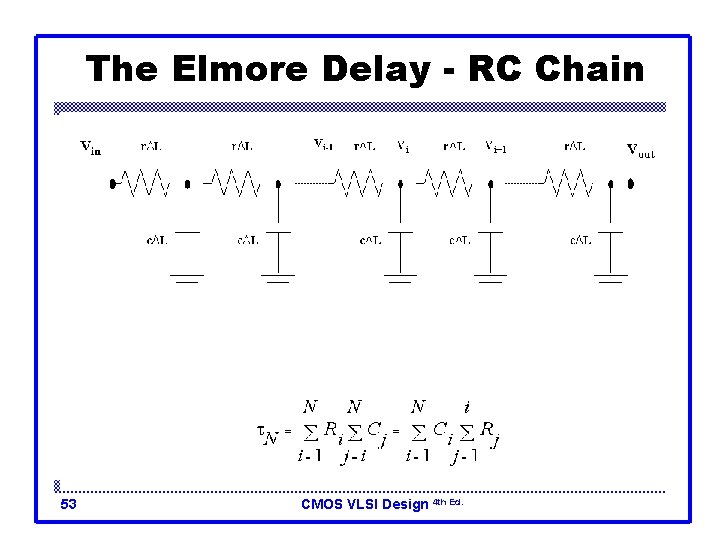
The Elmore Delay - RC Chain 53 CMOS VLSI Design 4 th Ed.

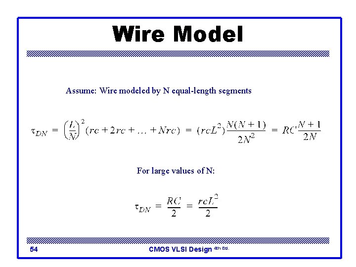
Wire Model Assume: Wire modeled by N equal-length segments For large values of N: 54 CMOS VLSI Design 4 th Ed.

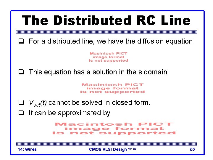
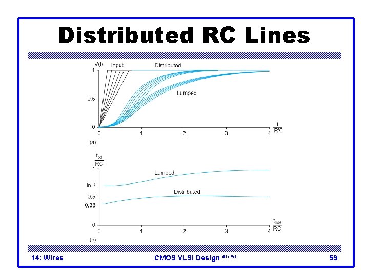
The Distributed RC Line q For a distributed line, we have the diffusion equation q This equation has a solution in the s domain q Vout(t) cannot be solved in closed form. q It can be approximated by 14: Wires CMOS VLSI Design 4 th Ed. 55

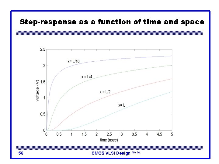
Step-response as a function of time and space 56 CMOS VLSI Design 4 th Ed.

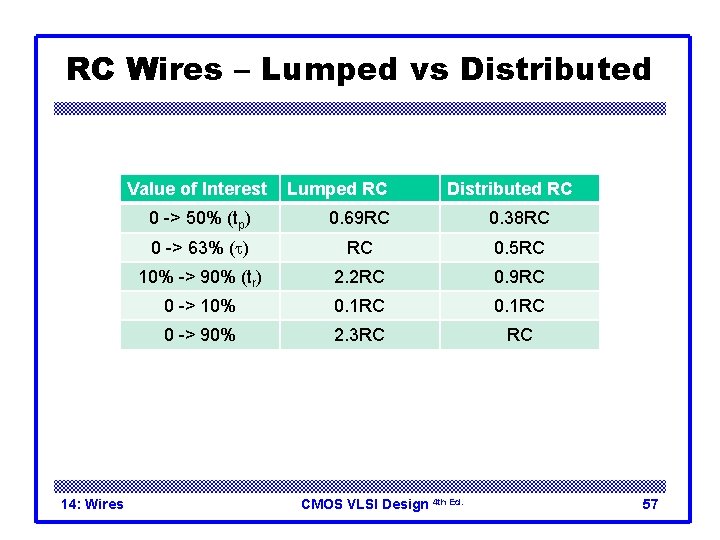
RC Wires – Lumped vs Distributed Value of Interest 14: Wires Lumped RC Distributed RC 0 -> 50% (tp) 0. 69 RC 0. 38 RC 0 -> 63% (t) RC 0. 5 RC 10% -> 90% (tr) 2. 2 RC 0. 9 RC 0 -> 10% 0. 1 RC 0 -> 90% 2. 3 RC RC CMOS VLSI Design 4 th Ed. 57

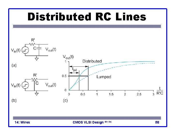
Distributed RC Lines 14: Wires CMOS VLSI Design 4 th Ed. 58

Distributed RC Lines 14: Wires CMOS VLSI Design 4 th Ed. 59

The Transmission Line 14: Wires CMOS VLSI Design 4 th Ed. 60

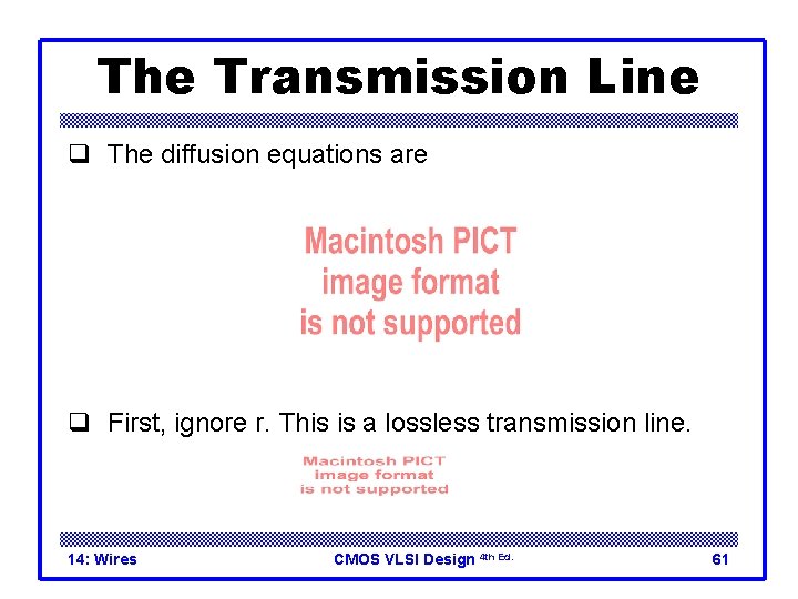
The Transmission Line q The diffusion equations are q First, ignore r. This is a lossless transmission line. 14: Wires CMOS VLSI Design 4 th Ed. 61

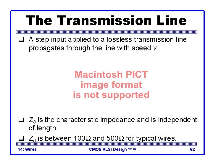
The Transmission Line q A step input applied to a lossless transmission line propagates through the line with speed v. q Z 0 is the characteristic impedance and is independent of length. q Z 0 is between 100 W and 500 W for typical wires. 14: Wires CMOS VLSI Design 4 th Ed. 62

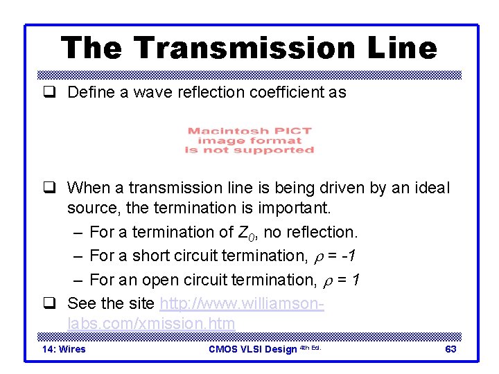
The Transmission Line q Define a wave reflection coefficient as q When a transmission line is being driven by an ideal source, the termination is important. – For a termination of Z 0, no reflection. – For a short circuit termination, r = -1 – For an open circuit termination, r = 1 q See the site http: //www. williamsonlabs. com/xmission. htm 14: Wires CMOS VLSI Design 4 th Ed. 63

The Transmission Line q Case 1: Large source resistance and infinite load resistance. Take RS = 5 Z 0 q Cycle 1: – When this wave reaches the destination, it is fully reflected -> 1. 67 V. – It comes back to the source. The source has become the load. 14: Wires CMOS VLSI Design 4 th Ed. 64

The Transmission Line q Case 1 continued – The new source voltage becomes q We restart the analysis with 1. 1 V for cycle 2. q It is obvious that the signal builds up. q However, the rise time is not determined by any RC constant. It is in terms of number of reflection cycles given by length/velocity. q See the site http: //www. eecs. tufts. edu/~alanh/simulation. html 14: Wires CMOS VLSI Design 4 th Ed. 65

The Transmission Line q Case 2: Small source resistance, infinite load resistance. – Almost all the signal injected into the transmission line. – Reflected from the load. Almost doubles by the time it comes back to the source. – The signal is phase reversed at the source as 14: Wires CMOS VLSI Design 4 th Ed. 66

The Transmission Line q Case 2: The signal exhibits severe ringing. q It takes many cycles before it settles to its final value. q Case 3: Matched source resistance. – Half the signal is injected into the line – Doubles at the termination. – Final value is reached within length/velocity. q Capacitive termination (our case) – No overshoot, behavior asymptotic to t = Z 0 CL – Interesting behavior observed only at source. 14: Wires CMOS VLSI Design 4 th Ed. 67

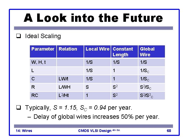
A Look into the Future q Ideal Scaling Parameter Relation Local Wire Constant Length Global Wire W, H, t 1/S 1/S L 1/S 1 1/SC C LW/t 1/S 1 1/SC R L/WH S S 2/SC RC L 2/Ht 1 S 2/S 2 C q Typically, S = 1. 15, SC = 0. 94 per year. – Delay of global wires increases 50% per year. 14: Wires CMOS VLSI Design 4 th Ed. 68

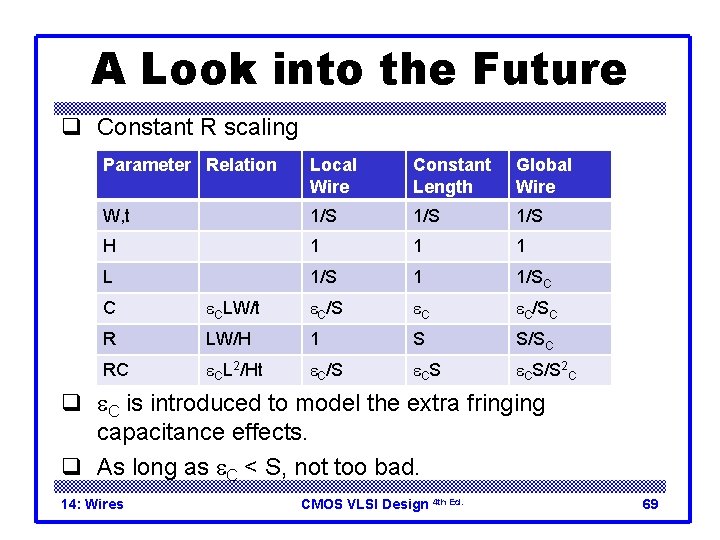
A Look into the Future q Constant R scaling Parameter Relation Local Wire Constant Length Global Wire W, t 1/S 1/S H 1 1 1 L 1/S 1 1/SC C e. CLW/t e. C/SC R LW/H 1 S S/SC RC e. CL 2/Ht e. C/S e. CS/S 2 C q e. C is introduced to model the extra fringing capacitance effects. q As long as e. C < S, not too bad. 14: Wires CMOS VLSI Design 4 th Ed. 69

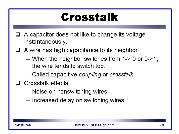
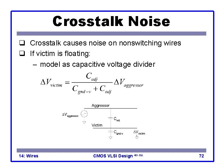
Crosstalk q A capacitor does not like to change its voltage instantaneously. q A wire has high capacitance to its neighbor. – When the neighbor switches from 1 -> 0 or 0 ->1, the wire tends to switch too. – Called capacitive coupling or crosstalk. q Crosstalk effects – Noise on nonswitching wires – Increased delay on switching wires 14: Wires CMOS VLSI Design 4 th Ed. 70

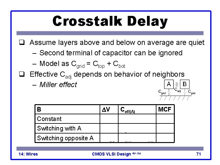
Crosstalk Delay q Assume layers above and below on average are quiet – Second terminal of capacitor can be ignored – Model as Cgnd = Ctop + Cbot q Effective Cadj depends on behavior of neighbors – Miller effect B DV Ceff(A) MCF Constant VDD Cgnd + Cadj 1 Switching with A 0 Cgnd 0 Switching opposite A 2 VDD Cgnd + 2 Cadj 2 14: Wires CMOS VLSI Design 4 th Ed. 71

Crosstalk Noise q Crosstalk causes noise on nonswitching wires q If victim is floating: – model as capacitive voltage divider 14: Wires CMOS VLSI Design 4 th Ed. 72

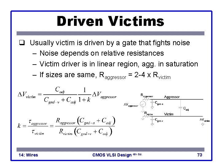
Driven Victims q Usually victim is driven by a gate that fights noise – Noise depends on relative resistances – Victim driver is in linear region, agg. in saturation – If sizes are same, Raggressor = 2 -4 x Rvictim 14: Wires CMOS VLSI Design 4 th Ed. 73

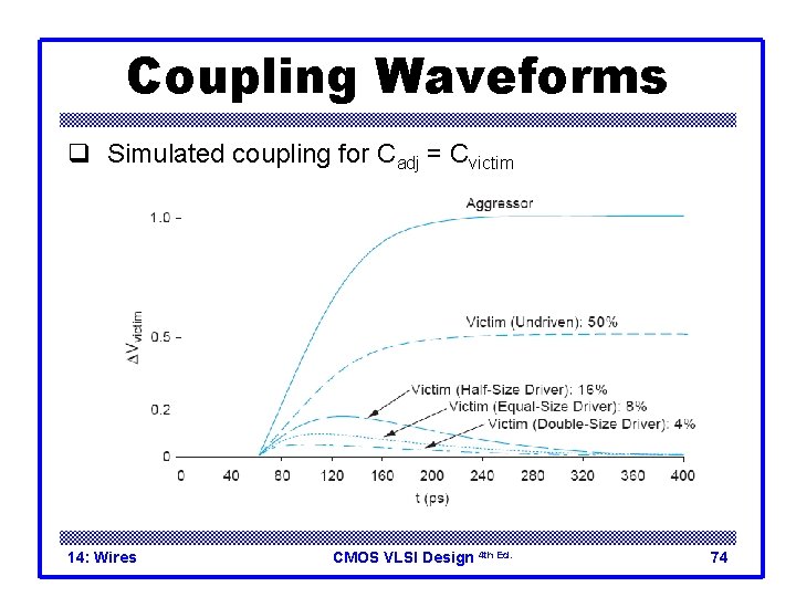
Coupling Waveforms q Simulated coupling for Cadj = Cvictim 14: Wires CMOS VLSI Design 4 th Ed. 74

Noise Implications q So what if we have noise? q If the noise is less than the noise margin, nothing happens q Static CMOS logic will eventually settle to correct output even if disturbed by large noise spikes – But glitches cause extra delay – Also cause extra power from false transitions q Dynamic logic never recovers from glitches q Memories and other sensitive circuits also can produce the wrong answer 14: Wires CMOS VLSI Design 4 th Ed. 75

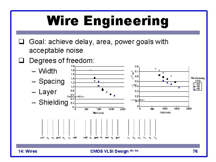
Wire Engineering q Goal: achieve delay, area, power goals with acceptable noise q Degrees of freedom: – Width – Spacing – Layer – Shielding 14: Wires CMOS VLSI Design 4 th Ed. 76

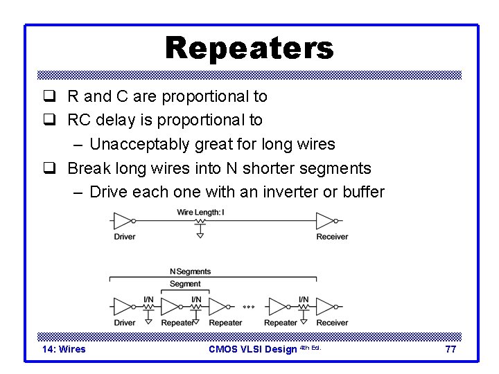
Repeaters q R and C are proportional to l q RC delay is proportional to l 2 – Unacceptably great for long wires q Break long wires into N shorter segments – Drive each one with an inverter or buffer 14: Wires CMOS VLSI Design 4 th Ed. 77

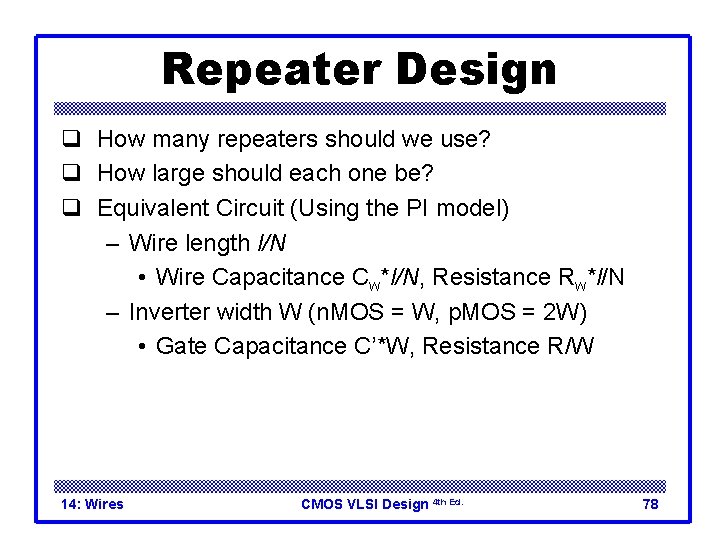
Repeater Design q How many repeaters should we use? q How large should each one be? q Equivalent Circuit (Using the PI model) – Wire length l/N • Wire Capacitance Cw*l/N, Resistance Rw*l/N – Inverter width W (n. MOS = W, p. MOS = 2 W) • Gate Capacitance C’*W, Resistance R/W 14: Wires CMOS VLSI Design 4 th Ed. 78

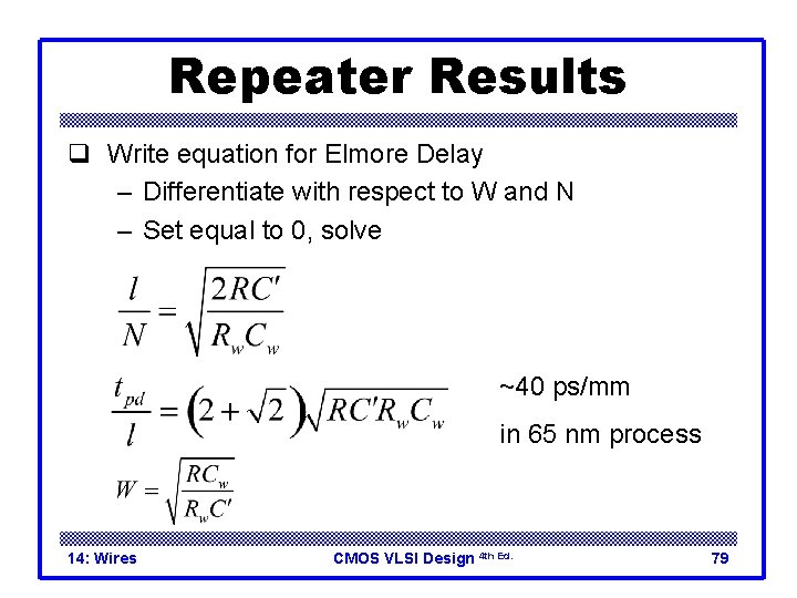
Repeater Results q Write equation for Elmore Delay – Differentiate with respect to W and N – Set equal to 0, solve ~40 ps/mm in 65 nm process 14: Wires CMOS VLSI Design 4 th Ed. 79

Repeater Energy q Energy / length ≈ 1. 87 Cw. VDD 2 – 87% premium over unrepeated wires – The extra power is consumed in the large repeaters q If the repeaters are downsized for minimum EDP: – Energy premium is only 30% – Delay increases by 14% from min delay 14: Wires CMOS VLSI Design 4 th Ed. 80

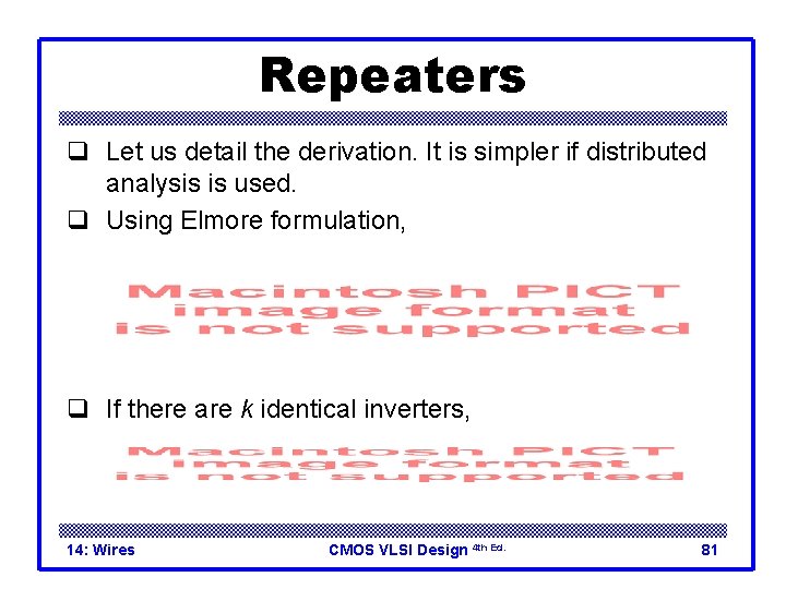
Repeaters q Let us detail the derivation. It is simpler if distributed analysis is used. q Using Elmore formulation, q If there are k identical inverters, 14: Wires CMOS VLSI Design 4 th Ed. 81

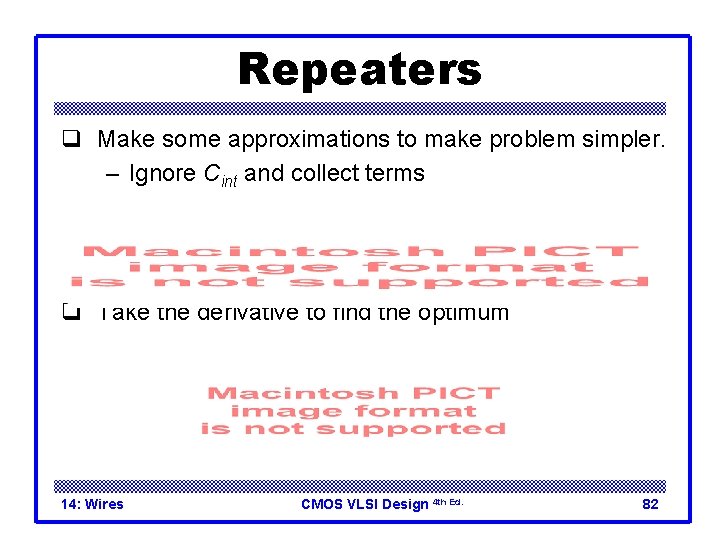
Repeaters q Make some approximations to make problem simpler. – Ignore Cint and collect terms q Take the derivative to find the optimum 14: Wires CMOS VLSI Design 4 th Ed. 82

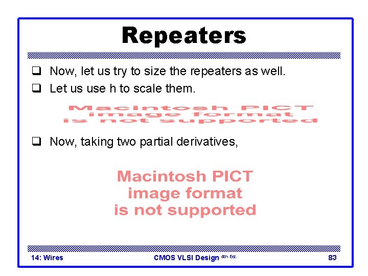
Repeaters q Now, let us try to size the repeaters as well. q Let us use h to scale them. q Now, taking two partial derivatives, 14: Wires CMOS VLSI Design 4 th Ed. 83