OnChip Interconnect Trend and Design Optimization ChungKuan Cheng

![Introduction – Performance Impact n Interconnect delay determines the system performance [ITRS 08] 542 Introduction – Performance Impact n Interconnect delay determines the system performance [ITRS 08] 542](https://slidetodoc.com/presentation_image_h/bb853b2a36b68a66e251c5844b2ff751/image-4.jpg)

- Slides: 84

On-Chip Interconnect Trend and Design Optimization Chung-Kuan Cheng UC San Diego, La Jolla, CA

Outlines • Global Interconnect Technologies – RC Trees and Transmission Lines • Prefix Adder Synthesis – Modeling • FPGA Interconnect Architecture – Modeling • Interconnect Architecture – Non-Manhattan Wire Arrangement 2

Interconnect Technologies • Introduction • On-Chip Global Interconnection • Global Wire Modeling • Performance Comparison 3
![Introduction Performance Impact n Interconnect delay determines the system performance ITRS 08 542 Introduction – Performance Impact n Interconnect delay determines the system performance [ITRS 08] 542](https://slidetodoc.com/presentation_image_h/bb853b2a36b68a66e251c5844b2ff751/image-4.jpg)
Introduction – Performance Impact n Interconnect delay determines the system performance [ITRS 08] 542 ps for 1 mm minimum pitch Cu global wire w/o repeater @ 45 nm ¨ ~150 ps for 10 level FO 4 delay @ 45 nm ¨ [Ho 2001] “Future of Wire” 4

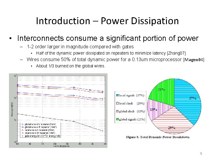
Introduction – Power Dissipation • Interconnects consume a significant portion of power – 1 -2 order larger in magnitude compared with gates • Half of the dynamic power dissipated on repeaters to minimize latency [Zhang 07] – Wires consume 50% of total dynamic power for a 0. 13 um microprocessor [Magen 04] • About 1/3 burned on the global wires. 5

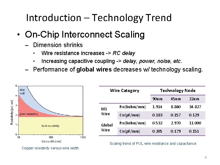
Introduction – Technology Trend • On-Chip Interconnect Scaling – Dimension shrinks • • Wire resistance increases -> RC delay Increasing capacitive coupling -> delay, power, noise, etc. – Performance of global wires decreases w/ technology scaling. Wire Category Technology Node 90 nm 45 nm 22 nm M 1 Wire Rw(kohm/mm) 1. 914 8. 860 34. 827 Cw(p. F/mm) 0. 183 0. 157 0. 129 Global Wire Rw(kohm/mm) 0. 532 2. 970 11. 000 Cw(p. F/mm) 0. 205 0. 179 0. 151 Scaling trend of PUL wire resistance and capacitance Copper resistivity versus wire width 6

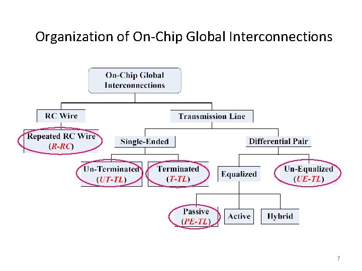
Organization of On-Chip Global Interconnections 7

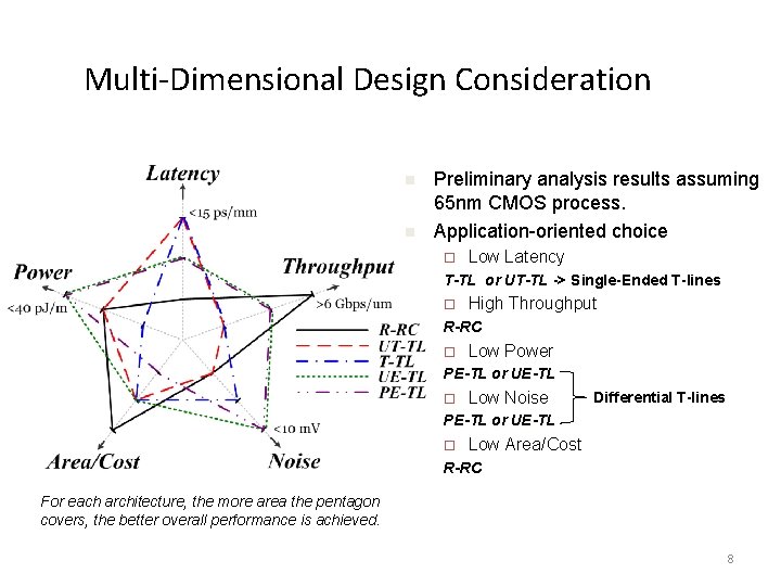
Multi-Dimensional Design Consideration n n Preliminary analysis results assuming 65 nm CMOS process. Application-oriented choice ¨ Low Latency T-TL or UT-TL -> Single-Ended T-lines ¨ High Throughput R-RC ¨ Low Power PE-TL or UE-TL ¨ Low Noise Differential T-lines PE-TL or UE-TL ¨ Low Area/Cost R-RC For each architecture, the more area the pentagon covers, the better overall performance is achieved. 8

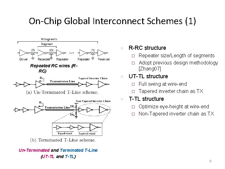
On-Chip Global Interconnect Schemes (1) n R-RC structure Repeater size/Length of segments ¨ Adopt previous design methodology [Zhang 07] ¨ Repeated RC wires (RRC) n UT-TL structure Full swing at wire-end ¨ Tapered inverter chain as TX ¨ n T-TL structure Optimize eye-height at wire-end ¨ Non-Tapered inverter chain as TX ¨ Un-Terminated and Terminated T-Line (UT-TL and T-TL) 9

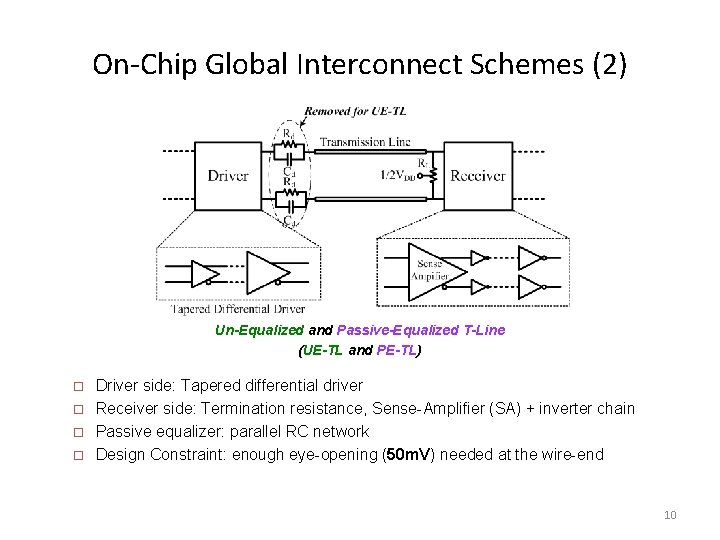
On-Chip Global Interconnect Schemes (2) Un-Equalized and Passive-Equalized T-Line (UE-TL and PE-TL) Driver side: Tapered differential driver ¨ Receiver side: Termination resistance, Sense-Amplifier (SA) + inverter chain ¨ Passive equalizer: parallel RC network ¨ Design Constraint: enough eye-opening (50 m. V) needed at the wire-end ¨ 10

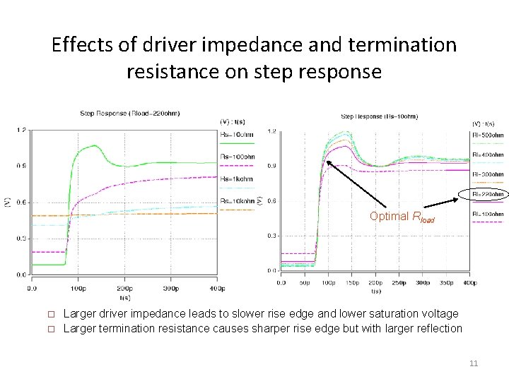
Effects of driver impedance and termination resistance on step response Optimal Rload Larger driver impedance leads to slower rise edge and lower saturation voltage ¨ Larger termination resistance causes sharper rise edge but with larger reflection ¨ 11

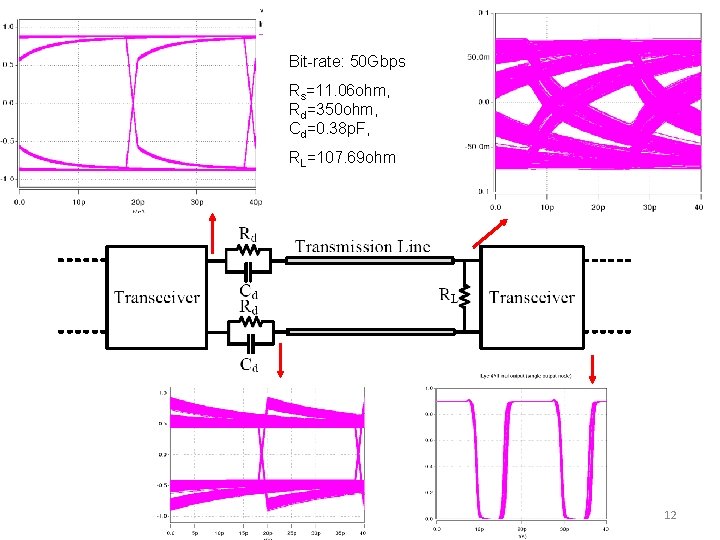
Bit-rate: 50 Gbps Rs=11. 06 ohm, Rd=350 ohm, Cd=0. 38 p. F, RL=107. 69 ohm 12

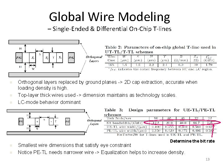
Global Wire Modeling – Single-Ended & Differential On-Chip T-lines n n n Orthogonal layers replaced by ground planes -> 2 D cap extraction, accurate when loading density is high. Top-layer thick wires used -> dimension maintains as technology scales. LC-mode behavior dominant Determine the bit rate Smallest wire dimensions that satisfy eye constraint Notice PE-TL needs narrower wire -> Equalization helps to increase density. 13

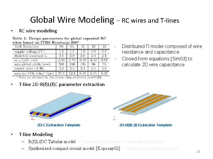
Global Wire Modeling – RC wires and T-lines • RC wire modeling n n • T-line 2 D-R(f)L(f)C parameter extraction 2 D-C Extraction Template • Distributed Π model composed of wire resistance and capacitance Closed-form equations [Sim 03] to calculate 2 D wire capacitance 2 D-R(f)L(f) Extraction Template T-line Modeling – R(f)L(f)C Tabular model -> Transient simulation to estimate eye-height. – Synthesized compact circuit model [Kopcsay 02] -> Study signal integrity issue. 14

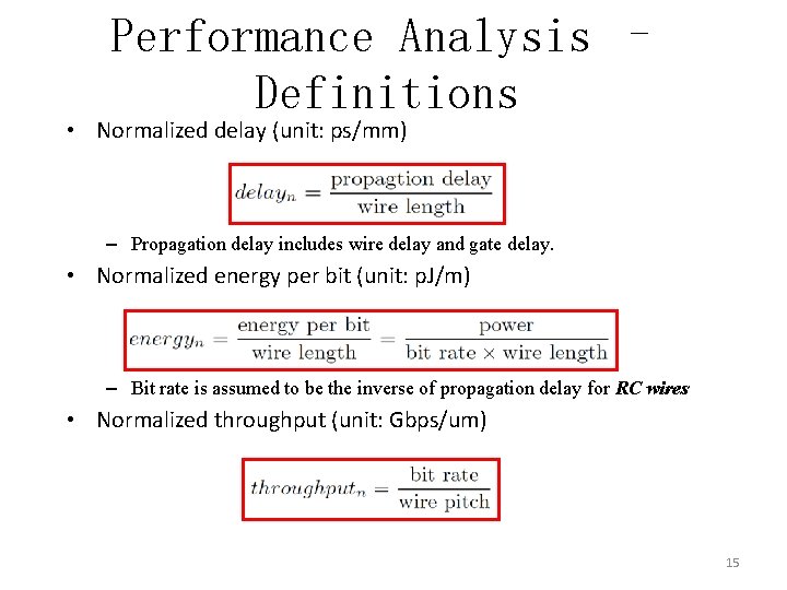
Performance Analysis – Definitions • Normalized delay (unit: ps/mm) – Propagation delay includes wire delay and gate delay. • Normalized energy per bit (unit: p. J/m) – Bit rate is assumed to be the inverse of propagation delay for RC wires • Normalized throughput (unit: Gbps/um) 15

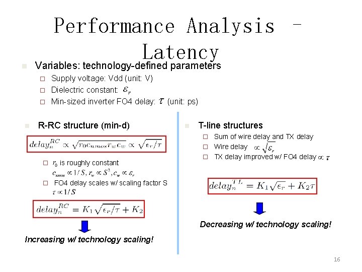
n Performance Analysis – Latency Variables: technology-defined parameters Supply voltage: Vdd (unit: V) ¨ Dielectric constant: ¨ Min-sized inverter FO 4 delay: ¨ n (unit: ps) R-RC structure (min-d) n T-line structures Sum of wire delay and TX delay ¨ Wire delay ¨ TX delay improved w/ FO 4 delay ¨ ¨ ¨ is roughly constant FO 4 delay scales w/ scaling factor S Decreasing w/ technology scaling! Increasing w/ technology scaling! 16

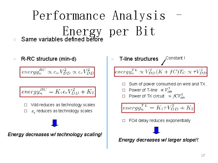
n Performance Analysis – Energy per Bit Same variables defined before n R-RC structure (min-d) n T-line structures Constant ! Sum of power consumed on wire and TX. ¨ Power of T-line ¨ Power of TX circuit ¨ Vdd reduces as technology scales ¨ ¨ Energy decreases w/ technology scaling! FO 4 delay reduces exponentially Energy decreases w/ larger slope!! 17

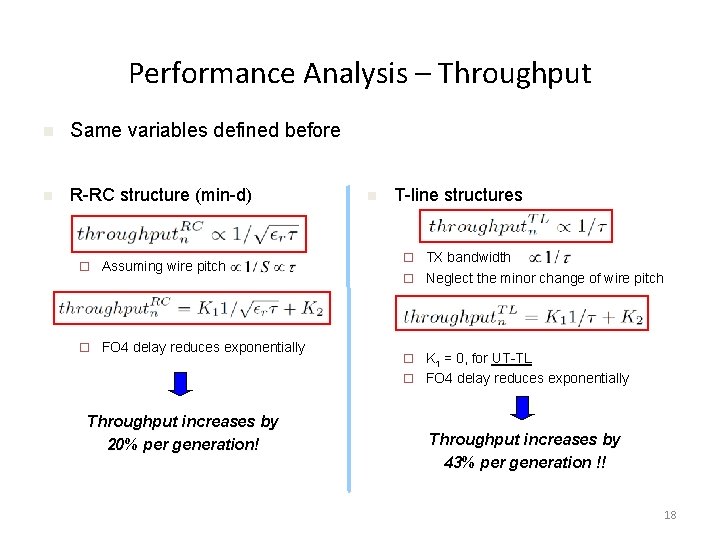
Performance Analysis – Throughput n Same variables defined before n R-RC structure (min-d) ¨ Assuming wire pitch ¨ FO 4 delay reduces exponentially Throughput increases by 20% per generation! n T-line structures TX bandwidth ¨ Neglect the minor change of wire pitch ¨ K 1 = 0, for UT-TL ¨ FO 4 delay reduces exponentially ¨ Throughput increases by 43% per generation !! 18

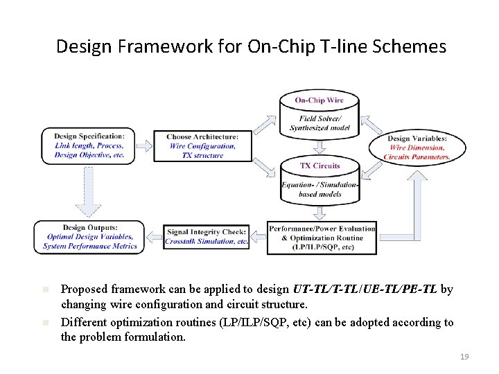
Design Framework for On-Chip T-line Schemes n n Proposed framework can be applied to design UT-TL/UE-TL/PE-TL by changing wire configuration and circuit structure. Different optimization routines (LP/ILP/SQP, etc) can be adopted according to the problem formulation. 19

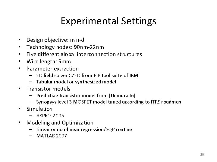
Experimental Settings • • • Design objective: min-d Technology nodes: 90 nm-22 nm Five different global interconnection structures Wire length: 5 mm Parameter extraction – 2 D field solver CZ 2 D from EIP tool suite of IBM – Tabular model or synthesized model • Transistor models – Predictive transistor model from [Uemura 06] – Synopsys level 3 MOSFET model tuned according to ITRS roadmap • Simulation – HSPICE 2005 • Modeling and Optimization – Linear or non-linear regression/SQP routine – MATLAB 2007 20

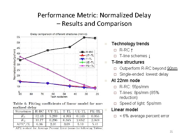
Performance Metric: Normalized Delay – Results and Comparison n Technology trends R-RC ↑ ¨ T-line schemes ↓ ¨ n T-line structures Outperform R-RC beyond 90 nm ¨ Single-ended: lowest delay ¨ n At 22 nm node R-RC: 55 ps/mm ¨ T-lines: 8 ps/mm (85% reduction) ¨ Speed of light: 5 ps/mm ¨ n Linear model ¨ < 6% average percent error 21

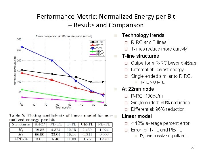
Performance Metric: Normalized Energy per Bit – Results and Comparison n Technology trends R-RC and T-lines ↓ ¨ T-lines reduce more quickly ¨ n T-line structures Outperform R-RC beyond 45 nm ¨ Differential: lowest energy. ¨ Single-ended similar to R-RC. ¨ n n T-TL > UT-TL At 22 nm node R-RC: 100 p. J/m ¨ Single-ended: 60% reduction ¨ Differential: 96% reduction ¨ n Linear model < 12% average percent error ¨ Error for T-TL and PE-TL ¨ n RL and passive equalizers. 22

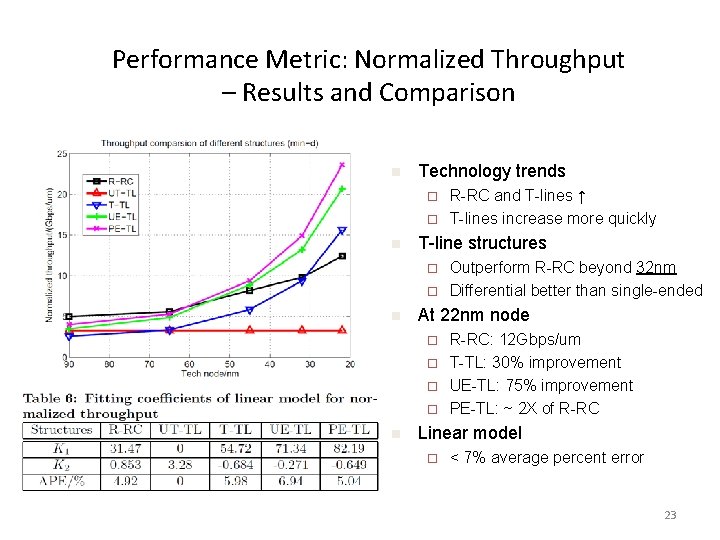
Performance Metric: Normalized Throughput – Results and Comparison n Technology trends R-RC and T-lines ↑ ¨ T-lines increase more quickly ¨ n T-line structures Outperform R-RC beyond 32 nm ¨ Differential better than single-ended ¨ n At 22 nm node R-RC: 12 Gbps/um ¨ T-TL: 30% improvement ¨ UE-TL: 75% improvement ¨ PE-TL: ~ 2 X of R-RC ¨ n Linear model ¨ < 7% average percent error 23

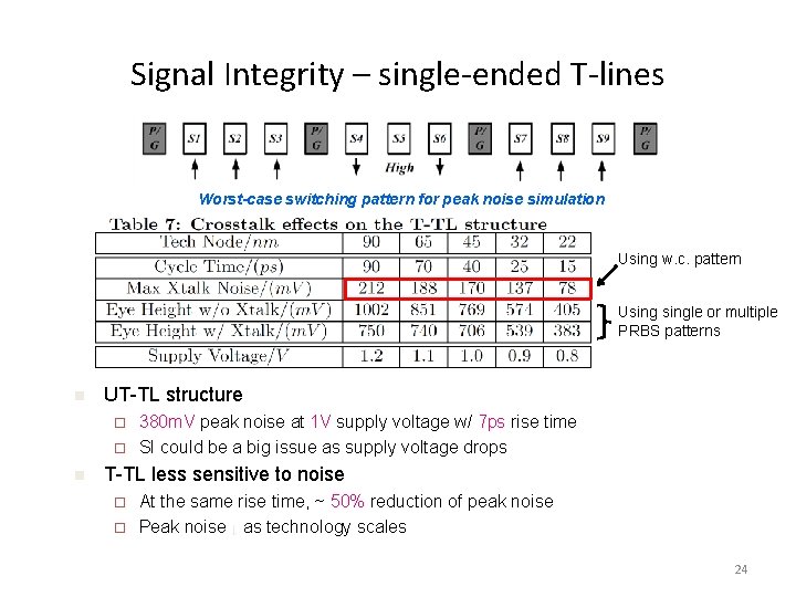
Signal Integrity – single-ended T-lines Worst-case switching pattern for peak noise simulation Using w. c. pattern Usingle or multiple PRBS patterns n UT-TL structure 380 m. V peak noise at 1 V supply voltage w/ 7 ps rise time ¨ SI could be a big issue as supply voltage drops ¨ n T-TL less sensitive to noise At the same rise time, ~ 50% reduction of peak noise ¨ Peak noise ↓ as technology scales ¨ 24

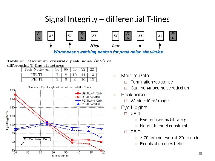
Signal Integrity – differential T-lines Worst-case switching pattern for peak noise simulation n More reliable Termination resistance ¨ Common-mode noise reduction ¨ n Peak noise ¨ n Within ~10 m. V range Eye-Heights UE-TL n Eye reduces as bit rate ↑ n Harder to meet constraint. ¨ PE-TL n > 70 m. V eye even at 22 nm node n Equalization does help! ¨ 25

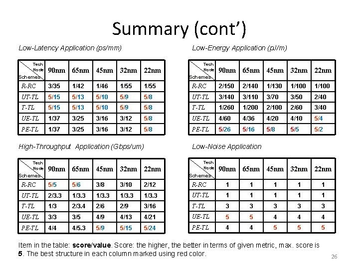
Summary (cont’) Low-Latency Application (ps/mm) Tech Node Schemes Low-Energy Application (p. J/m) 90 nm 65 nm 45 nm 32 nm 22 nm Tech Node Schemes 90 nm 65 nm 45 nm 32 nm 22 nm R-RC 3/35 1/42 1/46 1/55 R-RC 2/150 2/140 1/130 1/100 UT-TL 5/15 5/13 5/10 5/9 5/8 UT-TL 3/140 3/110 3/70 3/50 2/40 T-TL 5/15 5/13 5/10 5/9 5/8 T-TL 1/260 1/200 2/100 2/60 3/40 UE-TL 1/37 3/25 3/16 3/12 5/8 UE-TL 4/60 4/36 4/20 4/10 5/4 PE-TL 1/37 3/25 3/16 3/12 5/8 PE-TL 5/26 5/16 5/8 5/5 5/2 High-Throughput Application (Gbps/um) Tech Node Schemes Low-Noise Application 90 nm 65 nm 45 nm 32 nm 22 nm Tech Node Schemes 90 nm 65 nm 45 nm 32 nm 22 nm R-RC 5/5 5/6 3/8 3/10 2/12 R-RC 1 1 1 UT-TL 2/3. 3 1/3. 3 UT-TL 1 1 1 T-TL 1/3 2/3. 4 2/6 2/9 3/16 T-TL 3 3 3 UE-TL 3/3 3/5 4/9 4/13 4/21 UE-TL 5 5 4 4 4 PE-TL 4/4 4/5. 3 5/9 5/15 5/24 PE-TL 4 4 5 5 5 Item in the table: score/value. Score: the higher, the better in terms of given metric, max. score is 5. The best structure in each column marked using red color. 26

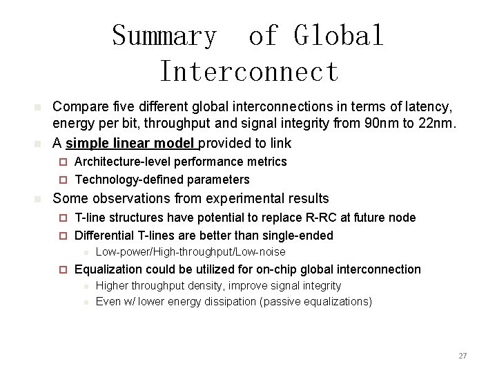
Summary of Global Interconnect n n Compare five different global interconnections in terms of latency, energy per bit, throughput and signal integrity from 90 nm to 22 nm. A simple linear model provided to link Architecture-level performance metrics ¨ Technology-defined parameters ¨ n Some observations from experimental results T-line structures have potential to replace R-RC at future node ¨ Differential T-lines are better than single-ended ¨ n ¨ Low-power/High-throughput/Low-noise Equalization could be utilized for on-chip global interconnection n n Higher throughput density, improve signal integrity Even w/ lower energy dissipation (passive equalizations) 27

Prefix Adder Synthesis • Motivation • Prefix Adder Formulation – Area/Timing/Power Models – Mixed-Radix (2, 3, 4) Adders – ILP Formulation • Experimental Results 28

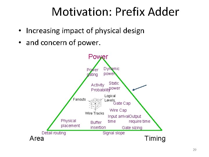
Motivation: Prefix Adder • Increasing impact of physical design • and concern of power. Power gating Dynamic power Activity Static Probabilitypower Logical Levels Fanouts Gate Cap Wire Tracks Physical placement Detail routing Area Wire Cap Input arrival. Output time require time Buffer insertion Gate sizing Signal slope Timing 29

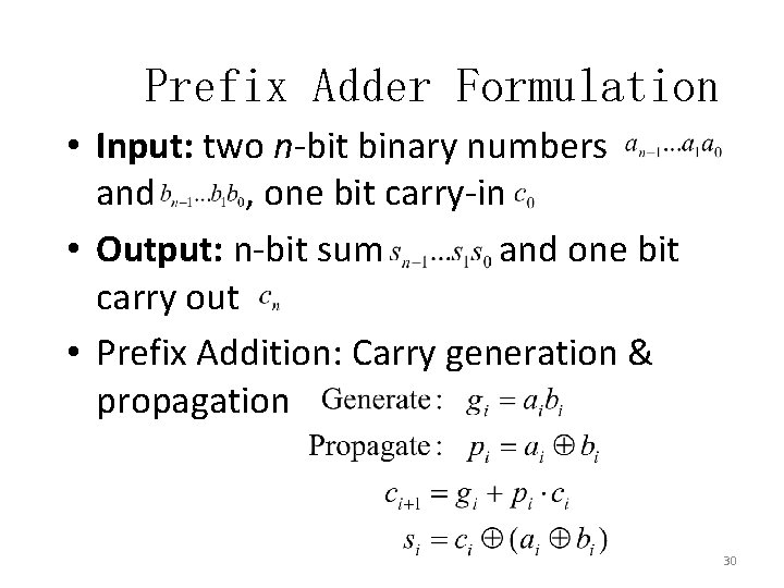
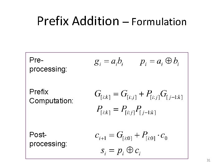
Prefix Adder Formulation • Input: two n-bit binary numbers and , one bit carry-in • Output: n-bit sum and one bit carry out • Prefix Addition: Carry generation & propagation 30

Prefix Addition – Formulation Preprocessing: Prefix Computation: Postprocessing: 31

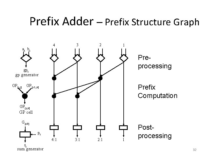
Prefix Adder – Prefix Structure Graph 4 ai bi 3 2 1 Preprocessing gpi gp generator GP[i, j] Prefix Computation GP[j-1, k] GP[i, k] GP cell G[i: 0] pi 4: 1 si sum generator 3: 1 2: 1 1 Postprocessing 32

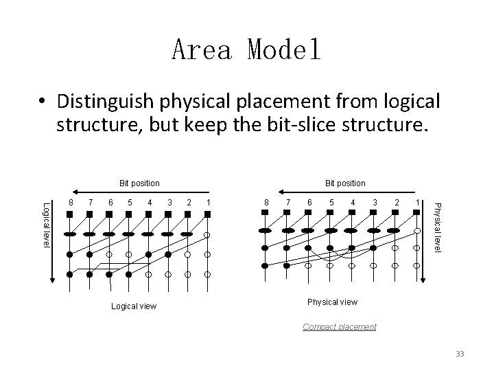
Area Model • Distinguish physical placement from logical structure, but keep the bit-slice structure. Bit position 7 6 5 4 Logical view 3 2 1 8 7 6 5 4 3 2 1 Physical level Logical level 8 Bit position Physical view Compact placement 33

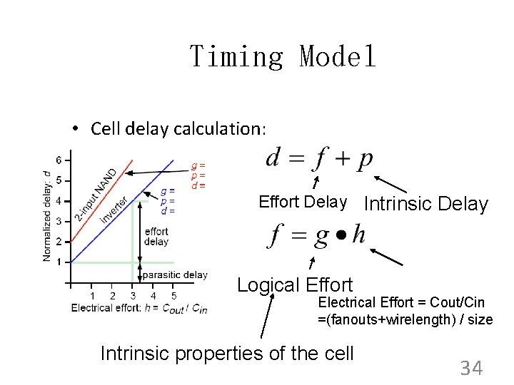
Timing Model • Cell delay calculation: Effort Delay Intrinsic Delay Logical Effort Electrical Effort = Cout/Cin =(fanouts+wirelength) / size Intrinsic properties of the cell 34

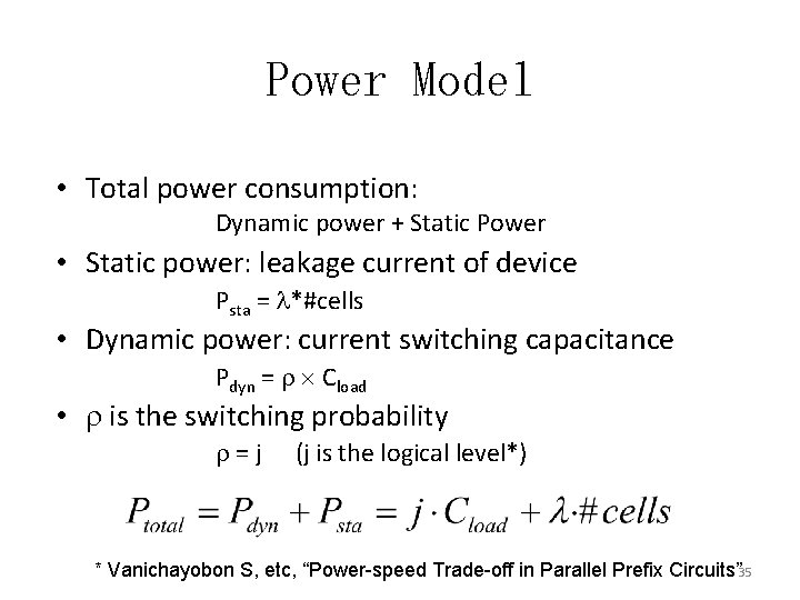
Power Model • Total power consumption: Dynamic power + Static Power • Static power: leakage current of device Psta = *#cells • Dynamic power: current switching capacitance Pdyn = Cload • is the switching probability =j (j is the logical level*) * Vanichayobon S, etc, “Power-speed Trade-off in Parallel Prefix Circuits” 35

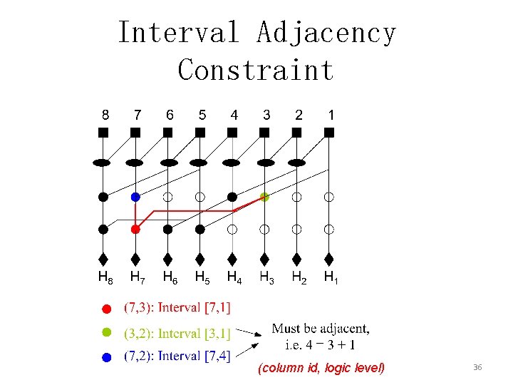
Interval Adjacency Constraint (column id, logic level) 36

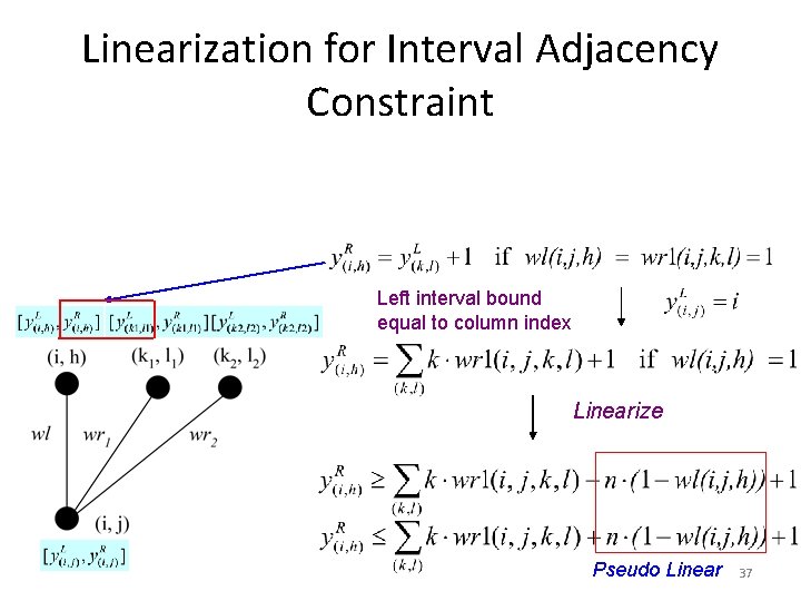
Linearization for Interval Adjacency Constraint Left interval bound equal to column index Linearize Pseudo Linear 37

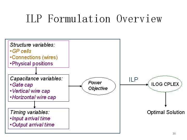
ILP Formulation Overview Structure variables: • GP cells • Connections (wires) • Physical positions Capacitance variables: • Gate cap • Vertical wire cap • Horizontal wire cap Timing variables: • Input arrival time • Output arrival time Power Objective ILP ILOG CPLEX Optimal Solution 38

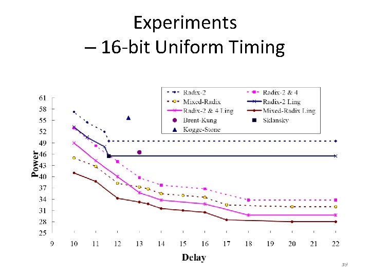
Experiments – 16 -bit Uniform Timing 39

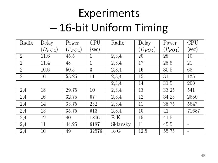
Experiments – 16 -bit Uniform Timing 40

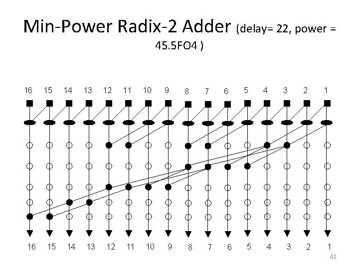
Min-Power Radix-2 Adder (delay= 22, power = 45. 5 FO 4 ) 16 16 15 15 14 14 13 13 12 12 11 11 10 10 9 9 8 8 7 7 6 6 5 5 4 4 3 3 2 2 1 1 41

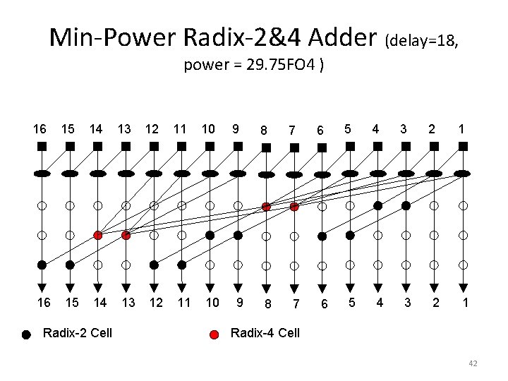
Min-Power Radix-2&4 Adder (delay=18, power = 29. 75 FO 4 ) 16 16 15 15 14 14 Radix-2 Cell 13 13 12 12 11 11 10 10 9 9 8 8 7 7 6 6 5 5 4 4 3 3 2 2 1 1 Radix-4 Cell 42

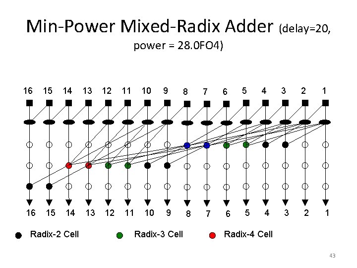
Min-Power Mixed-Radix Adder (delay=20, power = 28. 0 FO 4) 16 16 15 15 14 14 Radix-2 Cell 13 13 12 12 11 10 9 9 Radix-3 Cell 8 8 7 7 6 6 5 5 4 4 3 3 2 2 1 1 Radix-4 Cell 43

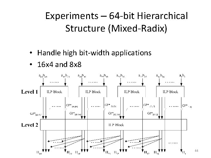
Experiments – 64 -bit Hierarchical Structure (Mixed-Radix) • Handle high bit-width applications • 16 x 4 and 8 x 8 44

FPGA Global Routing Architecture • Synthesis Flow • Formulation • Experimental Results 45

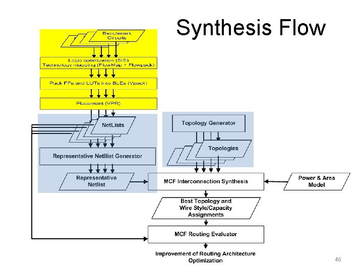
Synthesis Flow 46

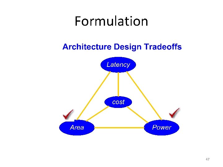
Formulation 47

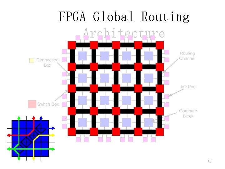
FPGA Global Routing Architecture 48

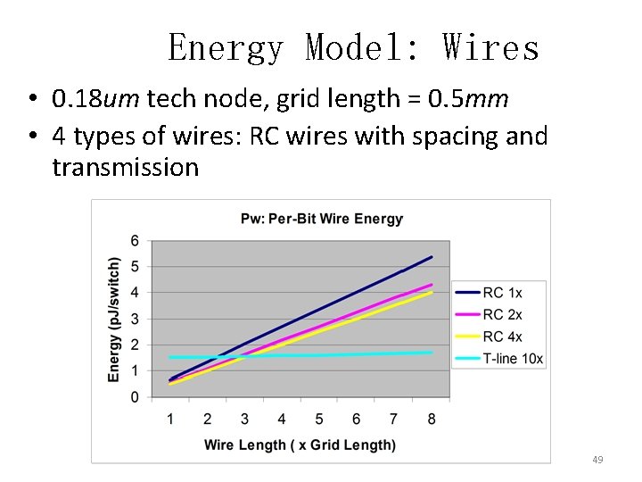
Energy Model: Wires • 0. 18 um tech node, grid length = 0. 5 mm • 4 types of wires: RC wires with spacing and transmission 49

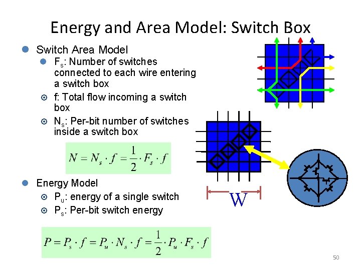
Energy and Area Model: Switch Box l Switch Area Model l Fs: Number of switches connected to each wire entering a switch box ¤ f: Total flow incoming a switch box ¤ Ns: Per-bit number of switches inside a switch box l Energy Model ¤ Pu: energy of a single switch ¤ Ps: Per-bit switch energy W 50

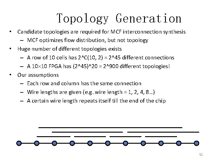
Topology Generation • Candidate topologies are required for MCF interconnection synthesis – MCF optimizes flow distribution, but not topology • Huge number of different topologies exists – A row of 10 cells has 2^C(10, 2) = 2^45 different connections – A 10 10 FPGA has (2^45)^20 = 2^900 different topologies! • Our assumptions – Each row and column has the same connection – Wire lengths are given (e. g. wire length = 1, 2, 4, 8…) – A certain wire length repeats itself till the end of the chip 51

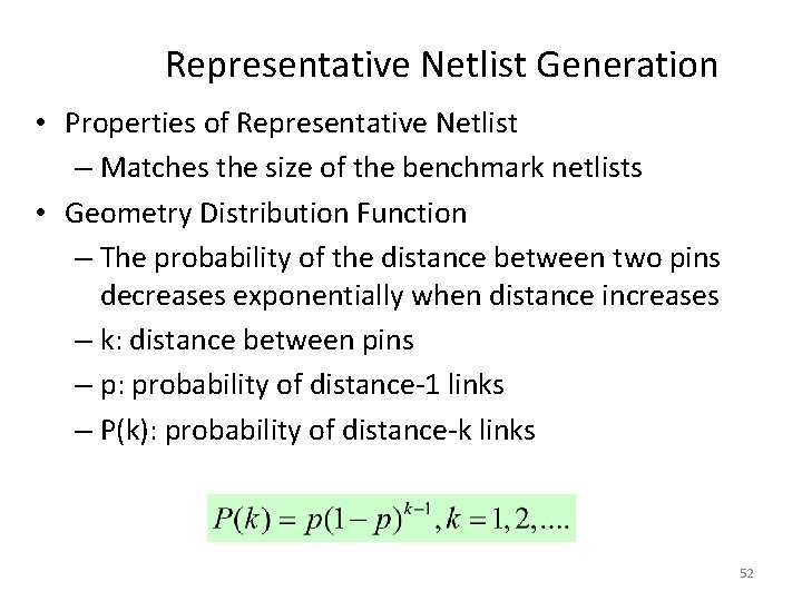
Representative Netlist Generation • Properties of Representative Netlist – Matches the size of the benchmark netlists • Geometry Distribution Function – The probability of the distance between two pins decreases exponentially when distance increases – k: distance between pins – p: probability of distance-1 links – P(k): probability of distance-k links 52

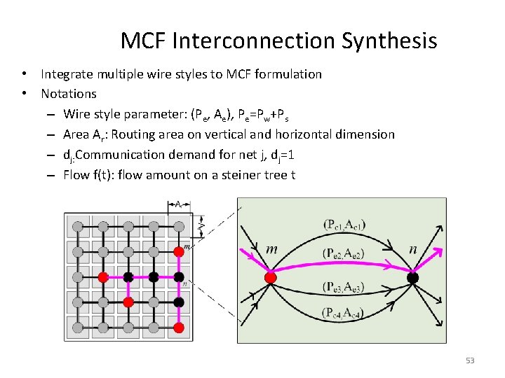
MCF Interconnection Synthesis • Integrate multiple wire styles to MCF formulation • Notations – Wire style parameter: (Pe, Ae), Pe=Pw+Ps – Area Ar: Routing area on vertical and horizontal dimension – dj: Communication demand for net j, dj=1 – Flow f(t): flow amount on a steiner tree t 53

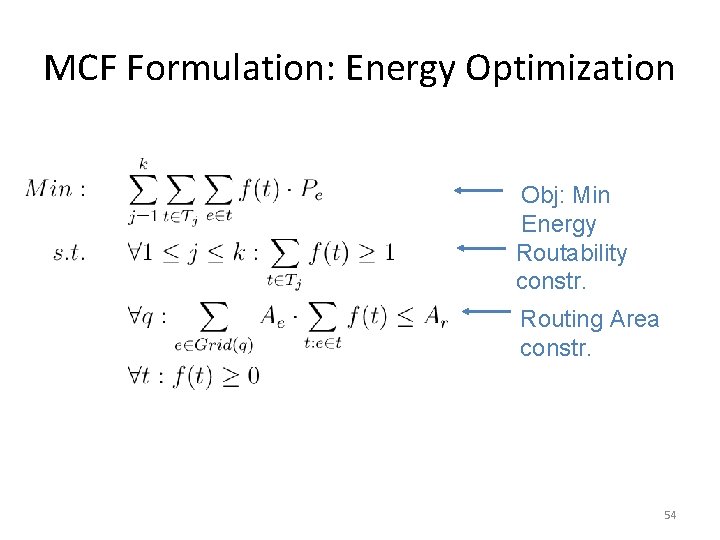
MCF Formulation: Energy Optimization Obj: Min Energy Routability constr. Routing Area constr. 54

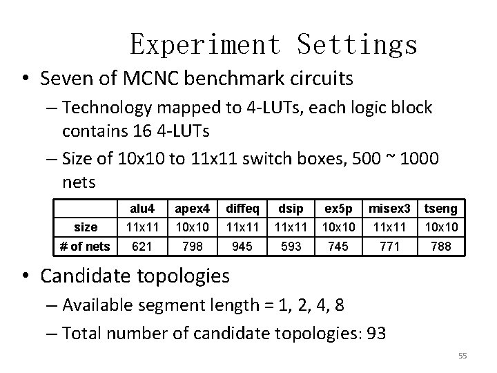
Experiment Settings • Seven of MCNC benchmark circuits – Technology mapped to 4 -LUTs, each logic block contains 16 4 -LUTs – Size of 10 x 10 to 11 x 11 switch boxes, 500 ~ 1000 nets alu 4 apex 4 diffeq dsip ex 5 p misex 3 tseng size 11 x 11 10 x 10 # of nets 621 798 945 593 745 771 788 • Candidate topologies – Available segment length = 1, 2, 4, 8 – Total number of candidate topologies: 93 55

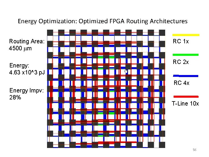
Energy Optimization: Optimized FPGA Routing Architectures Routing Area: 1500 m 2500 3500 4500 Energy: 6. 46 x 10^3 p. J 5. 24 4. 74 4. 63 RC 1 x RC 2 x RC 4 x Energy Impv: 19% 27% 28% T-Line 10 x 56

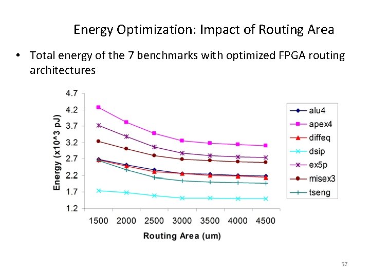
Energy Optimization: Impact of Routing Area • Total energy of the 7 benchmarks with optimized FPGA routing architectures 57

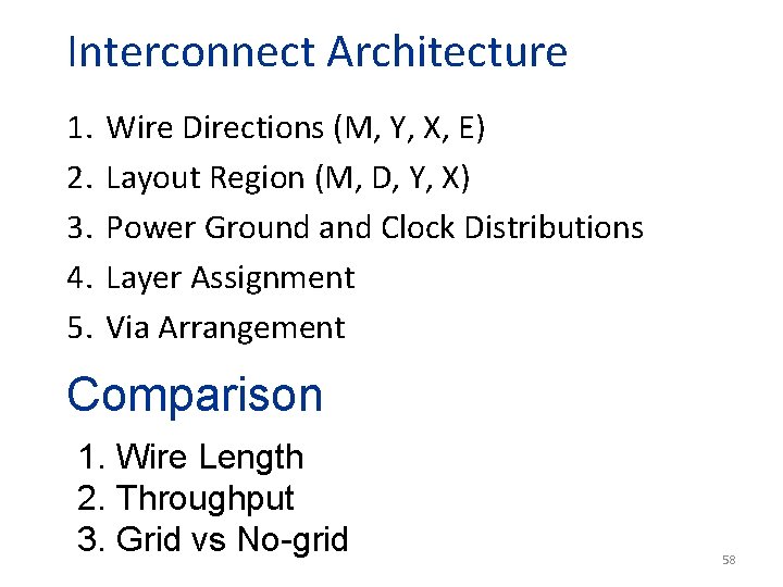
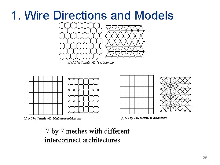
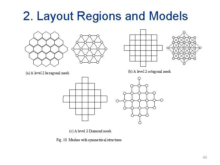
Interconnect Architecture 1. 2. 3. 4. 5. Wire Directions (M, Y, X, E) Layout Region (M, D, Y, X) Power Ground and Clock Distributions Layer Assignment Via Arrangement Comparison 1. Wire Length 2. Throughput 3. Grid vs No-grid 58

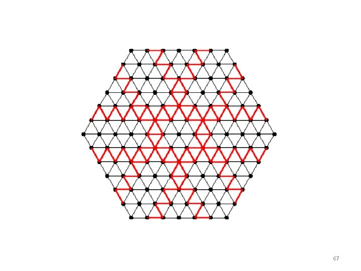
1. Wire Directions and Models (a) A 7 by 7 mesh with Y-architecture (b) A 7 by 7 mesh with Manhattan-architecture (c) A 7 by 7 mesh with X-architecture 7 by 7 meshes with different interconnect architectures 59

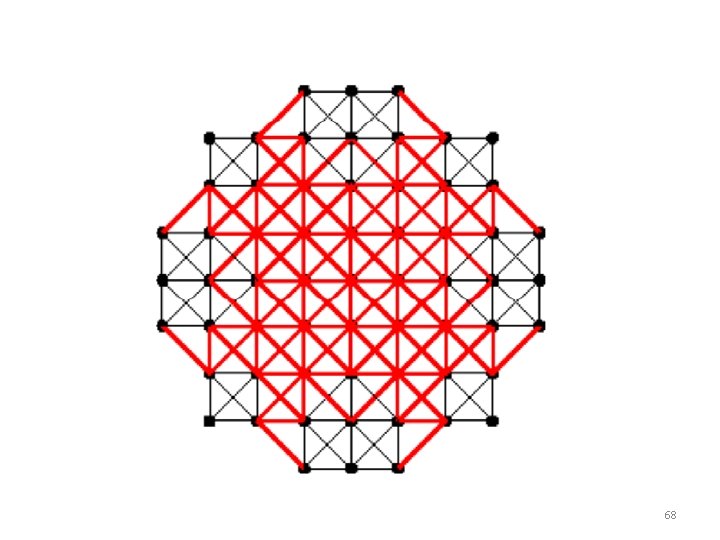
2. Layout Regions and Models (b) A level 2 octagonal mesh (a) A level 2 hexagonal mesh (c) A level 2 Diamond mesh Fig. 10 Meshes with symmetrical structures 60

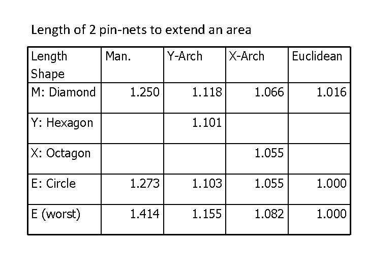
Length of 2 pin-nets to extend an area Length Man. Y-Arch X-Arch Euclidean Shape M: Diamond 1. 250 1. 118 1. 066 1. 016 Y: Hexagon 1. 101 X: Octagon 1. 055 E: Circle 1. 273 1. 103 1. 055 1. 000 E (worst) 1. 414 1. 155 1. 082 1. 000

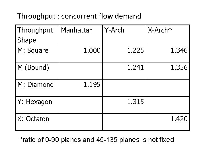
Throughput : concurrent flow demand Throughput Shape M: Square Manhattan 1. 000 M (Bound) M: Diamond Y: Hexagon X: Octafon Y-Arch X-Arch* 1. 225 1. 346 1. 241 1. 356 1. 195 1. 315 1. 420 *ratio of 0 -90 planes and 45 -135 planes is not fixed

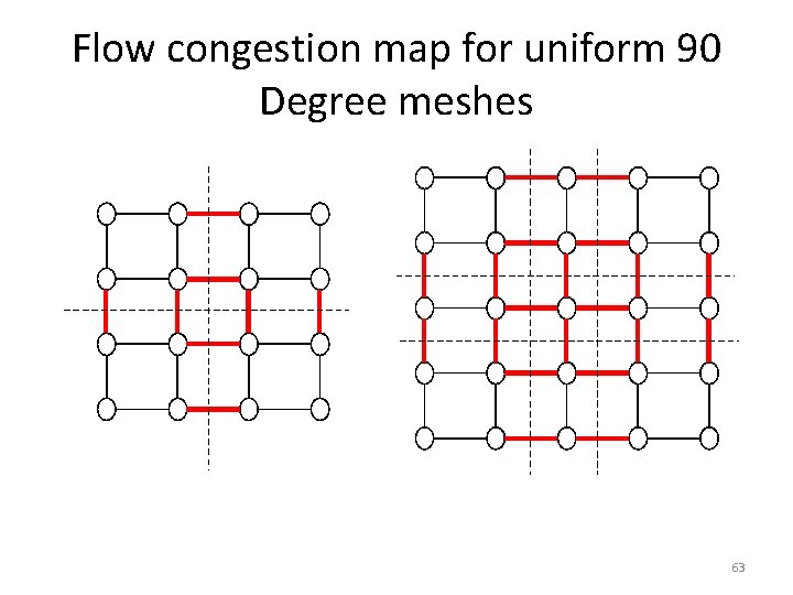
Flow congestion map for uniform 90 Degree meshes 63

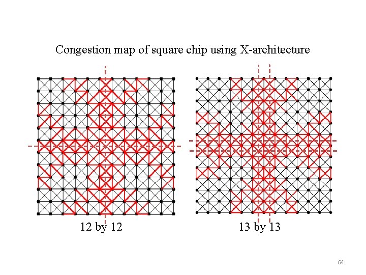
Congestion map of square chip using X-architecture 12 by 12 13 by 13 64

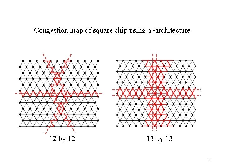
Congestion map of square chip using Y-architecture 12 by 12 13 by 13 65

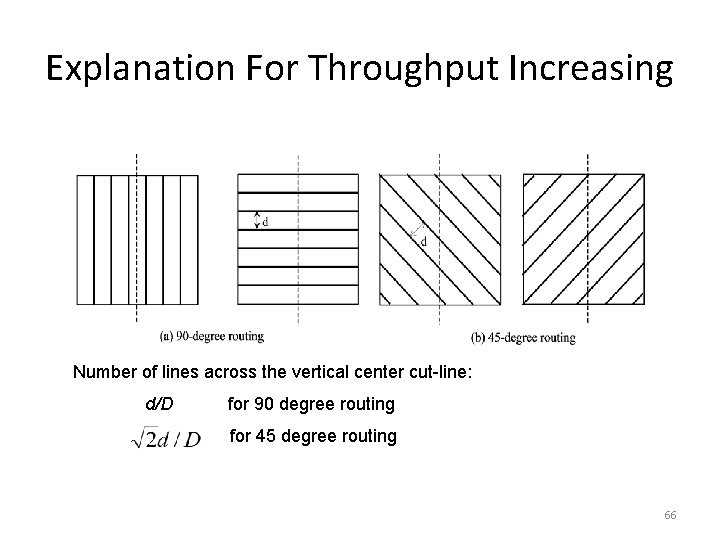
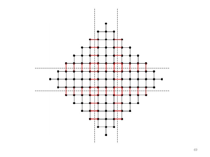
Explanation For Throughput Increasing Number of lines across the vertical center cut-line: d/D for 90 degree routing for 45 degree routing 66

67

68

69

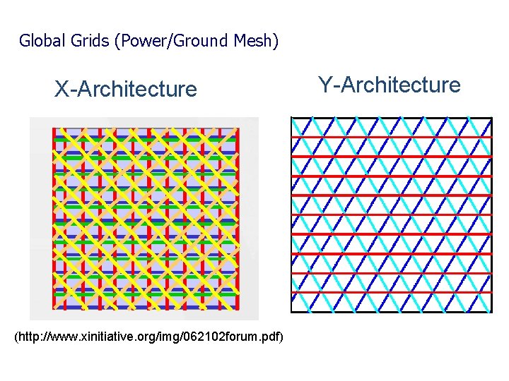
Global Grids (Power/Ground Mesh) X-Architecture (http: //www. xinitiative. org/img/062102 forum. pdf) Y-Architecture

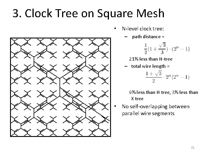
3. Clock Tree on Square Mesh • N-level clock tree: – path distance = 21% less than H-tree – total wire length = 9% less than H tree, 3% less than X tree • No self-overlapping between parallel wire segments 71

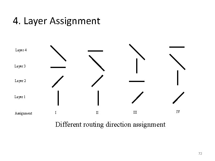
4. Layer Assignment Layer 4 Layer 3 Layer 2 Layer 1 Assignment I II IV Different routing direction assignment 72

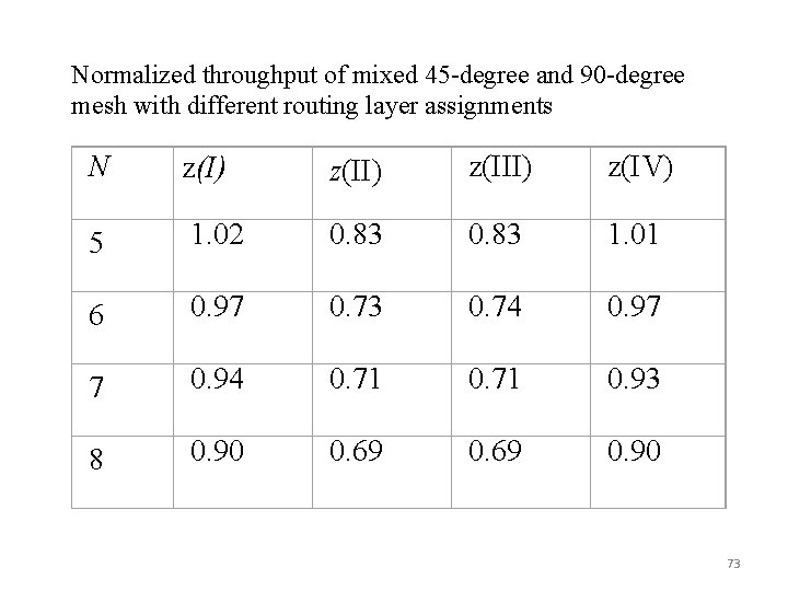
Normalized throughput of mixed 45 -degree and 90 -degree mesh with different routing layer assignments N z(I) z(III) z(IV) 5 1. 02 0. 83 1. 01 6 0. 97 0. 73 0. 74 0. 97 7 0. 94 0. 71 0. 93 8 0. 90 0. 69 0. 90 73

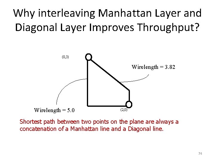
Why interleaving Manhattan Layer and Diagonal Layer Improves Throughput? (0, 3) Wirelength = 3. 82 Wirelength = 5. 0 (2, 0) Shortest path between two points on the plane are always a concatenation of a Manhattan line and a Diagonal line. 74

Observations • Routing Direction Assignment Strategies Can Affect the Communication Throughput. • Interleaving the Manhattan Routing Layers and Diagonal Routing Layers can produce better Throughput 75

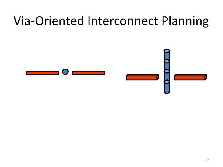
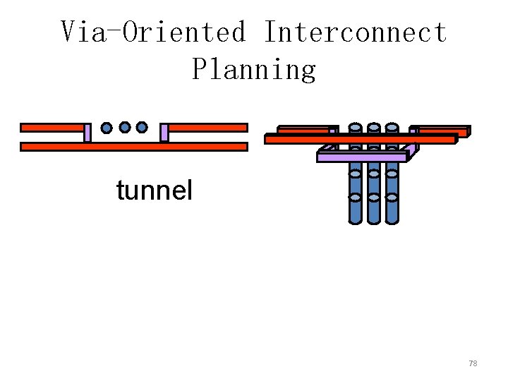
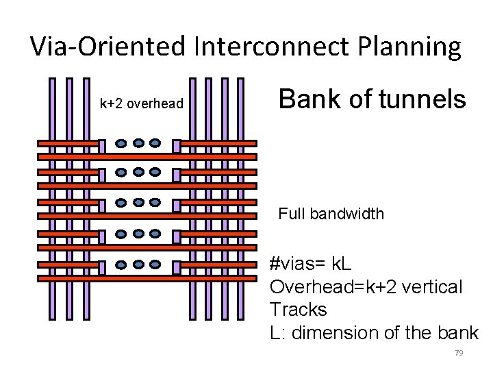
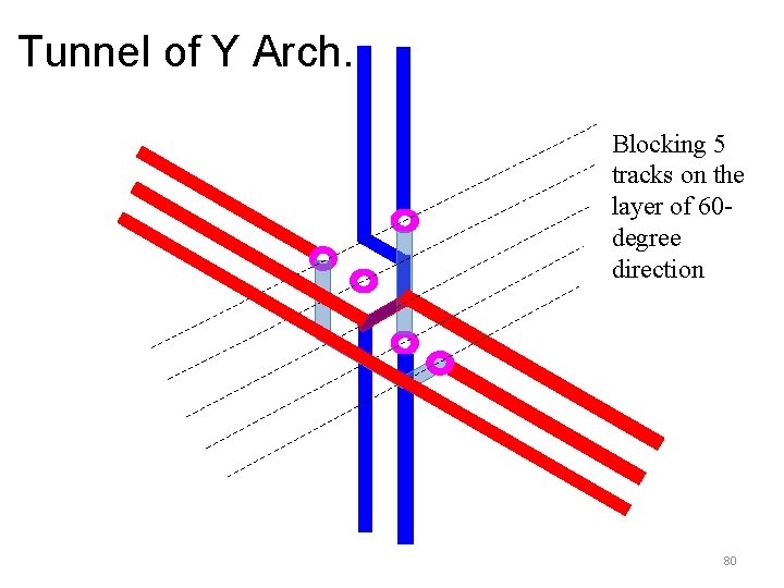
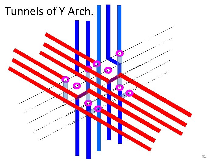
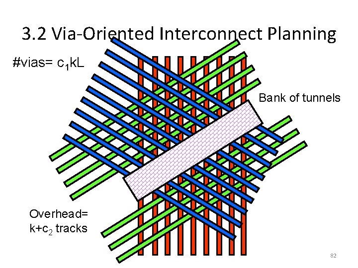
5. Via Arrangement: Banks and Tunnels • Use tunnels to detour around vias • Use banks of tunnels to maximize throughput • Use bottom k layers to perform intracell routing • Use top n-k layers to distribute signals to the banks 76

Via-Oriented Interconnect Planning 77

Via-Oriented Interconnect Planning tunnel 78

Via-Oriented Interconnect Planning k+2 overhead Bank of tunnels Full bandwidth #vias= k. L Overhead=k+2 vertical Tracks L: dimension of the bank 79

Tunnel of Y Arch. Blocking 5 tracks on the layer of 60 degree direction 80

Tunnels of Y Arch. 81

3. 2 Via-Oriented Interconnect Planning #vias= c 1 k. L Bank of tunnels Overhead= k+c 2 tracks 82

Conclusion • Global Interconnect Technologies – EM waves + Devices • Prefix Adder Synthesis – Formulation + ILP • FPGA Interconnect Architecture – Formulation + LP • Interconnect Architecture – Lambda Geometry + Vias 83

Thank you! Q&A 84