
Wires wire delay Lecture 9 Tuesday September 27
Wires & wire delay Lecture 9 Tuesday September 27, 2016
Outline • Introduction • Interconnect Modeling – Wire Resistance – Wire Capacitance • Introducing a distributed wire RC p-model • Estimating wire RC delay assuming a dominant time constant • Elmore delay model – a generalized model • Handling wire branches • Inserting repeaters to keep wire lengths short September 2016 Introduction to Integrated Circuit Design 2
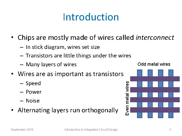
Introduction • Chips are mostly made of wires called interconnect – In stick diagram, wires set size – Transistors are little things under the wires – Many layers of wires Odd metal wires – Speed – Power – Noise • Alternating layers run orthogonally September 2016 Introduction to Integrated Circuit Design Even metal wires • Wires are as important as transistors 3
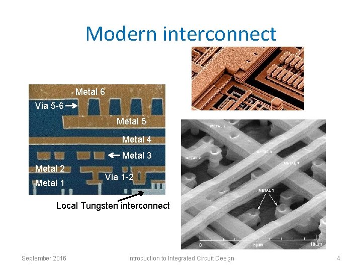
Modern interconnect Metal 6 Via 5 -6 Metal 5 Metal 4 Metal 3 Metal 2 Metal 1 Via 1 -2 Local Tungsten interconnect September 2016 Introduction to Integrated Circuit Design 4
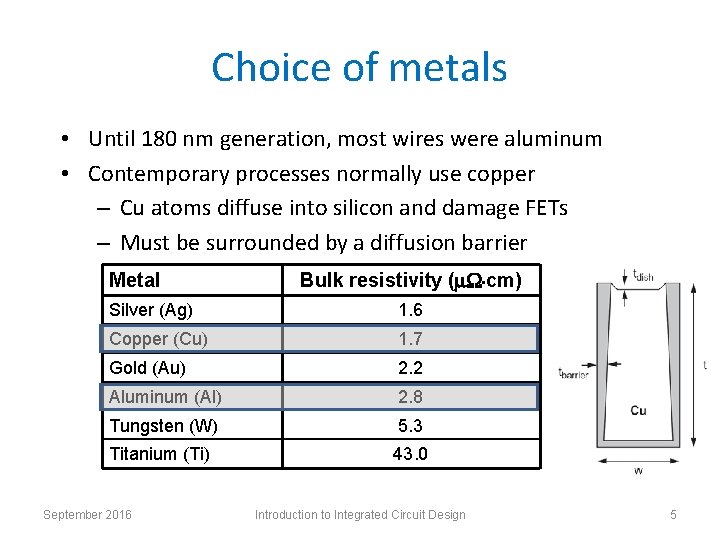
Choice of metals • Until 180 nm generation, most wires were aluminum • Contemporary processes normally use copper – Cu atoms diffuse into silicon and damage FETs – Must be surrounded by a diffusion barrier Metal Bulk resistivity (m. W • cm) Silver (Ag) 1. 6 Copper (Cu) 1. 7 Gold (Au) 2. 2 Aluminum (Al) 2. 8 Tungsten (W) 5. 3 Titanium (Ti) 43. 0 September 2016 Introduction to Integrated Circuit Design 5
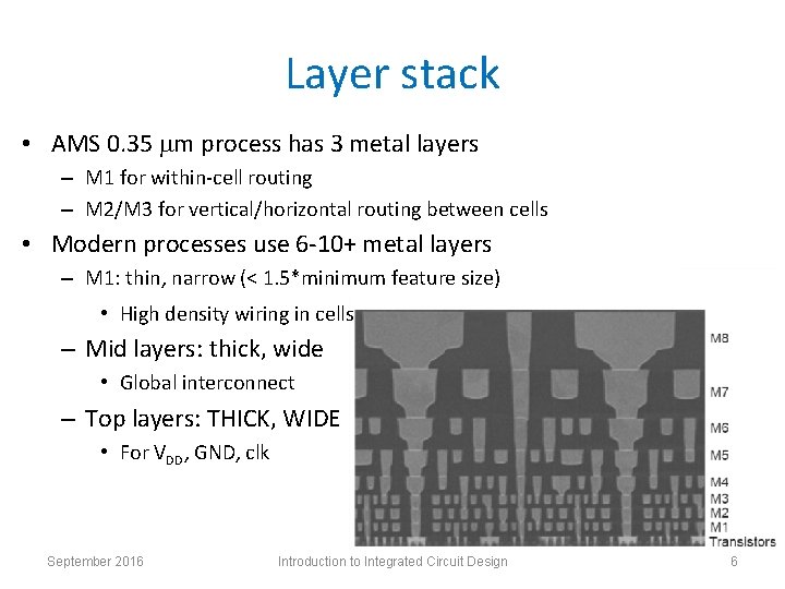
Layer stack • AMS 0. 35 mm process has 3 metal layers – M 1 for within-cell routing – M 2/M 3 for vertical/horizontal routing between cells • Modern processes use 6 -10+ metal layers – M 1: thin, narrow (< 1. 5*minimum feature size) • High density wiring in cells – Mid layers: thick, wide • Global interconnect – Top layers: THICK, WIDE • For VDD, GND, clk September 2016 Introduction to Integrated Circuit Design 6
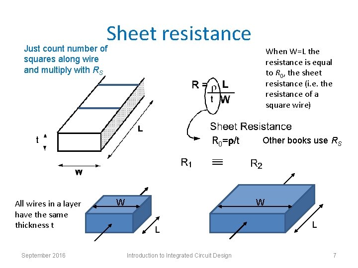
Sheet resistance Just count number of squares along wire and multiply with RS When W=L the resistance is equal to R 0, the sheet resistance (i. e. the resistance of a square wire) t t All wires in a layer have the same thickness t September 2016 R 0=r/t W Other books use RS W L Introduction to Integrated Circuit Design L 7
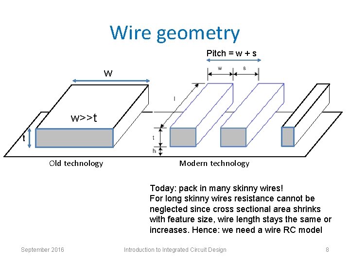
Wire geometry Pitch = w + s w w>>t t Old technology Modern technology Today: pack in many skinny wires! For long skinny wires resistance cannot be neglected since cross sectional area shrinks with feature size, wire length stays the same or increases. Hence: we need a wire RC model September 2016 Introduction to Integrated Circuit Design 8
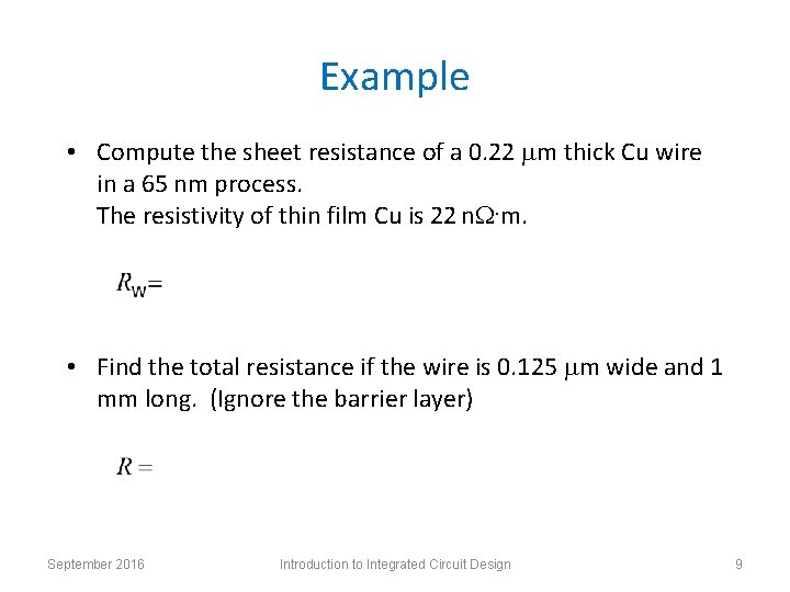
Example • Compute the sheet resistance of a 0. 22 mm thick Cu wire in a 65 nm process. The resistivity of thin film Cu is 22 n. W. m. • Find the total resistance if the wire is 0. 125 mm wide and 1 mm long. (Ignore the barrier layer) September 2016 Introduction to Integrated Circuit Design 9
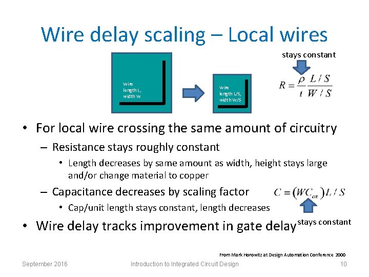
Wire delay scaling – Local wires stays constant Wire length L, width W Wire length L/S, width W/S • For local wire crossing the same amount of circuitry – Resistance stays roughly constant • Length decreases by same amount as width, height stays large and/or change material to copper – Capacitance decreases by scaling factor • Cap/unit length stays constant, length decreases • Wire delay tracks improvement in gate delay stays constant From Mark Horowitz at Design Automation Conference 2000 September 2016 Introduction to Integrated Circuit Design 10
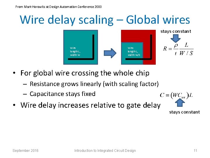
From Mark Horowitz at Design Automation Conference 2000 Wire delay scaling – Global wires stays constant Wire length L, width W/S • For global wire crossing the whole chip – Resistance grows linearly (with scaling factor) – Capacitance stays fixed • Wire delay increases relative to gate delay September 2016 Introduction to Integrated Circuit Design stays constant 11
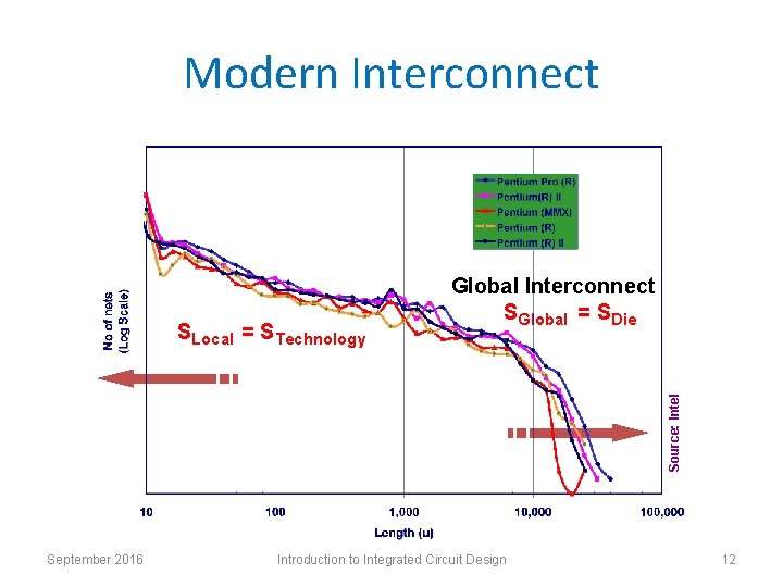
Modern Interconnect Source: Intel SLocal = STechnology Global Interconnect SGlobal = SDie September 2016 Introduction to Integrated Circuit Design 12
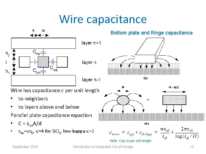
Wire capacitance Bottom plate and fringe capacitance Wire has capacitance c per unit length • to neighbors • to layers above and below Parallel plate capacitance equation • C = eox. A/d • eox=ke 0, k≈4 for Si. O 2, low-kappa k<3 Note: Cap is per unit length September 2016 Introduction to Integrated Circuit Design 13
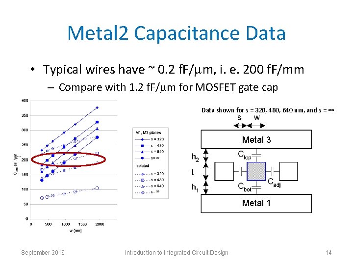
Metal 2 Capacitance Data • Typical wires have ~ 0. 2 f. F/mm, i. e. 200 f. F/mm – Compare with 1. 2 f. F/mm for MOSFET gate cap Data shown for s = 320, 480, 640 nm, and s = ∞ Metal 3 Metal 1 September 2016 Introduction to Integrated Circuit Design 14
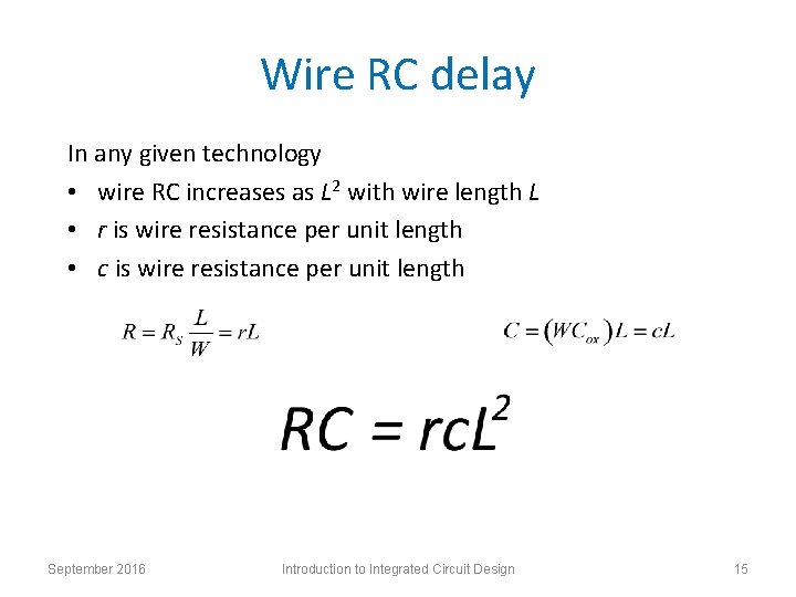
Wire RC delay In any given technology • wire RC increases as L 2 with wire length L • r is wire resistance per unit length • c is wire resistance per unit length September 2016 Introduction to Integrated Circuit Design 15
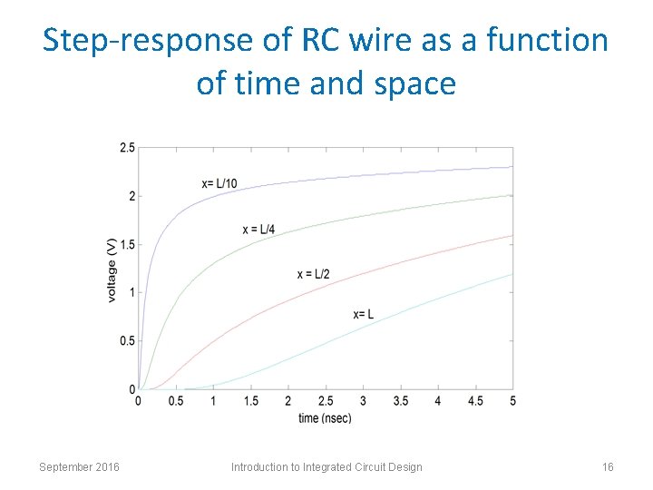
Step-response of RC wire as a function of time and space September 2016 Introduction to Integrated Circuit Design 16
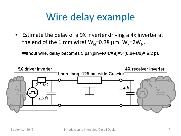
Wire delay example • Estimate the delay of a 9 X inverter driving a 4 x inverter at the end of the 1 mm wire! WN=0. 78 mm. WP=2 WN. Assume c=becomes 200 f. F/mm, r=800 W/mm from previous example Without wire, cap delay 5 ps*(pinv+X 4/X 9)=5*(0. 8+4/9)= 6. 2 ps 9 X driver inverter 9 X CG 1 mm long, 125 nm wide Cu wire 4 X receiver inverter 4 X 2. 2 k. W 1. 4 f. F Reff CD 2. 6 f. F September 2016 Introduction to Integrated Circuit Design 17
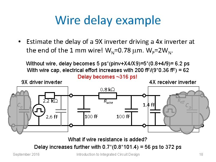
Wire delay example • Estimate the delay of a 9 X inverter driving a 4 x inverter at the end of the 1 mm wire! WN=0. 78 mm. WP=2 WN. Without wire, delay becomes 5 ps*(pinv+X 4/X 9)=5*(0. 8+4/9)= 6. 2 ps With wire cap, electrical effort increases with 200 f. F/(9*0. 36 f. F) = 62 Delay becomes ~316 ps! 9 X driver inverter 4 X receiver inverter 0. 8 k. W 9 X 4 X Reff Rwire 2. 2 k. W 1. 4 f. F CG CD 2. 6 f. F 100 f. F What if wire resistance is added? Delay increases further with 0. 7*(0. 8*101. 4) = 56 ps to 372 ps September 2016 Introduction to Integrated Circuit Design 18
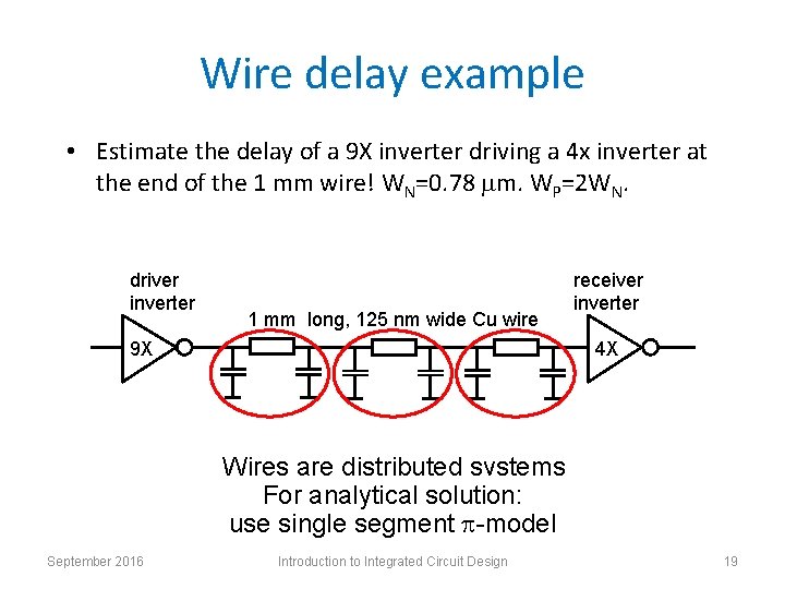
Wire delay example • Estimate the delay of a 9 X inverter driving a 4 x inverter at the end of the 1 mm wire! WN=0. 78 mm. WP=2 WN. driver inverter 1 mm long, 125 nm wide Cu wire 9 X receiver inverter 4 X Wires are distributed systems For with analytical solution: Approximate lumped element models use single segment p-model In Spice simulations a 3 -segment p-model is accurate to 3% September 2016 Introduction to Integrated Circuit Design 19
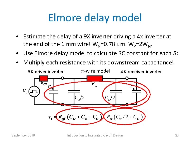
Elmore delay model • Estimate the delay of a 9 X inverter driving a 4 x inverter at the end of the 1 mm wire! WN=0. 78 mm. WP=2 WN. • Use Elmore delay model to calculate RC constant for each R: • Multiply each resistance with its downstream capacitance! 9 X driver inverter Reff V 0 September 2016 p-wire model 4 X receiver inverter Rw CD Cw/2 CG Cw/2 Introduction to Integrated Circuit Design 20
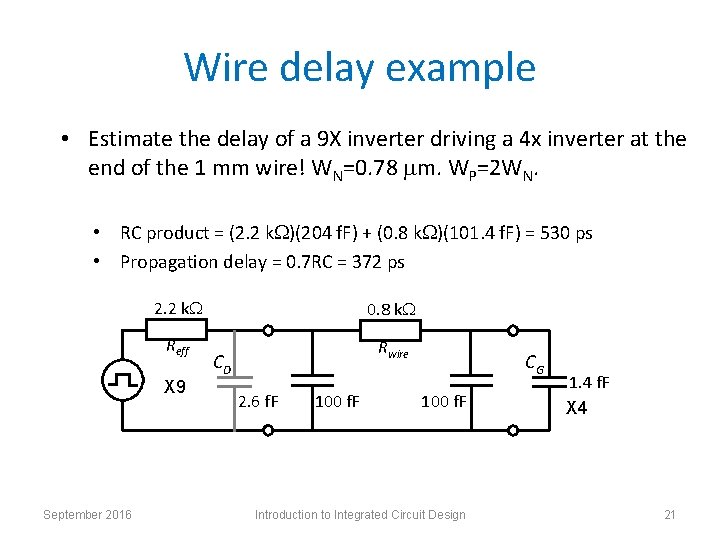
Wire delay example • Estimate the delay of a 9 X inverter driving a 4 x inverter at the end of the 1 mm wire! WN=0. 78 mm. WP=2 WN. • RC product = (2. 2 k. W)(204 f. F) + (0. 8 k. W)(101. 4 f. F) = 530 ps • Propagation delay = 0. 7 RC = 372 ps 2. 2 k. W 0. 8 k. W Reff Rwire X 9 September 2016 CD 2. 6 f. F 100 f. F CG 100 f. F Introduction to Integrated Circuit Design 1. 4 f. F X 4 21
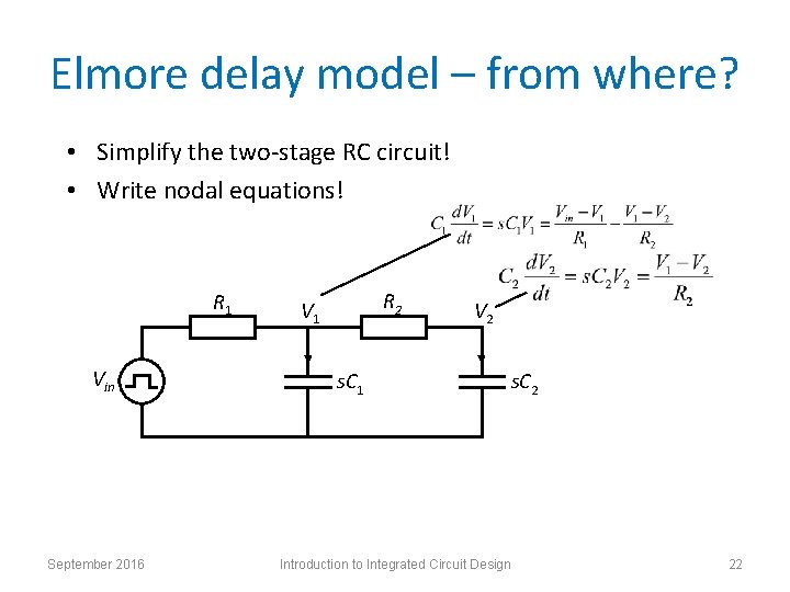
Elmore delay model – from where? • Simplify the two-stage RC circuit! • Write nodal equations! R 1 Vin September 2016 R 2 V 1 s. C 1 V 2 s. C 2 Introduction to Integrated Circuit Design 22
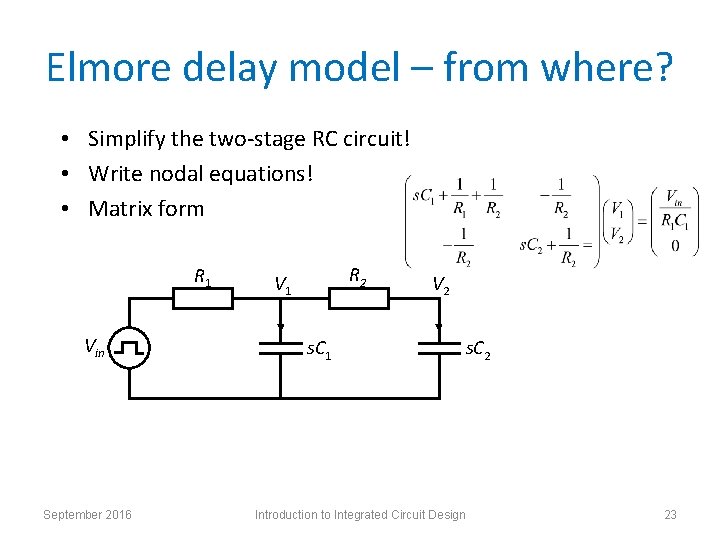
Elmore delay model – from where? • Simplify the two-stage RC circuit! • Write nodal equations! • Matrix form R 1 Vin September 2016 R 2 V 1 s. C 1 V 2 s. C 2 Introduction to Integrated Circuit Design 23
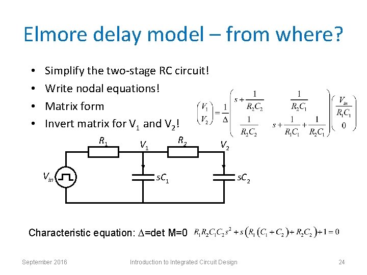
Elmore delay model – from where? • • Simplify the two-stage RC circuit! Write nodal equations! Matrix form Invert matrix for V 1 and V 2! R 1 Vin R 2 V 1 s. C 1 V 2 s. C 2 Characteristic equation: D=det M=0 September 2016 Introduction to Integrated Circuit Design 24
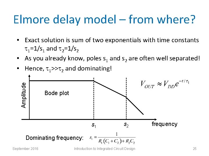
Elmore delay model – from where? Amplitude • Exact solution is sum of two exponentials with time constants t 1=1/s 1 and t 2=1/s 2 • As you already know, poles s 1 and s 2 are often well separated! • Hence, t 1>>t 2 and dominating! Bode plot s 1 s 2 frequency Dominating frequency: September 2016 Introduction to Integrated Circuit Design 25
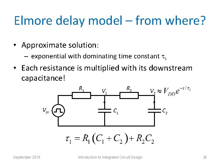
Elmore delay model – from where? • Approximate solution: – exponential with dominating time constant t 1 • Each resistance is multiplied with its downstream capacitance! R 1 Vin September 2016 R 2 V 1 C 1 Introduction to Integrated Circuit Design V 2 C 2 26
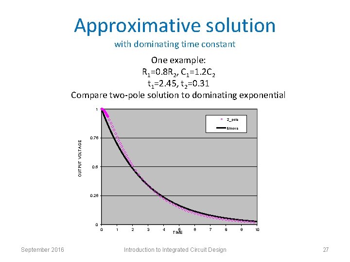
Approximative solution with dominating time constant One example: R 1=0. 8 R 2, C 1=1. 2 C 2 t 1=2. 45, t 2=0. 31 Compare two-pole solution to dominating exponential 1 2_pole OUTPUT VOLTAGE Elmore 0. 75 0. 25 0 0 September 2016 1 2 3 4 5 TIME 6 7 8 Introduction to Integrated Circuit Design 9 10 27
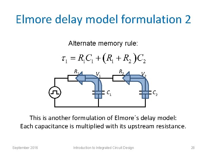
Elmore delay model formulation 2 Alternate memory rule: R 1 R 2 V 1 C 1 V 2 C 2 This is another formulation of Elmore´s delay model: Each capacitance is multiplied with its upstream resistance. September 2016 Introduction to Integrated Circuit Design 28
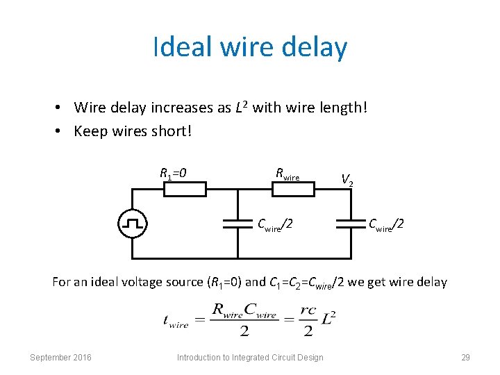
Ideal wire delay • Wire delay increases as L 2 with wire length! • Keep wires short! R 1=0 Rwire Cwire/2 V 2 Cwire/2 Most often(Rt 11=0) >>tand dominating! For an ideal voltage source C 1=C 2 and 2=Cwire/2 we get wire delay September 2016 Introduction to Integrated Circuit Design 29
Summary • We have introduced a wire p-RC model • We have analytically solved for delayed output response • We simplified using dominant time constant • We arrived at Elmore´s wire delay model! September 2016 Introduction to Integrated Circuit Design 30
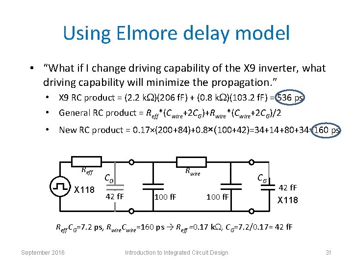
Using Elmore delay model • “What if I change driving capability of the X 9 inverter, what driving capability will minimize the propagation. ” • X 9 RC product = (2. 2 k. W)(206 f. F) + (0. 8 k. W)(103. 2 f. F) = 536 ps • General RC product = Reff*(Cwire+2 CG)+Rwire*(Cwire+2 CG)/2 • New RC product = 0. 17×(200+84)+0. 8×(100+42)=34+14+80+34≈160 ps Has minimum when Reff*Cwire=Rwire*CG, i. e. for 2. 2 k. W 0. 17 k. W Reff X 118 X 9 0. 8 k. W Rwire CD 42 f. F 3. 2 100 f. F CG 100 f. F slightly changed capacitance values 42 f. F 3. 2 f. F X 9 X 118 Reff CG=7. 2 ps, Rwire. Cwire=160 ps → Reff =0. 17 k. W, CG=7. 2/0. 17= 42 f. F September 2016 Introduction to Integrated Circuit Design 31
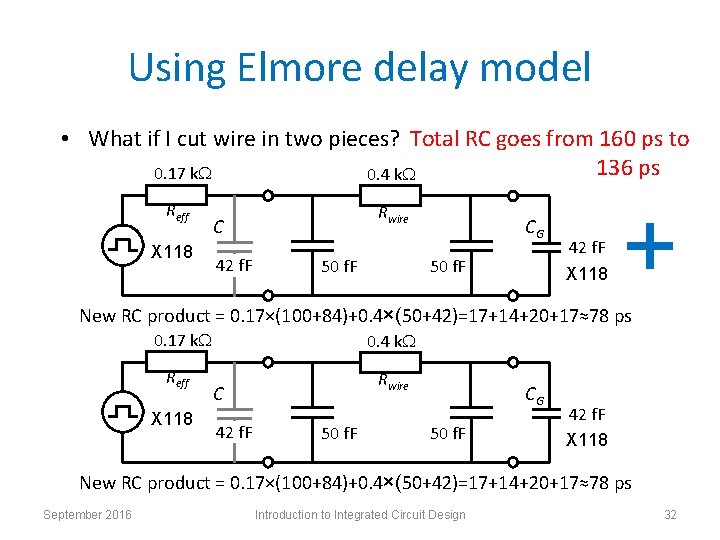
Using Elmore delay model • What if I cut wire in two pieces? Total RC goes from 160 ps to 136 ps 0. 17 k. W 0. 4 k. W Reff X 118 Rwire C 42 f. F CG 50 f. F 42 f. F X 118 + New RC product = 0. 17×(100+84)+0. 4×(50+42)=17+14+20+17≈78 ps 0. 17 k. W Reff X 118 0. 4 k. W Rwire C 42 f. F 50 f. F CG 50 f. F 42 f. F X 118 New RC product = 0. 17×(100+84)+0. 4×(50+42)=17+14+20+17≈78 ps September 2016 Introduction to Integrated Circuit Design 32
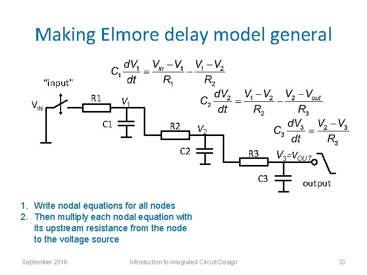
Making Elmore delay model general “input" VIN R 1 V 1 C 1 R 2 V 2 C 2 R 3 C 3 V 3=VOUT output 1. Write nodal equations for all nodes 2. Then multiply each nodal equation with its upstream resistance from the node to the voltage source September 2016 Introduction to Integrated Circuit Design 33
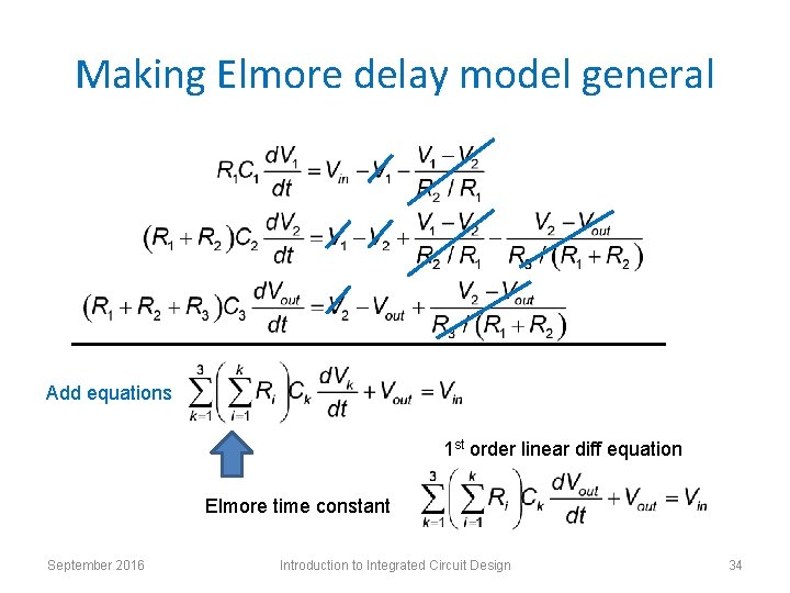
Making Elmore delay model general Add equations 1 st order linear diff equation Elmore time constant September 2016 Introduction to Integrated Circuit Design 34
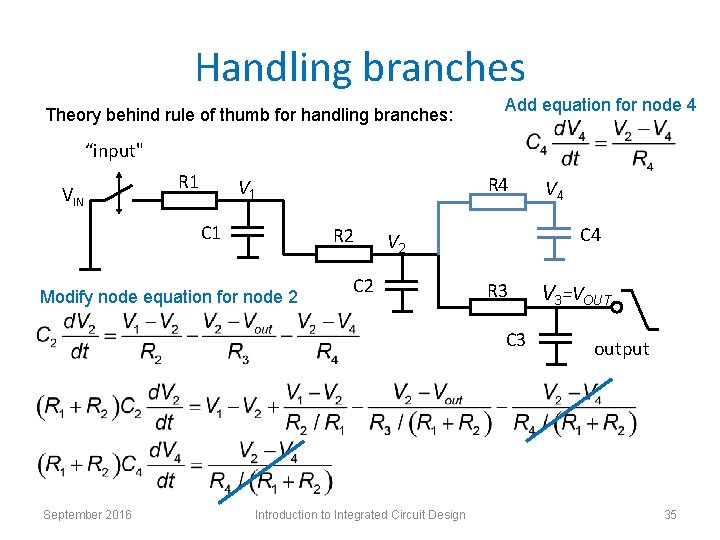
Handling branches Theory behind rule of thumb for handling branches: Add equation for node 4 “input" VIN R 1 R 4 V 1 C 1 R 2 Modify node equation for node 2 C 4 V 2 C 2 R 3 C 3 September 2016 Introduction to Integrated Circuit Design V 4 V 3=VOUT output 35
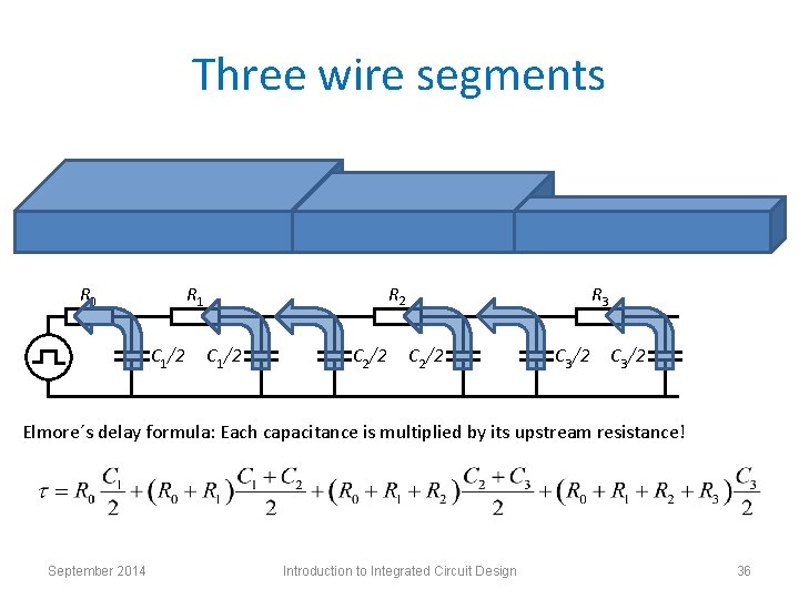
Three wire segments R 0 R 2 R 1 C 1/2 C 2/2 R 3 C 2/2 C 3/2 Elmore´s delay formula: Each capacitance is multiplied by its upstream resistance! September 2014 Introduction to Integrated Circuit Design 36
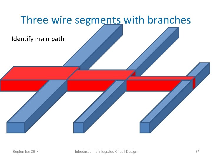
Three wire segments with branches Identify main path September 2014 Introduction to Integrated Circuit Design 37
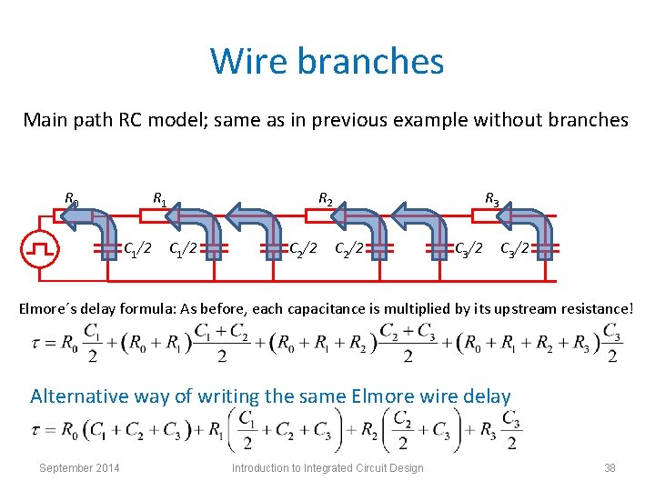
Wire branches Main path RC model; same as in previous example without branches R 0 R 2 R 1 C 1/2 C 2/2 R 3 C 2/2 C 3/2 Elmore´s delay formula: As before, each capacitance is multiplied by its upstream resistance! Alternative way of writing the same Elmore wire delay September 2014 Introduction to Integrated Circuit Design 38
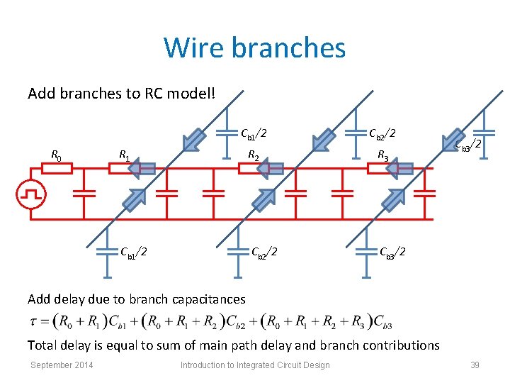
Wire branches Add branches to RC model! R 0 Cb 1/2 Cb 2/2 R 1 R 2 R 3 Cb 1/2 Cb 2/2 Cb 3/2 Add delay due to branch capacitances Total delay is equal to sum of main path delay and branch contributions September 2014 Introduction to Integrated Circuit Design 39

Driving long wires with repeaters • Since wire delay increases as L 2 with wire length, it could be advantageous to divide long wires into segments driven by repeaters Repeater data: input and output cap Crep, effective resistance Rrep Rw/m Cw/2 m Rw/m Cw/2 m Determine delay ofthe m number segments ofcan segments be written that minimizes The number of increase linearly as m, but delay: the delay of each wire • There is a critical wire length when repeaters should be considered segment decreases as 1/m 2 September 2014 Introduction to Integrated Circuit Design 40
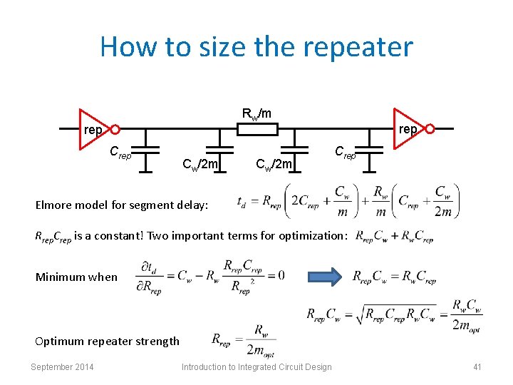
How to size the repeater Rw/m rep Cw/2 m rep Crep Elmore model for segment delay: Rrep. Crep is a constant! Two important terms for optimization: Minimum when Optimum repeater strength September 2014 Introduction to Integrated Circuit Design 41
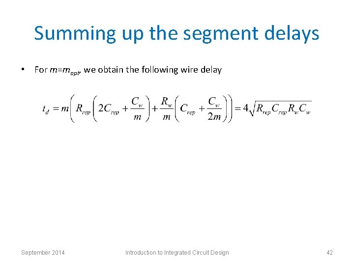
Summing up the segment delays • For m=mopt, we obtain the following wire delay September 2014 Introduction to Integrated Circuit Design 42
Conclusion • Importance of wire delay • Introduced distributed wire RC p-model • Discussed relevance of delay equations using a dominant time constant model • Using delay model to minimize wire delay • Elmore delay model – a generalized model • Mathematics behind Elmore model • Handling branches • Repeater insertion September 2016 Introduction to Integrated Circuit Design 43
- Slides: 43