Development of CVD Diamond Tracking Detectors for Experiments
- Slides: 41

Development of CVD Diamond Tracking Detectors for Experiments at High Luminosity Colliders RD 42 Status Report Peter Weilhammer CERN and Ohio State University for the RD 42 Collaboration LHCC Presentation CERN, February 18, 2010 1

RD 42 Collaboration 2010 M. Artuso 25, D. Asner 22, M. Barbero 1, V. Bellini 2, V. Belyaev 15, E. Berdermann 8, P. Bergonzo 14, S. Blusk 25, A. Borgia 25, J-M. Brom 10, M. Bruzzi 5, D. Chren 23, V. Cindro 12, G. Claus 10, M. Cristinziani 1, S. Costa 2, J. Cumalat 24, R. D’Alessandro 6, W. de Boer 13, D. Dobos 3, I. Dolenc 12, W. Dulinski 10, J. Duris 20, V. Eremin 9, R. Eusebi 7, H. Frais-Kolbl 4, A. Furgeri 13, K. K. Gan 16, M. Goffe 10, J. Goldstein 21, A. Golubev 11, A. Gorisek 12, E. Griesmayer 4, E. Grigoriev 11, D. Hits 17, M. Hoeferkamp 26, F. Huegging 1, H. Kagan 16, t, R. Kass 16, G. Kramberger 12, S. Kuleshov 11, S. Kwan 7, S. Lagomarsino 6, A. La Rosa 3, A. Lo Giudice 18, I. Mandic 12, C. Manfredotti 18, A. Martemyanov 11, D. Menichelli 5, M. Mikuz 12, M. Mishina 7, J. Moss 16, R. Mountain 25, S. Mueller 13, G. Oakham 22, A. Oh 27, P. Olivero 18, G. Parrini 6, H. Pernegger 3, M. Pomorski 14, R. Potenza 2, K. Randrianarivony 22, A. Robichaud 22, S. Roe 3, S. Schnetzer 17, T. Schreiner 4, S. Sciortino 6, S. Seidel 26, S. Smith 16, B. Sopko 23, K. Stenson 24, R. Stone 17, C. Sutera 2, M. Traeger 8, D. Tromson 14, W. Trischuk 19, J-W. Tsung 1, C. Tuve 2, P. Urquijo 25, J. Velthuis 21, E. Vittone 18, S. Wagner 24, J. Wang 25, R. Wallny 20, P. Weilhammer 3, t, N. Wermes 1 t Spokespersons 1 Universitat at Bonn, Germany 2 INFN/University of Catania, Italy 3 CERN, Geneva, Switzerland 4 Wiener Neustadt, Austria 5 INFN/University of Florence, Italy 6 Department of Energetics/INFN, Florence, Italy 7 FNAL, Batavia, USA 8 GSI, Darmstadt, Germany 9 Ioffe Institute, St. Petersburg, Russia 10 IPHC, Strasbourg, France 11 ITEP, Moscow, Russia 12 Jozef Stefan Institute, Ljubljana, Slovenia 13 Universitat at Karlsruhe, Germany 14 CEA-LIST, Saclay, France 15 MEPHI Institute, Moscow, Russia 16 Ohio State University, Columbus, OH, USA 17 Rutgers University, Piscataway, NJ, USA 18 University of Torino, Italy 19 University of Toronto, ON, Canada 20 UCLA, Los Angeles, CA, USA 21 University of Bristol, UK 22 Carleton University, Ottawa, Canada 23 Czech Technical Univ. , Prague, Czech Republic 24 University of Colorado, Boulder, CO, USA 25 Syracuse University, Syracuse, NY, USA 26 University of New Mexico, Albuquerque, NM, USA 27 University of Manchester, UK 70 g 87 Participants February 18, 2010 P. Weilhammer – RD 42 LHCC Report 22 g 27 Institutes 2

Outline of Talk Ø Ø Ø Ø February 18, 2010 Introduction Material and manufacturers Radiation Hardness Studies Pixel Module Construction and Results Applications in Experiments Requests from CERN Summary P. Weilhammer – RD 42 LHCC Report 3

INTRODUCTION Motivation: Need Tracking Devices Close to Interaction Region of Experiments at LHC and more important at s. LHC Possible Materials with adequate properties: ► Radiation Hardness (possibly survive to end of experiment) ► Low dielectric constant low capacitance ► Low leakage current (even after strong irradiation) low noise for readout ► Room temperature operation ► Fast signal collection Many materials are and have been considered: Clearly Silicon: but radiation hardness of Si at 1016 p/cm 2 is also difficult, Was p on, now n on p? 4 H-Si. C, 6 H-Si. C, Ga. N, Ga. As, CZT, a-Si(H), … CVD diamond will be discussed in this talk February 18, 2010 P. Weilhammer – RD 42 LHCC Report 4

INTRODUCTION Main activities in RD 42: ► Material Studies ► Radiation Hardness tests of presently highest quality p. CVD and sc. CVD diamond ► Beam tests to characterize quality ► Pixel module preparation and tests ► Manufacturing Developments ► So far diamond material supplied by/in collaboration with Diamond Detector Ltd/ Element Six Ltd. ► See also: http: //rd 42. web. cern. ch/RD 42 February 18, 2010 P. Weilhammer – RD 42 LHCC Report 5

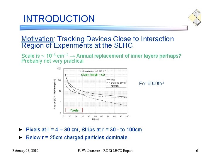
O INTRODUCTION Motivation: Tracking Devices Close to Interaction Region of Experiments at the SLHC Scale is ~ 1016 cm− 2 → Annual replacement of inner layers perhaps? Probably not very practical For 6000 fb-1 ► Pixels at r = 4 – 30 cm, Strips at r = 30 - to 100 cm ► Below r = 25 cm charged particles dominate February 18, 2010 P. Weilhammer – RD 42 LHCC Report 6

Material and Manufacturers Polycrystalline CVD Diamond (p. CVD) First measurements on new samples done with 90 Sr sources: ► Contacts on both sides- contact structures from several mm to cm ► Usually operate at 1 – 2 V/mm ► Test procedure: dot strips pixels on same diamond February 18, 2010 P. Weilhammer – RD 42 LHCC Report 7

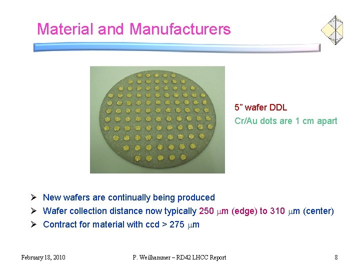
Material and Manufacturers 5” wafer DDL Cr/Au dots are 1 cm apart Ø New wafers are continually being produced Ø Wafer collection distance now typically 250 mm (edge) to 310 mm (center) Ø Contract for material with ccd > 275 mm February 18, 2010 P. Weilhammer – RD 42 LHCC Report 8

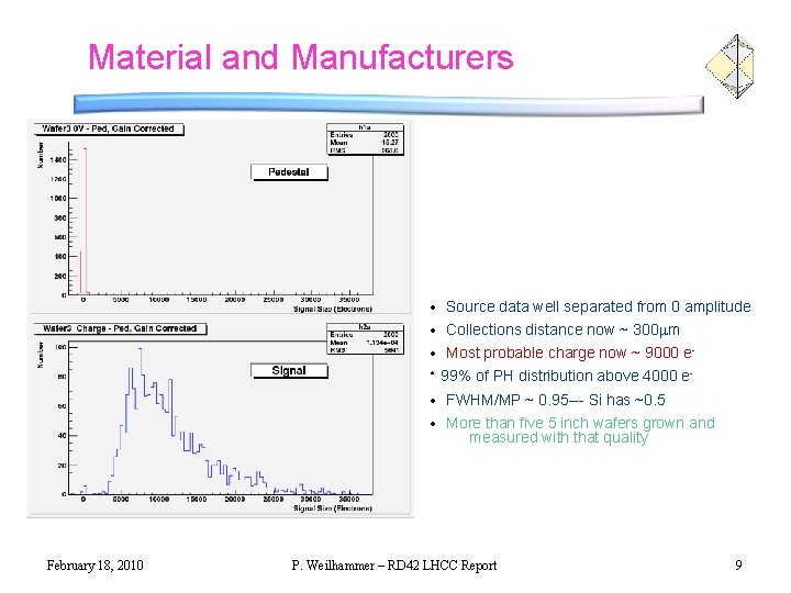
Material and Manufacturers • Source data well separated from 0 amplitude • Collections distance now ~ 300 mm • Most probable charge now ~ 9000 e • 99% of PH distribution above 4000 e • FWHM/MP ~ 0. 95 --- Si has ~0. 5 • More than five 5 inch wafers grown and measured with that quality February 18, 2010 P. Weilhammer – RD 42 LHCC Report 9

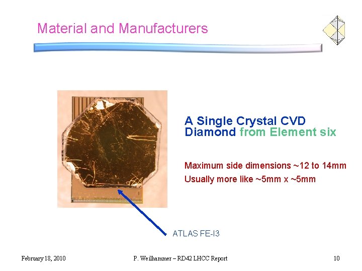
Material and Manufacturers A Single Crystal CVD Diamond from Element six Maximum side dimensions ~12 to 14 mm Usually more like ~5 mm x ~5 mm ATLAS FE-I 3 February 18, 2010 P. Weilhammer – RD 42 LHCC Report 10

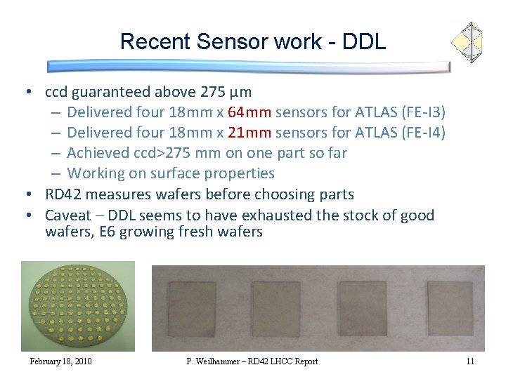
Recent Sensor work - DDL • ccd guaranteed above 275 µm – Delivered four 18 mm x 64 mm sensors for ATLAS (FE-I 3) – Delivered four 18 mm x 21 mm sensors for ATLAS (FE-I 4) – Achieved ccd>275 mm on one part so far – Working on surface properties • RD 42 measures wafers before choosing parts • Caveat – DDL seems to have exhausted the stock of good wafers, E 6 growing fresh wafers February 18, 2010 P. Weilhammer – RD 42 LHCC Report 11

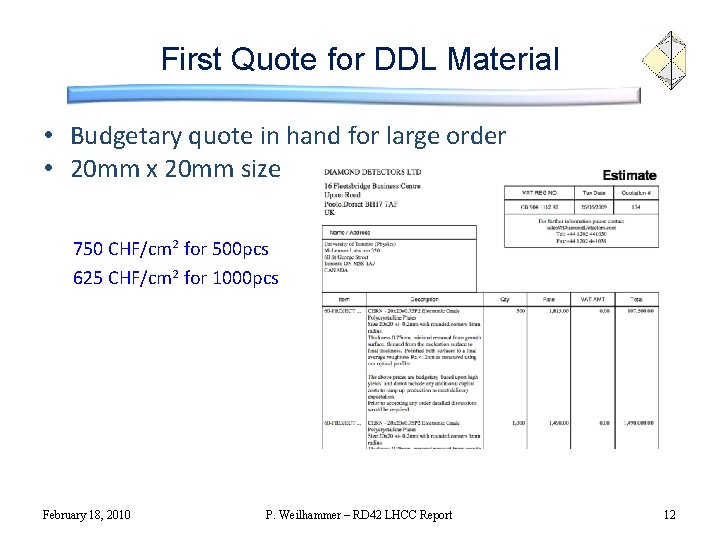
First Quote for DDL Material • Budgetary quote in hand for large order • 20 mm x 20 mm size 750 CHF/cm 2 for 500 pcs 625 CHF/cm 2 for 1000 pcs February 18, 2010 P. Weilhammer – RD 42 LHCC Report 12

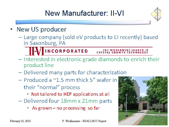
New Manufacturer: II-VI • New US producer – Large company (sold e. V products to EI recently) based in Saxonburg, PA – Interested in electronic grade diamonds to enrich their product line – Delivered many parts for characterization – Produced a ~1. 5 mm thick 5” wafer in their “normal” process • Not tailored to HEP applications at all – Delivered four 18 mm x 21 mm parts • As grown – no processing so far February 18, 2010 P. Weilhammer – RD 42 LHCC Report 13

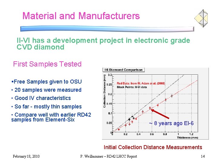
Material and Manufacturers II-VI has a development project in electronic grade CVD diamond First Samples Tested §Free Samples given to OSU • 20 samples were measured • Good IV characteristics • So far - mostly thin samples • Compare well with earlier RD 42 samples from Element-Six ~ 8 years ago El-6 Initial Collection Distance Measurements February 18, 2010 P. Weilhammer – RD 42 LHCC Report 14

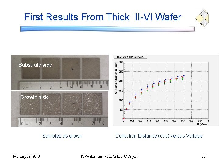
Recent Material from II-VI Substrate side • As grown, ~1. 5 mm thick • Surprisingly good results – ccd uniform across all samples – 220 -230 µm @ 0. 7 V/µm, not saturated (Error in metallization, CCD lower limit) • Working with II-VI to optimize further – Take off substrate side in steps – Go to higher fields • Ultimate goal : – 500µm thick, 300µm CCD, – 300 -400 CHF/cm 2 § Not yet committed to regular sales February 18, 2010 P. Weilhammer – RD 42 LHCC Report 15

First Results From Thick II-VI Wafer Substrate side Growth side Samples as grown February 18, 2010 Collection Distance (ccd) versus Voltage P. Weilhammer – RD 42 LHCC Report 16

Radiation Hardness of CVD Material Important Parameters for Radiation Hardness: - binding energy - displacement energy - elastic, inelastic, total cross section February 18, 2010 P. Weilhammer – RD 42 LHCC Report 17

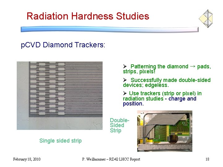
Radiation Hardness Studies p. CVD Diamond Trackers: Ø Patterning the diamond → pads, strips, pixels! Ø Successfully made double-sided devices; edgeless. Ø Use trackers (strip or pixel) in radiation studies - charge and position. Double. Sided Strip Single sided strip February 18, 2010 P. Weilhammer – RD 42 LHCC Report 18

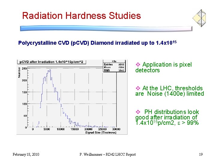
Radiation Hardness Studies Polycrystalline CVD (p. CVD) Diamond irradiated up to 1. 4 x 10¹⁵ v Application is pixel detectors v At the LHC, thresholds are Noise (1400 e) limited v PH distributions look good after irradiation of 1. 4 x 10¹⁵ p/cm 2, e > 99% February 18, 2010 P. Weilhammer – RD 42 LHCC Report 19

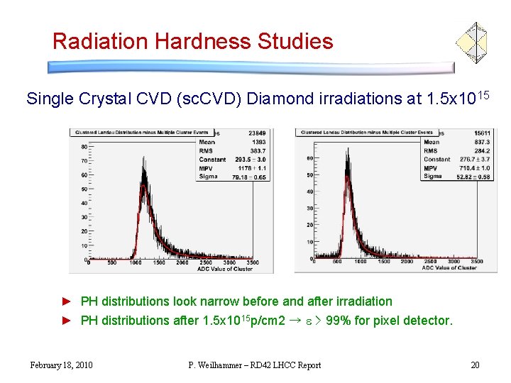
Radiation Hardness Studies Single Crystal CVD (sc. CVD) Diamond irradiations at 1. 5 x 10¹⁵ ► PH distributions look narrow before and after irradiation ► PH distributions after 1. 5 x 10¹⁵ p/cm 2 → e > 99% for pixel detector. February 18, 2010 P. Weilhammer – RD 42 LHCC Report 20

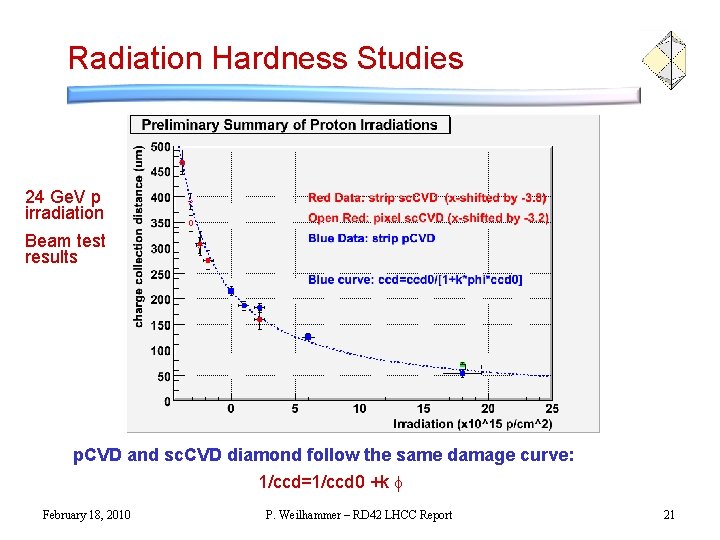
Radiation Hardness Studies 24 Ge. V p irradiation Beam test results p. CVD and sc. CVD diamond follow the same damage curve: 1/ccd=1/ccd 0 +k f February 18, 2010 P. Weilhammer – RD 42 LHCC Report 21

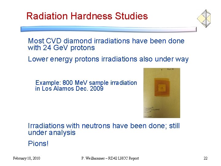
Radiation Hardness Studies Most CVD diamond irradiations have been done with 24 Ge. V protons Lower energy protons irradiations also under way Example: 800 Me. V sample irradiation in Los Alamos Dec. 2009 Irradiations with neutrons have been done; still under analysis Pions! February 18, 2010 P. Weilhammer – RD 42 LHCC Report 22

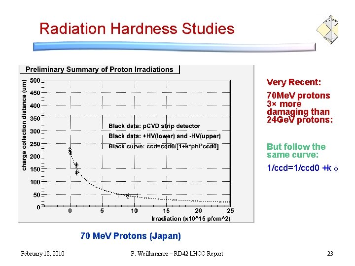
Radiation Hardness Studies Very Recent: 70 Me. V protons 3× more damaging than 24 Ge. V protons: But follow the same curve: 1/ccd=1/ccd 0 +k f 70 Me. V Protons (Japan) February 18, 2010 P. Weilhammer – RD 42 LHCC Report 23

Radiation Hardness Studies-Pions • Need pions in n x 100 Me. V ballpark – Applied for beam at PSI (with RD-50) • Use sc. CVD to maximize damage effect – Negotiate very simple pion beam line at LANL • If approved, could reach s. LHC fluences • Quick evaluation with strip detectors in 800 Me. V proton beam February 18, 2010 P. Weilhammer – RD 42 LHCC Report 24

p. CVD and sc. CVD Pixel Detectors Issues: - Signal - Noise, threshold - Charge sharing, signal over threshold February 18, 2010 P. Weilhammer – RD 42 LHCC Report 25

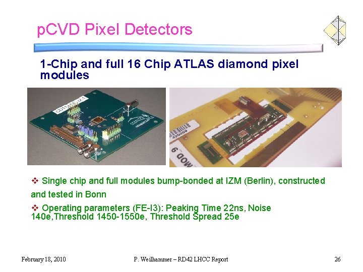
p. CVD Pixel Detectors 1 -Chip and full 16 Chip ATLAS diamond pixel modules v Single chip and full modules bump-bonded at IZM (Berlin), constructed and tested in Bonn v Operating parameters (FE-I 3): Peaking Time 22 ns, Noise 140 e, Threshold 1450 -1550 e, Threshold Spread 25 e February 18, 2010 P. Weilhammer – RD 42 LHCC Report 26

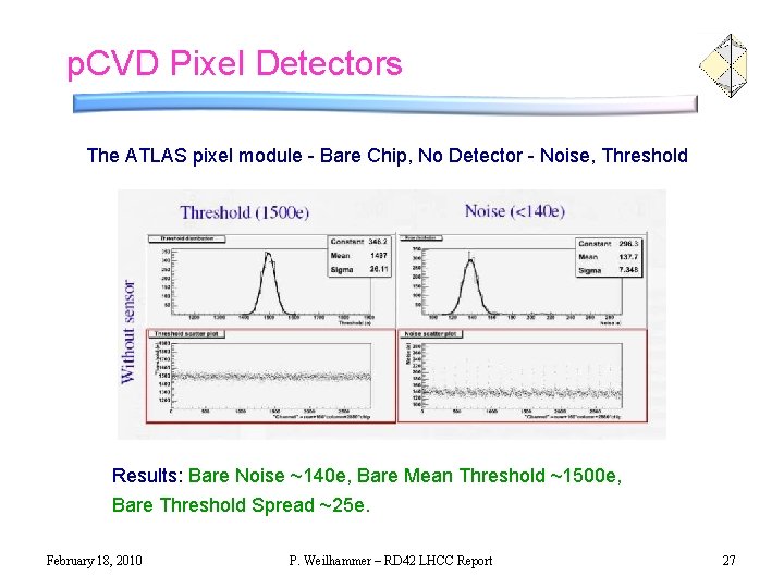
p. CVD Pixel Detectors The ATLAS pixel module - Bare Chip, No Detector - Noise, Threshold Results: Bare Noise ~140 e, Bare Mean Threshold ~1500 e, Bare Threshold Spread ~25 e. February 18, 2010 P. Weilhammer – RD 42 LHCC Report 27

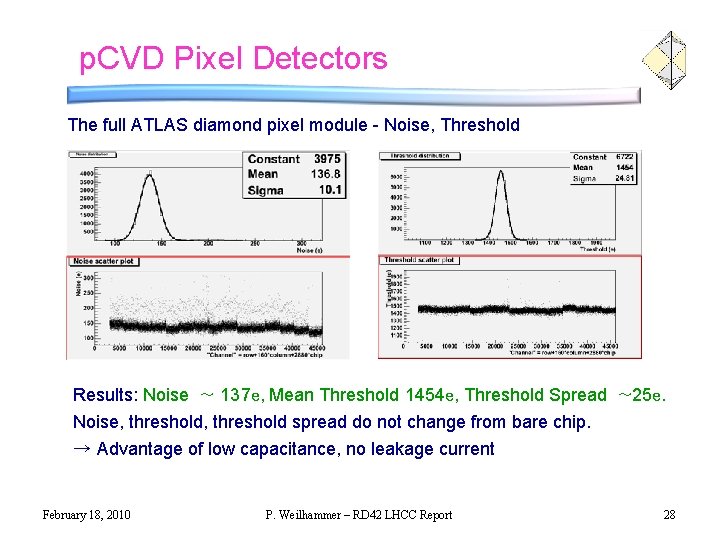
p. CVD Pixel Detectors The full ATLAS diamond pixel module - Noise, Threshold Results: Noise ~ 137 e, Mean Threshold 1454 e, Threshold Spread ~25 e. Noise, threshold spread do not change from bare chip. → Advantage of low capacitance, no leakage current February 18, 2010 P. Weilhammer – RD 42 LHCC Report 28

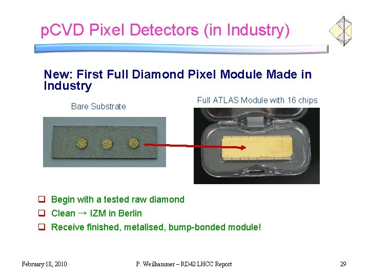
p. CVD Pixel Detectors (in Industry) New: First Full Diamond Pixel Module Made in Industry Bare Substrate Full ATLAS Module with 16 chips q Begin with a tested raw diamond q Clean → IZM in Berlin q Receive finished, metalised, bump-bonded module! February 18, 2010 P. Weilhammer – RD 42 LHCC Report 29

Applications in Experiments The 4 big experiments around LHC : CMS, ALICE, LHCb, and ATLAS have projects for beam monitoring and high luminosity upgrades involving sc. CVD and p. CVD diamond detector substrates. Also LHC control is working on a CVD diamond beam control detector. In the following few slides I comment on some ATLAS implementations and plans February 18, 2010 P. Weilhammer – RD 42 LHCC Report 30

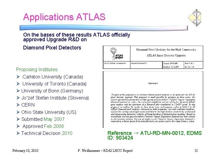
Applications ATLAS On the bases of these results ATLAS officially approved Upgrade R&D on Diamond Pixel Detectors Proposing Institutes: Ø Carleton University (Canada) Ø University of Toronto (Canada) Ø University of Bonn (Germany) Ø Joˇzef Stefan Institute (Slovenia) Ø CERN Ø Ohio State University (US) Ø Submitted May 2007 Ø Approved Feb 2008 Ø Technical Decision 2010 February 18, 2010 Reference → ATU-RD-MN-0012, EDMS ID: 903424 P. Weilhammer – RD 42 LHCC Report 31

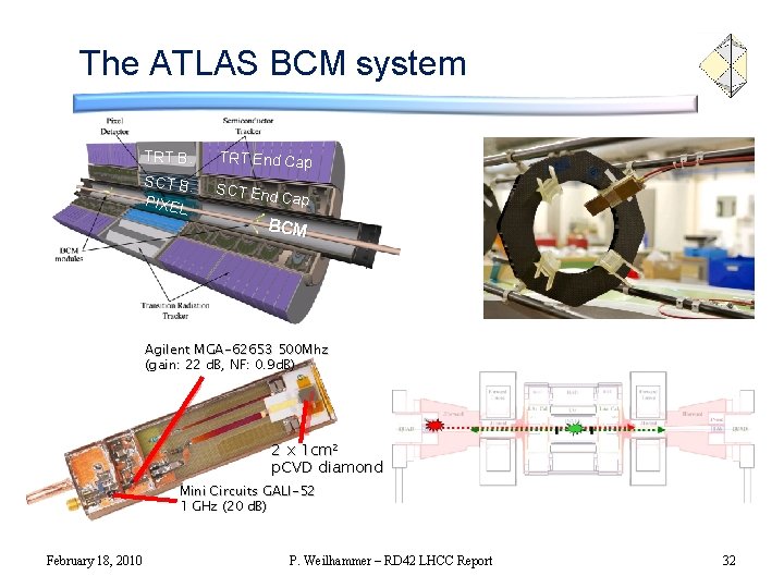
The ATLAS BCM system TRT B. SCT B. PIXEL TRT End Cap SCT End Cap BCM Agilent MGA-62653 500 Mhz (gain: 22 d. B, NF: 0. 9 d. B) 2 x 1 cm 2 p. CVD diamond Mini Circuits GALI-52 1 GHz (20 d. B) February 18, 2010 P. Weilhammer – RD 42 LHCC Report 32

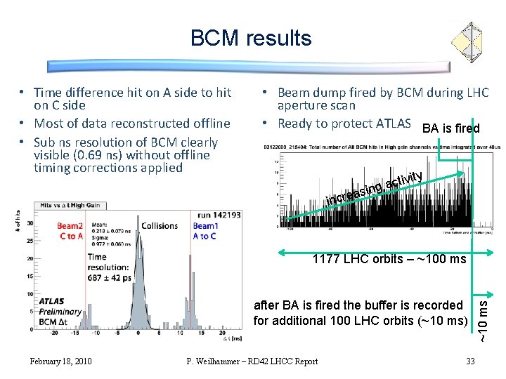
BCM results • Time difference hit on A side to hit on C side • Most of data reconstructed offline • Sub ns resolution of BCM clearly visible (0. 69 ns) without offline timing corrections applied • Beam dump fired by BCM during LHC aperture scan • Ready to protect ATLAS BA is fired ity ctiv a g in as e r c in after BA is fired the buffer is recorded for additional 100 LHC orbits (~10 ms) February 18, 2010 P. Weilhammer – RD 42 LHCC Report 33 ~10 ms 1177 LHC orbits – ~100 ms

REQUESTS FROM CERN The RD 42 Role at CERN v Irradiations, development of new manufacturers, sample procurement, test beams v Central facilities for all experiments this worked for BCM’s v CERN Group in RD 42 to be strengthened RD 42 Request to CERN/LHCC v RD 42 is supported by many national agencies: continuation of official recognition by CERN critical 50 k. CHF from CERN/ ~200 k. CHF from outside CERN v RD 42 requires access to CERN facilities: maintain the present 20 m 2 of lab space (test setups, detector prep, . . . ) maintain present office space test beam time RD 42 and CERN play a critical role in diamond development February 18, 2010 P. Weilhammer – RD 42 LHCC Report 34

Summary v Further Progress in Material Quality and New Manufacturers p. CVD - 320 μm collection distance diamond attained in wafer growth sc. CVD – Radiation Hardness measured; pixel detectors in preparation One new CVD diamond manufacturer has come onto the scene. Produce very good material. v Radiation Hardness of Diamond Trackers established; further measurements essential (pions) v Diamond Pixel Detectors Successfully tested a complete ATLAS module and sc. CVD module Full modules in production. Industrial production in place. Diamond R&D Approved by ATLAS for IBL and LHC Upgrade v Beam Conditions Monitoring Application of diamond successful in Ba. Bar, CDF, Alice, ATLAS, CMS, LHCb…. February 18, 2010 P. Weilhammer – RD 42 LHCC Report 35

Additional Material February 18, 2010 P. Weilhammer – RD 42 LHCC Report 36

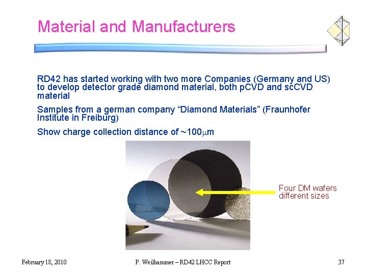
Material and Manufacturers RD 42 has started working with two more Companies (Germany and US) to develop detector grade diamond material, both p. CVD and sc. CVD material Samples from a german company “Diamond Materials” (Fraunhofer Institute in Freiburg) Show charge collection distance of ~100 mm Four DM wafers different sizes February 18, 2010 P. Weilhammer – RD 42 LHCC Report 37

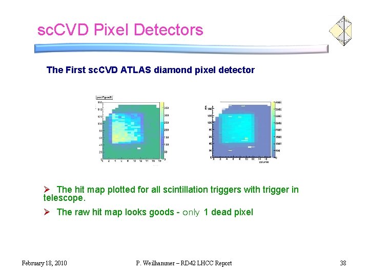
sc. CVD Pixel Detectors The First sc. CVD ATLAS diamond pixel detector Ø The hit map plotted for all scintillation triggers with trigger in telescope. Ø The raw hit map looks goods - only 1 dead pixel February 18, 2010 P. Weilhammer – RD 42 LHCC Report 38

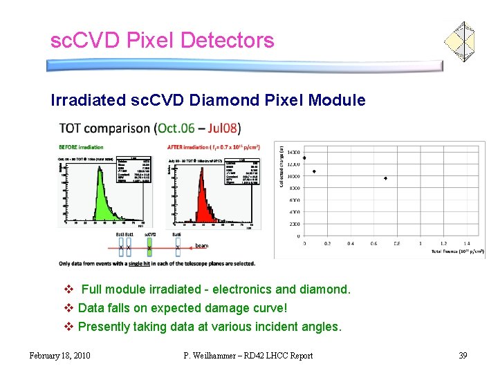
sc. CVD Pixel Detectors Irradiated sc. CVD Diamond Pixel Module v Full module irradiated - electronics and diamond. v Data falls on expected damage curve! v Presently taking data at various incident angles. February 18, 2010 P. Weilhammer – RD 42 LHCC Report 39

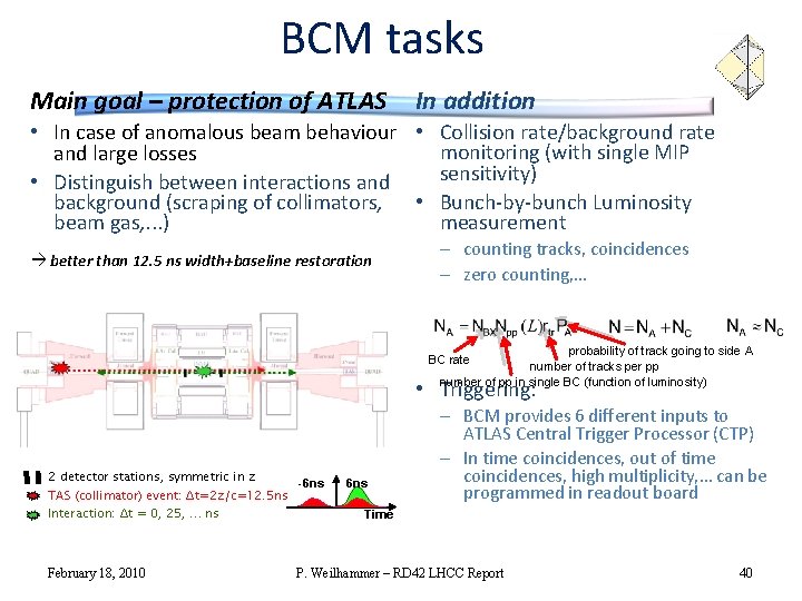
BCM tasks Main goal – protection of ATLAS In addition • In case of anomalous beam behaviour • Collision rate/background rate monitoring (with single MIP and large losses sensitivity) • Distinguish between interactions and background (scraping of collimators, • Bunch-by-bunch Luminosity measurement beam gas, . . . ) better than 12. 5 ns width+baseline restoration – counting tracks, coincidences – zero counting, … probability of track going to side A number of tracks per pp number of pp in single BC (function of luminosity) BC rate • Triggering: 2 detector stations, symmetric in z TAS (collimator) event: Δt=2 z/c=12. 5 ns Interaction: Δt = 0, 25, … ns February 18, 2010 -6 ns – BCM provides 6 different inputs to ATLAS Central Trigger Processor (CTP) – In time coincidences, out of time coincidences, high multiplicity, … can be programmed in readout board Time P. Weilhammer – RD 42 LHCC Report 40

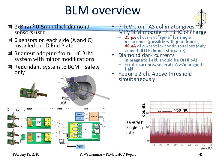
BLM overview 8 x 8 mm 2 0. 5 mm thick diamond sensors used 6 sensors on each side (A and C) installed on ID End Plate Readout adopted from LHC BLM system with minor modifications Redundant system to BCM – safety only • 7 Te. V p on TAS collimator gives ~1 MIP/BLM module ~1 f. C of charge – 25 p. A of current “spike” for single occurrence (possible with pilot bunch) – 40 n. A of current for continuous loss (only when full LHC bunch structure) • Diamond dark currents – In magnetic field, should be O(10 p. A) – Erratic currents, several n. A w/o magnetic field • Require 2 ch. Above threshold simultaneously BCM counts BLM ~50 n. A several h single ch. rates … February 18, 2010 P. Weilhammer – RD 42 LHCC Report 41