Diamond Detectors Ltd Diamond Detectors Introduction to DDL

- Slides: 28

Diamond Detectors Ltd Diamond Detectors Introduction to DDL Facilities / Investments Markets / Applications Partnerships / Projects DDL Proprietary Contact Technology Alex Brown Sales & Marketing * Diamond Detectors Limited 1

Diamond Detectors Ltd Diamond Detectors Introduction to DDL Facilities / Investments Markets / Applications Partnerships / Projects DDL Proprietary Contact Technology Alex Brown Sales & Marketing * Diamond Detectors Limited 2

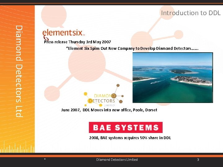
Introduction to DDL Diamond Detectors Ltd Press release Thursday 3 rd May 2007 “Element Six Spins Out New Company to Develop Diamond Detectors……. June 2007, DDL Moves into new office, Poole, Dorset 2008, BAE systems acquires 50% share in DDL * Diamond Detectors Limited 3

Diamond Detectors Ltd Diamond Detectors Introduction to DDL Facilities / Investments Markets / Applications Partnerships / Projects DDL Proprietary Contact Technology Alex Brown Sales & Marketing * Diamond Detectors Limited 4

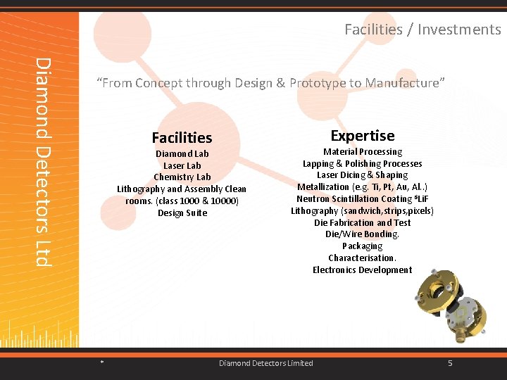
Facilities / Investments Facilities Expertise Diamond Lab Laser Lab Chemistry Lab Lithography and Assembly Clean rooms. (class 1000 & 10000) Design Suite * Material Processing Lapping & Polishing Processes Laser Dicing & Shaping Metallization (e. g. Ti, Pt, Au, Al. . ) Neutron Scintillation Coating 6 Li. F Lithography (sandwich, strips, pixels) Die Fabrication and Test Die/Wire Bonding. Packaging Characterisation. Electronics Development Diamond Detectors Limited Diamond Detectors Ltd “From Concept through Design & Prototype to Manufacture” 5

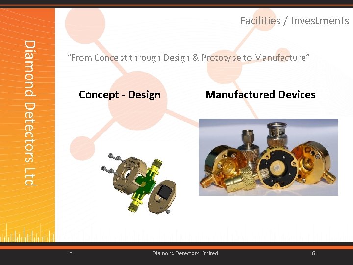
Facilities / Investments Concept - Design * Diamond Detectors Ltd “From Concept through Design & Prototype to Manufacture” Manufactured Devices Diamond Detectors Limited 6

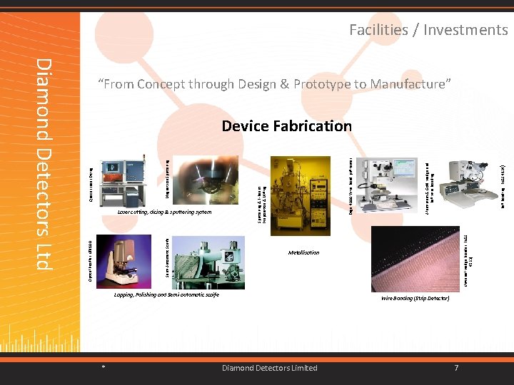
Aluminium & Gold wedge and ball wire bonding Dage 4000 Wire bond pull tester Metallisation Lapping, Polishing and Semi-automatic scaife * Universal wedge bonder (K&S 4523) Optical Profiler NT 9100 Semi Automatic Scaife Laser cutting, dicing & sputtering system Sputtering & E-Beam Evaporation & Milling Quazer Laser Dicing Magnetron Sputtering Device Fabrication Diamond Detectors Ltd “From Concept through Design & Prototype to Manufacture” Wire Bonding (Strip Detector) Diamond Detectors Limited 7 ball bonding (K&S 4124) Facilities / Investments

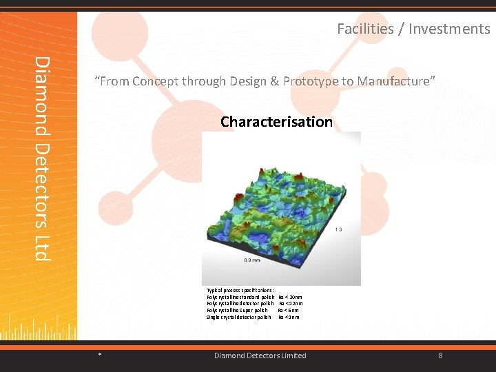
Facilities / Investments Characterisation Diamond Detectors Ltd “From Concept through Design & Prototype to Manufacture” Typical process specifications : Polycrystalline standard polish Ra < 20 nm Polycrystalline detector polish Ra < 12 nm Polycrystalline Super polish Ra < 5 nm Single crystal detector polish Ra < 1 nm * Diamond Detectors Limited 8

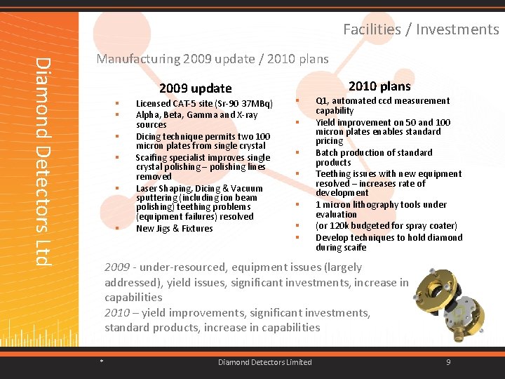
Facilities / Investments 2009 update Licensed CAT-5 site (Sr-90 37 MBq) Alpha, Beta, Gamma and X-ray sources Dicing technique permits two 100 micron plates from single crystal Scaifing specialist improves single crystal polishing – polishing lines removed Laser Shaping, Dicing & Vacuum sputtering (including ion beam polishing) teething problems (equipment failures) resolved New Jigs & Fixtures 2010 plans Q 1, automated ccd measurement capability Yield improvement on 50 and 100 micron plates enables standard pricing Batch production of standard products Teething issues with new equipment resolved – increases rate of development 1 micron lithography tools under evaluation (or 120 k budgeted for spray coater) Develop techniques to hold diamond during scaife 2009 - under-resourced, equipment issues (largely addressed), yield issues, significant investments, increase in capabilities 2010 – yield improvements, significant investments, standard products, increase in capabilities * Diamond Detectors Limited Diamond Detectors Ltd Manufacturing 2009 update / 2010 plans 9

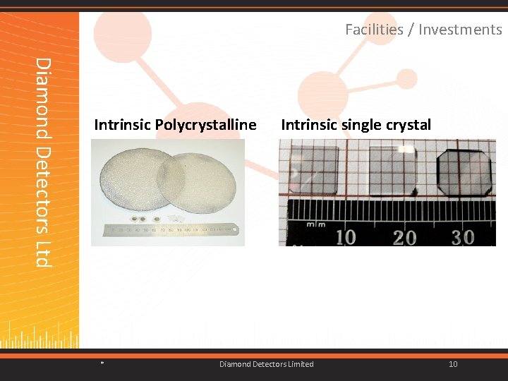
Facilities / Investments * Intrinsic single crystal Diamond Detectors Limited Diamond Detectors Ltd Intrinsic Polycrystalline 10

Diamond Detectors Ltd Diamond Detectors Introduction to DDL Facilities / Investments Markets / Applications Partnerships / Projects DDL Proprietary Contact Technology Alex Brown Sales & Marketing * Diamond Detectors Limited 11

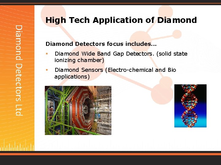
Diamond Detectors Ltd Diamond Detectors focus includes. . . Diamond Wide Band Gap Detectors. (solid state ionizing chamber) Diamond Sensors (Electro-chemical and Bio applications) Diamond Detectors Ltd High Tech Application of Diamond

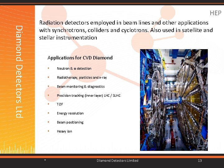
HEP Applications for CVD Diamond * Neutron & α detection Radiotherapy, particles and x-ray Beam monitoring & diagnostics Precision tracking (inner layer) LHC / SLHC TOF Energy resolution Beam positioning Heavy ion Diamond Detectors Limited Diamond Detectors Ltd Radiation detectors employed in beam lines and other applications with synchrotrons, colliders and cyclotrons. Also used in satellite and stellar instrumentation 13

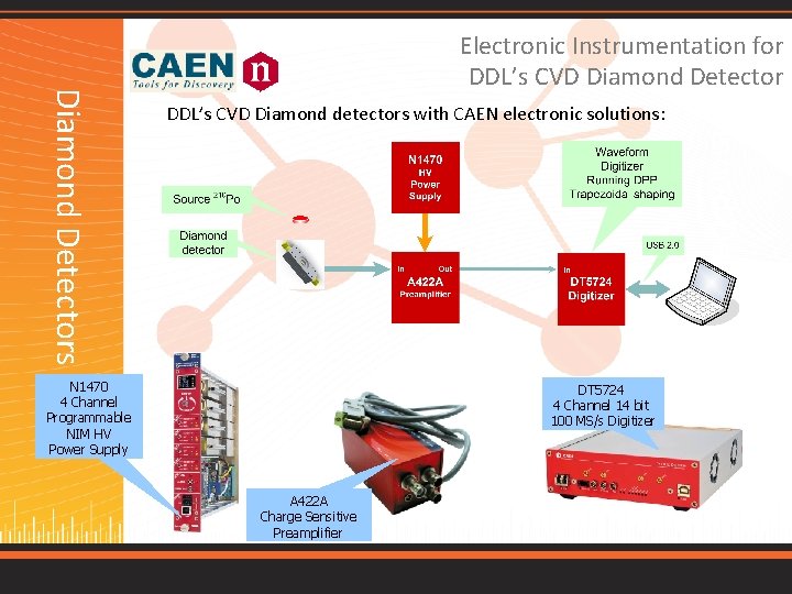
DDL’s CVD Diamond detectors with CAEN electronic solutions: N 1470 4 Channel Programmable NIM HV Power Supply DT 5724 4 Channel 14 bit 100 MS/s Digitizer A 422 A Charge Sensitive Preamplifier Diamond Detectors Ltd Electronic Instrumentation for DDL’s CVD Diamond Detector

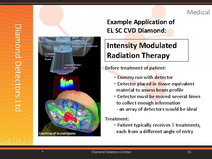
Medical Intensity Modulated Radiation Therapy Before treatment of patient: Diamond Detectors Ltd Example Application of EL SC CVD Diamond: • Dummy run with detector • Detector placed in tissue equivalent material to assess beam profile • Detector must be moved several times to collect enough information - an array of detectors would be ideal Treatment: • Patient typically receives 3 treatments, each from a different angle of entry * Diamond Detectors Limited 15

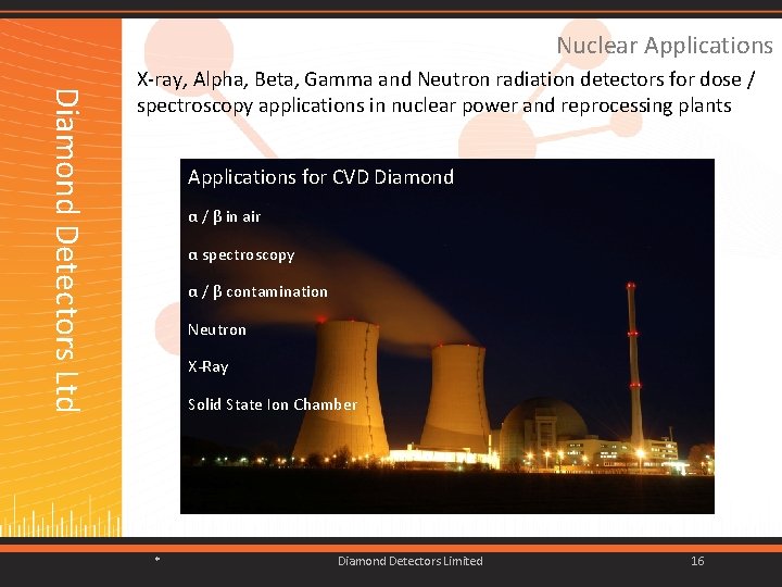
Nuclear Applications for CVD Diamond α / β in air α spectroscopy α / β contamination Neutron X-Ray Solid State Ion Chamber * Diamond Detectors Limited Diamond Detectors Ltd X-ray, Alpha, Beta, Gamma and Neutron radiation detectors for dose / spectroscopy applications in nuclear power and reprocessing plants 16

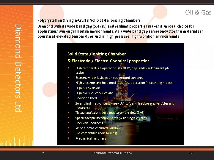
Oil & Gas Solid State /Ionizing Chamber & Electrode / Electro-Chemical properties * High temperature operation (>>300 C, negligible dark current p. A scale) Extremely low leakage or background currents. High electron and hole motilities (fast operation in counting modes) High break down. High thermal conductivity Radiation hard. Solar blind (response to deep UV, soft and hard x-rays, particles and neutrons) Tissue equivalent dose measurement (low Z =6) Spectroscopic measurements (with single crystal) Chemical inertness. Wide electro-chemical window Bio-compatible (non-fouling) Mechanical hardness Diamond Detectors Limited Diamond Detectors Ltd Polycrystalline & Single-Crystal Solid-State Ionizing Chambers Diamond with its wide band gap (5. 47 ev) and resilient properties makes it an ideal choice for applications working in hostile environments. As a wide band gap semi-conductor the material can operate at elevated temperature and in high pressure, high vibration environments 17

Projects Diamond Detectors Ltd Mike Bentley, York University , (Fair beamline Instrumentation) Richard Hugtenburg, Swansea University, (Medical Dosimeters) Prof. Peter Winlove, Exeter University, (Knowledge Transfer Program for diamond based bio/chemical sensors) Japp Velthuis, Bristol University, (RD 42 member) Case Studentship for GHz fast counting applications in Civil Nuclear and Particle Therapy Darren Caruana, UCL, BDD electrodes for pollen identification and counting Various industrial partners across the DDL markets * Diamond Detectors Limited 18

Diamond Detectors Ltd Diamond Detectors Introduction to DDL Facilities / Investments Markets / Applications Partnerships / Projects DDL Proprietary Contact Technology Alex Brown Sales & Marketing * Diamond Detectors Limited 19

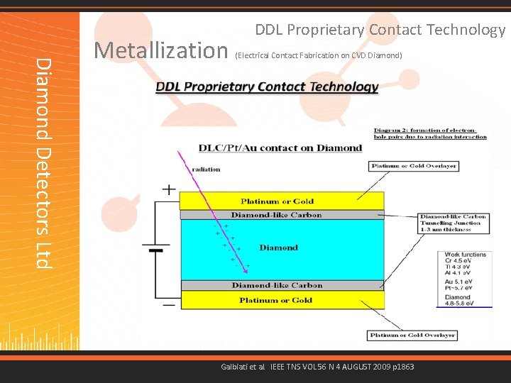
(Electrical Contact Fabrication on CVD Diamond) Diamond Detectors Ltd Metallization DDL Proprietary Contact Technology Diamond Detectors Limited (DDL) has patented an innovative metallization technique to maximize CVD diamond performance. Here we seek to highlight the issues and describe the solution. The development of CVD Diamond has made possible many new applications for detecting and sensing. However, manufacturing semiconductor devices in diamond present some interesting challenges due to diamond’s unique characteristics. Traditional or inadequate contact fabrication may result in poor mechanical adhesion, polarization effects and unrepeatable results. Mechanical Adhesion Specifically, the mechanical adhesion of the metal chosen as electrode on the diamond surface. A flatter smoother surface presents fewer adhesion points. When a metal is thermally evaporated on diamond it may not adhere and it could peel off after a short period of time with the consequent deterioration of the electrical signal measured and therefore a decrease in the lifetime of the device. Mechanical adhesion is a function of the diamond / contact interface. Polarization Effects Polarization phenomena occur when electric currents pass through diamond if the electrical contact is not able to extract and inject electrons fast enough. In this case, the neutrality of the crystal after the passage of ionizing nuclear radiations is not restored in the time interval between two consecutive events. As a result, charge accumulation occurs within the crystal and immobile carriers establish an electric field which acts in a direction opposite to the applied field produced by the external bias voltage V. The minimisation of polarization effects requires optimal injecting contacts. Repeatable Results If a device is to be commercially viable it should be consistent and stable in a variety of environmental conditions. Requires stable and resilient contacts. Historically, there have been three main approaches to fabricate good electrical contacts on diamond: 1. Damaging the diamond surface in order to disrupt the sp 3 bonding. 2. Using carbide forming metals like titanium or chromium to create a hybrid metal-diamond interface material. 3. Doping of diamond during growth or using ion implantation. For example, to prepare good injecting contacts, several metals were used by Kozlov et al. , for hole injection they used Ag, Au, Pt or C deposition, aluminium or boron implantation, for electron injection P, Li or C. Galbiati et al. IEEE TNS VOL 56 N 4 AUGUST 2009 p 1863

(Electrical Contact Fabrication on CVD Diamond) Galbiati et al. IEEE TNS VOL 56 N 4 AUGUST 2009 p 1863 Diamond Detectors Ltd Metallization DDL Proprietary Contact Technology

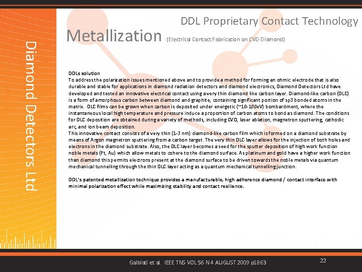
(Electrical Contact Fabrication on CVD Diamond) Diamond Detectors Ltd Metallization DDL Proprietary Contact Technology DDLs solution To address the polarization issues mentioned above and to provide a method forming an ohmic electrode that is also durable and stable for applications in diamond radiation detectors and diamond electronics, Diamond Detectors Ltd have developed and tested an innovative electrical contact using a very thin diamond like carbon layer. Diamond-like carbon (DLC) is a form of amorphous carbon between diamond and graphite, containing significant portion of sp 3 bonded atoms in the matrix. DLC films can be grown when carbon is deposited under energetic (~10 -100 e. V) bombardment, where the instantaneous local high temperature and pressure induce a proportion of carbon atoms to bond as diamond. The conditions for DLC deposition are obtained during a variety of methods, including CVD, laser ablation, magnetron sputtering, cathodic arc, and ion beam deposition. This innovative contact consists of a very thin (1 -3 nm) diamond-like carbon film which is formed on a diamond substrate by means of Argon magnetron sputtering from a carbon target. The very thin DLC layer allows for the injection of both holes and electrons in the diamond substrate. Also, the DLC layer becomes a seed for the sputter deposition of high work function noble metals (Pt, Au) which allow metals to cohere to the diamond surface. As platinum and gold have a higher work function than diamond this permits electrons present at the diamond surface to be driven towards the noble metals via quantum mechanical tunnelling through the thin DLC layer acting as a quantum mechanical tunnelling junction. DDL’s patented metallization technique provides a manufacturable, high adherence diamond / contact interface with minimal polarization effect while maximizing stability and contact resilience. Galbiati et al. IEEE TNS VOL 56 N 4 AUGUST 2009 p 1863 22

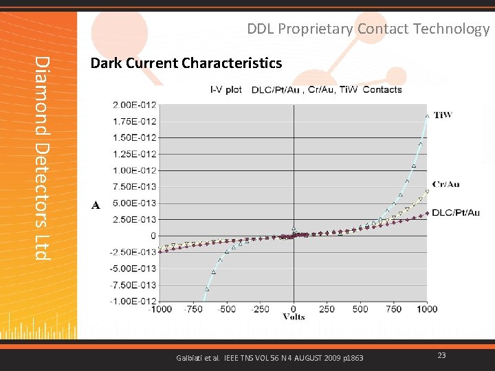
DDL Proprietary Contact Technology Galbiati et al. IEEE TNS VOL 56 N 4 AUGUST 2009 p 1863 Diamond Detectors Ltd Dark Current Characteristics 23

Diamond Detectors Ltd REFERENCES: Bergonzo et al. , Diamond and Related Materials, Volume 10, Issues 3 -7, March-July (2001), 631 -638 J. H. Kaneko et al. / Nuclear Instruments and Methods in Physics Research A 505 (2003) 187– 190 Pomorski et al. , Phys. Stat. Sol. (a) 202, No. 11 (2005) Gianluca Verona-Rinati “Single crystal CVD diamond neutron detectors in a p-type/intrinsic/metal layered structure” , http: //www-norhdia. gsi. de/talks/4 th/G_Verona-Rinati. pdf Galbiati et al. “Performance of Monocrystalline Diamond Radiation Detectors Fabricated Using Ti. W, Cr/Au and a Novel Ohmic DLC/Pt/Au Electrical Contact” IEEE TNS VOL 56 N 4 AUGUST 2009 p 1863 Angelone et al. : “NEUTRON DETECTORS BASED UPON ARTIFICIAL SINGLE CRYSTAL DIAMOND” IEEE TRANSACTIONS ON NUCLEAR SCIENCE, VOL. 56, NO. 4, AUGUST 2009 pp. 2275 -2279 Almaviva et al. : “Thermal and fast neutron detection in chemical vapor deposition single-crystal diamond detectors” J. Appl. Phys. 103, 054501 2008 G. J. Schmid et al. “A neutron sensor based on single crystal CVD diamond”, Nuclear Instruments and Methods in Physics Research A 527 (2004) 554– 561 M. Pillon, M. Angelone, A. V. Krasilnikov, Nucl. Instr. and Meth. Phys. Res. B 101 (1995) 473.

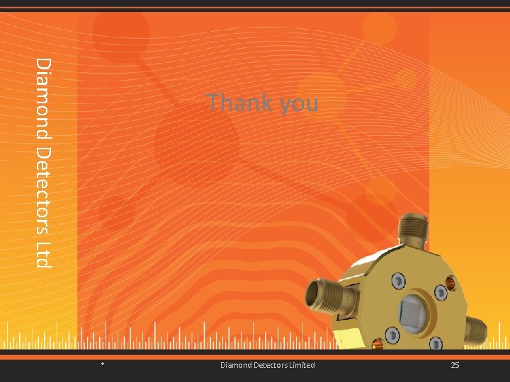
25 Diamond Detectors Limited * Diamond Detectors Ltd Thank you

Diamond Detectors Ltd Collaborating Opportunities ? Custom design and prototype manufacture. Let us help you develop a resilient detector/sensor technology for your application using our design tools, facilities and experience in collaboration with your R&D team. Prototype to Product (cost engineering, batch processing and test) * Diamond Detectors Limited 26

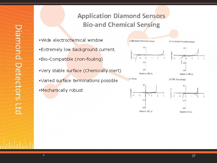
Wide electrochemical window Extremely low background current. Bio-Compatible (non-fouling) Very stable surface (Chemically inert) Varied surface terminations possible Mechanically robust * Diamond Detectors Ltd Application Diamond Sensors Bio-and Chemical Sensing 27

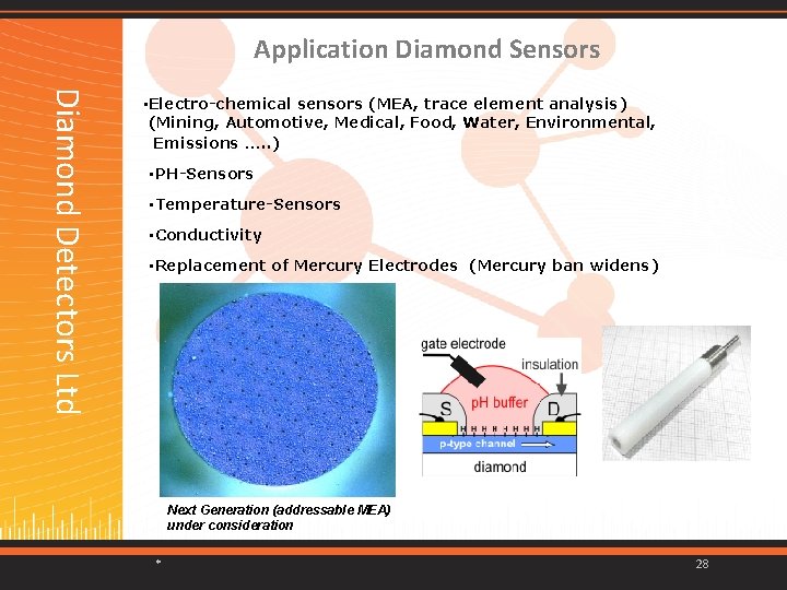
Application Diamond Sensors • PH-Sensors • Temperature-Sensors • Conductivity • Replacement of Mercury Electrodes (Mercury ban widens) Diamond Detectors Ltd • Electro-chemical sensors (MEA, trace element analysis) (Mining, Automotive, Medical, Food, Water, Environmental, Emissions …. . ) Next Generation (addressable MEA) under consideration * 28