Frontier Detectors for Frontier Physics 13 TH PISA

- Slides: 2
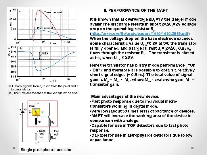
Frontier Detectors for Frontier Physics “ 13 -TH PISA MEETING ON ADVANCED DETECTORS” A NEW DETECTOR CONCEPT FOR SILICON PHOTOMULTIPLIERS A. Sadigov 1, F. Ahmadov 1, A. Ariffin 2, S. Khorev 2, Z. Sadygov 1, 3, S. Suleymanov 1, F. Zerrouk 2 1 - National Nuclear Research Center, Baku, Azerbaijan; 2 - Zecotek Photonics Inc. ; 3 - Joint Institute for Nuclear Research, Dubna, Russia The silicon photomultiplier (Si. PM), also named as the micro-pixel avalanche photodiode (MAPD) was invented in 1996 year (Z. Sadygov…. . , Russian patent № 2102820, priority from 10. 1996). The device comprises an array of small p-n - junctions (pixels) with individual quenching resistors. However, this design has a high specific capacitance (about 30 p. F/mm 2 ), which limits the sensitive area of the MAPD. Here we present a new Si. PM on basis of a Micro-pixel Avalanche Photo-Transistor (MAPT). I. DESIGN OF THE MAPT The MAPT Comprises an array of micro phototransistors with individual ballast resistors Rt, the base electrodes of which are connected to the pixels with quenching resistors Rp (Z. Sadygov and A. Sadigov. Russian patent № 2528107, a priority from 04. 16. 2013). Each pixel the MAPT consists of two parts: an avalanche region and a microtransistor region. Area of the micro-transistor region is about 3µ× 3µ which is about 1÷ 5% of the pixel area. Therefore, the MAPT device has 30 ÷ 50 times lower capacitance than known Si. PMs.
II. PERFORMANCE OF THE MAPT It is known that at overvoltage Up=1 V the Geiger mode avalanche discharge results in about 2× Up=2 V voltage drop on the quenching resistor Rp (http: //arxiv. org/ftp/arxiv/papers/1410. 2619. pdf). When the voltage drop on the base electrode exceeds some characteristic value Uc. v≈0. 8 V at t=t, the transistor is fully opened, and a large current Jtr=(2× Up-0. 8)/Rtr flows through the resistor Rtr. The transistor is closed at t=t 2 when Uc. v ≤ 0. 8 V. (a. ) Photo signals forms, taken from the pixel and a micro-transistor. (b. ) The time dependence of the voltage at the pixel. Here the transistor has binary mode performance ( "On - Off"), and therefore it is possible to obtain a relatively short signal edges (~ 0. 5 ns). The total value of signal gain is Mp = Mav × Mtr, where Mav - avalanche gain, Mtr – transistor gain. Main advantages of the new device. • Fast photo response due to individual microtransistors working in digital mode. • Very low (about 50 times less) capacitance of devices. • MAPT will increase the working area of the device in comparison with analogs. • Capable for use in TOF detectors due to fast photo response. • Capable for use in astrophysics detectors due to low capacitance.