CT 455 Computer Organization Logic gate CS 1103




- Slides: 76
CT 455: Computer Organization Logic gate CS 1103 Chapter 1: Introduction
Lecture 4: Logic Gates and Circuits § Logic Gates v The Inverter v The AND Gate v The OR Gate v The NAND Gate v The NOR Gate v The XNOR Gate § § § CS 1104 -4 Drawing Logic Circuit Analysing Logic Circuit Propagation Delay Lecture 4: Introduction to Logic Gates 2
Lecture 4: Logic Gates and Circuits § Universal Gates: NAND and NOR v NAND Gate v NOR Gate § § § CS 1104 -4 Implementation using NAND Gates Implementation using NOR Gates Implementation of SOP Expressions Implementation of POS Expressions Positive and Negative Logic Integrated Circuit Logic Families Lecture 4: Introduction to Logic Gates 3
Digital (logic) Elements: Gates Digital devices or gates have one or more inputs and produce an output that is a function of the current input value(s). All inputs and outputs are binary and can only take the values 0 or 1 A gate is called a combinational circuit because the output only depends on the current input combination. Digital circuits are created by using a number of connected gates such as the output of a gate is connected to to the input of one or more gates in such a way to achieve specific outputs for input values. Digital or logic design is concerned with the design of such circuits. CS 1103 Chapter 1: Introduction
Introduction Hardware consists of a few simple building blocks n These are called logic gates AND, OR, NOT, … NAND, NOR, XOR, … Logic gates are built using transistors NOT gate can be implemented by a single transistor AND gate requires 3 transistors Transistors are the fundamental devices Pentium consists of 3 million transistors Compaq Alpha consists of 9 million transistors Now we can build chips with more than 100 million transistors CS 1103 Chapter 1: Introduction
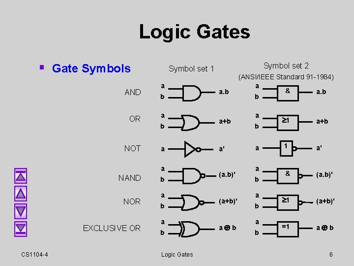
Logic Gates § Gate Symbols AND OR NOT a b a a NAND NOR EXCLUSIVE OR CS 1104 -4 Symbol set 2 Symbol set 1 b a b Logic Gates a. b a+b a' (a. b)' (a+b)' a b (ANSI/IEEE Standard 91 -1984) a & a. b b a a b a b 1 a+b 1 a' & (a. b)' 1 (a+b)' =1 a b 6
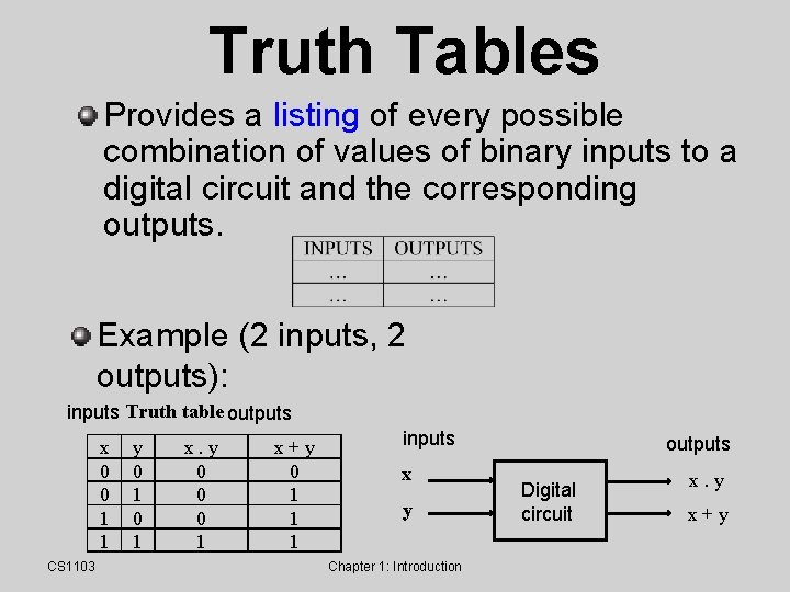
Truth Tables Provides a listing of every possible combination of values of binary inputs to a digital circuit and the corresponding outputs. Example (2 inputs, 2 outputs): inputs Truth table outputs x 0 0 1 1 CS 1103 y 0 1 x. y 0 0 0 1 x+y 0 1 1 1 inputs x y Chapter 1: Introduction outputs Digital circuit x. y x+y
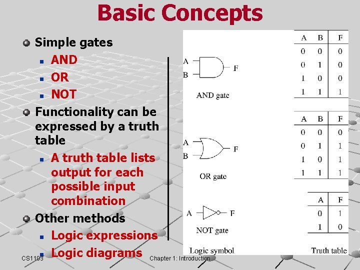
Basic Concepts Simple gates n AND n OR n NOT Functionality can be expressed by a truth table n A truth table lists output for each possible input combination Other methods n Logic expressions n Logic diagrams CS 1103 Chapter 1: Introduction
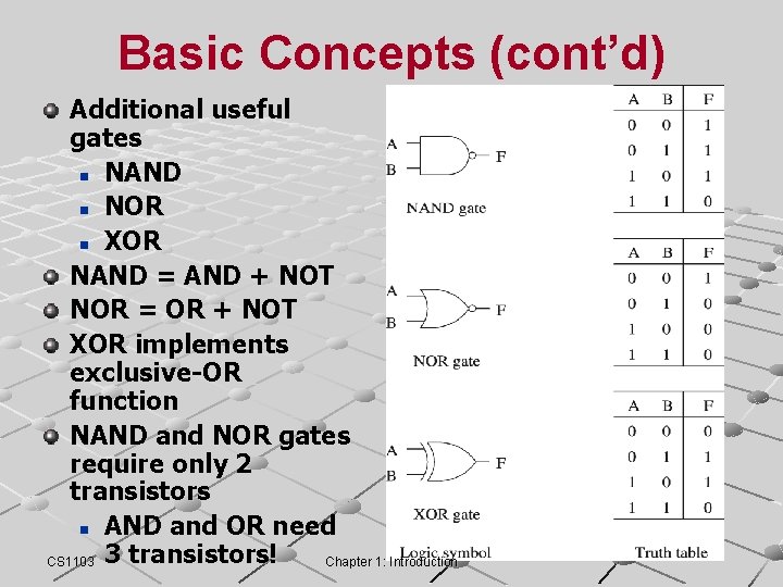
Basic Concepts (cont’d) Additional useful gates n NAND n NOR n XOR NAND = AND + NOT NOR = OR + NOT XOR implements exclusive-OR function NAND and NOR gates require only 2 transistors n AND and OR need CS 1103 3 transistors! Chapter 1: Introduction
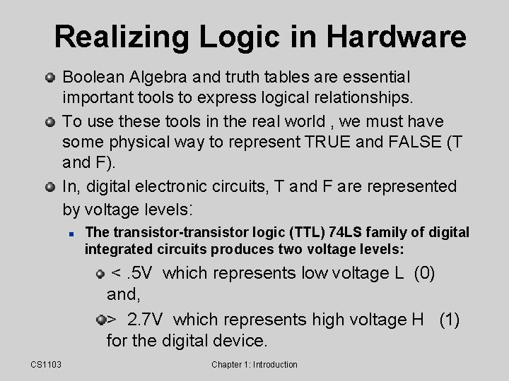
Realizing Logic in Hardware Boolean Algebra and truth tables are essential important tools to express logical relationships. To use these tools in the real world , we must have some physical way to represent TRUE and FALSE (T and F). In, digital electronic circuits, T and F are represented by voltage levels: n The transistor-transistor logic (TTL) 74 LS family of digital integrated circuits produces two voltage levels: <. 5 V which represents low voltage L (0) and, > 2. 7 V which represents high voltage H (1) for the digital device. CS 1103 Chapter 1: Introduction
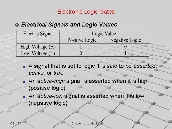
Electronic Logic Gates Electrical Signals and Logic Values n n n CS 1103 A signal that is set to logic 1 is said to be asserted, active, or true. An active-high signal is asserted when it is high (positive logic). An active-low signal is asserted when it is low (negative logic). Chapter 1: Introduction
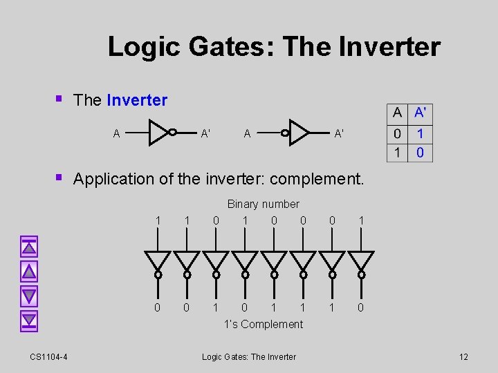
Logic Gates: The Inverter § The Inverter A A' § Application of the inverter: complement. CS 1104 -4 1 1 Binary number 0 1 0 1 1 1’s Complement Logic Gates: The Inverter 0 1 1 0 12
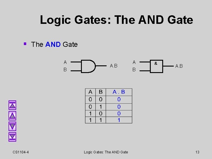
Logic Gates: The AND Gate § The AND Gate A B CS 1104 -4 A. B Logic Gates: The AND Gate A B & A. B 13
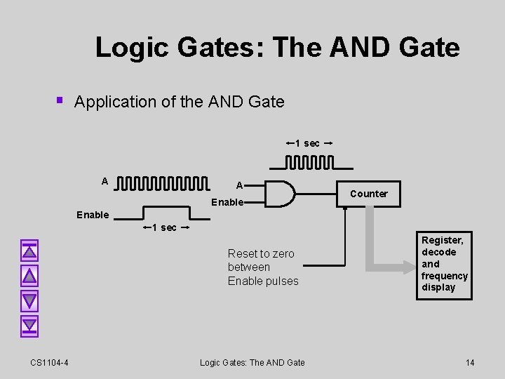
Logic Gates: The AND Gate § Application of the AND Gate 1 sec A A Enable Counter Enable 1 sec Reset to zero between Enable pulses CS 1104 -4 Logic Gates: The AND Gate Register, decode and frequency display 14
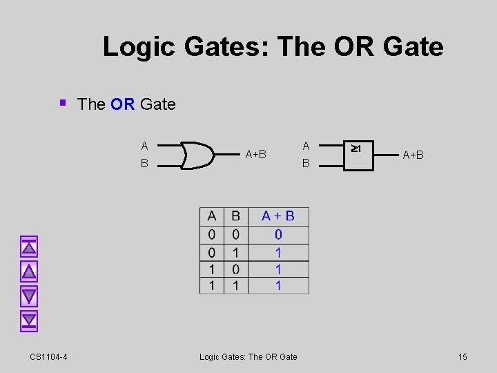
Logic Gates: The OR Gate § The OR Gate A B CS 1104 -4 A+B Logic Gates: The OR Gate A B 1 A+B 15
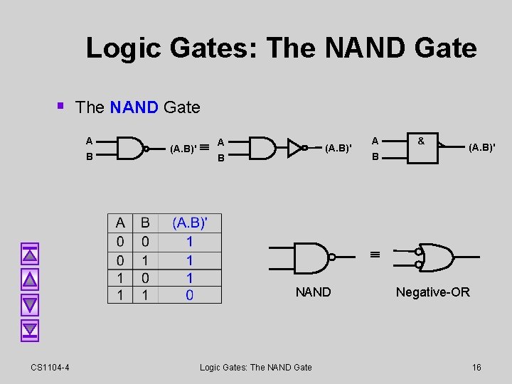
Logic Gates: The NAND Gate § The NAND Gate A B (A. B)' A (A. B)' B A B & (A. B)' NAND CS 1104 -4 Logic Gates: The NAND Gate Negative-OR 16
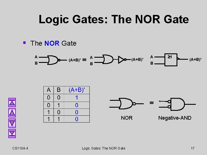
Logic Gates: The NOR Gate § The NOR Gate A B (A+B)' A (A+B)' B A B 1 (A+B)' NOR CS 1104 -4 Logic Gates: The NOR Gate Negative-AND 17
Logic Gates: The XOR Gate § The XOR Gate A B CS 1104 -4 A B Logic Gates: The XOR Gate A B =1 A B 18
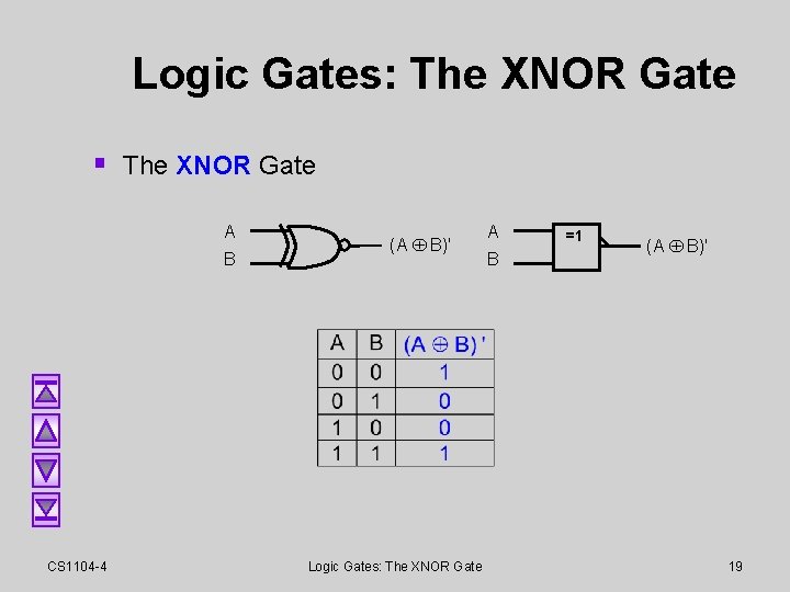
Logic Gates: The XNOR Gate § The XNOR Gate A B CS 1104 -4 (A B)' Logic Gates: The XNOR Gate A B =1 (A B)' 19
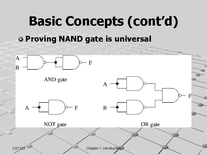
Basic Concepts (cont’d) Proving NAND gate is universal CS 1103 Chapter 1: Introduction
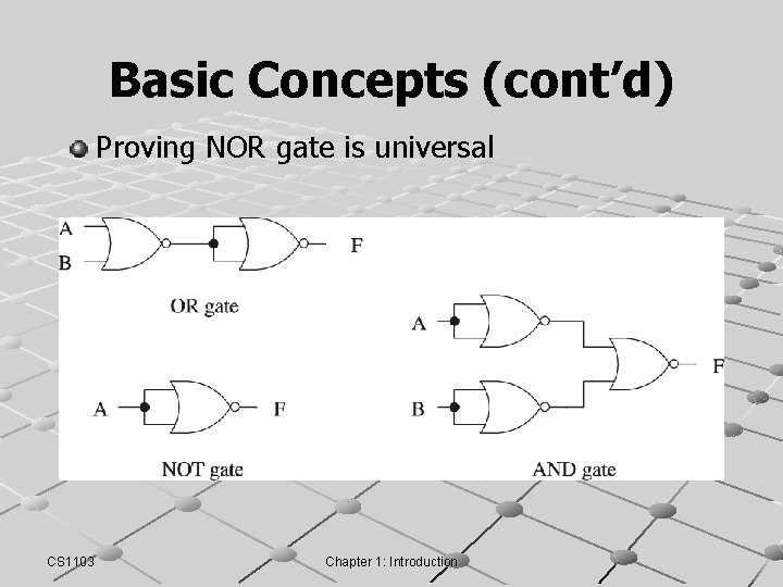
Basic Concepts (cont’d) Proving NOR gate is universal CS 1103 Chapter 1: Introduction
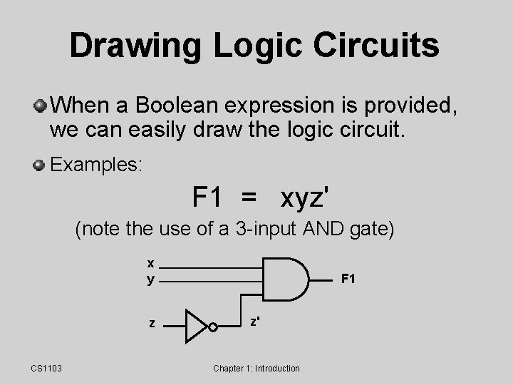
Drawing Logic Circuit § When a Boolean expression is provided, we can easily draw the logic circuit. § Examples: (i) F 1 = xyz' (note the use of a 3 -input AND gate) x y z CS 1104 -4 F 1 z' Drawing Logic Circuit 22
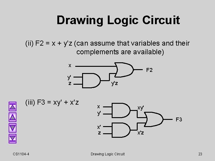
Drawing Logic Circuit (ii) F 2 = x + y'z (can assume that variables and their complements are available) x F 2 y' z (iii) F 3 = xy' + x'z y'z x y' xy' F 3 x' z CS 1104 -4 Drawing Logic Circuit x'z 23
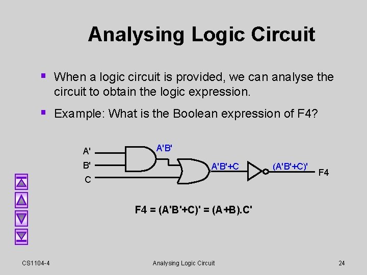
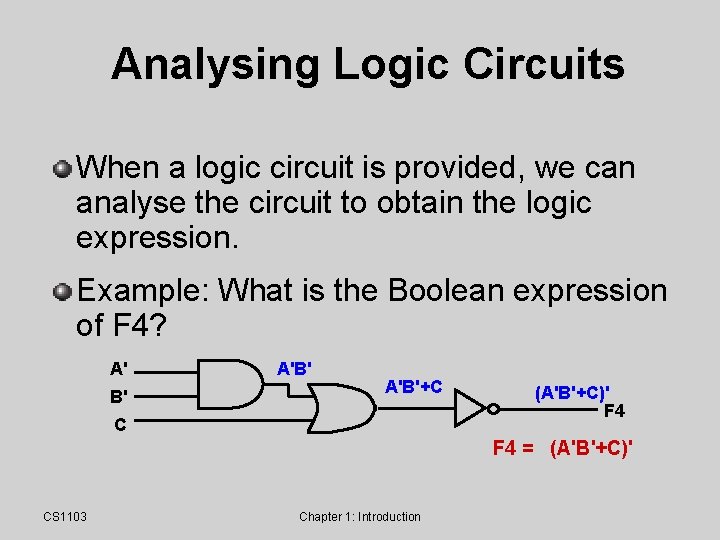
Analysing Logic Circuit § When a logic circuit is provided, we can analyse the circuit to obtain the logic expression. § Example: What is the Boolean expression of F 4? A' B' A'B'+C C (A'B'+C)' F 4 = (A'B'+C)' = (A+B). C' CS 1104 -4 Analysing Logic Circuit 24
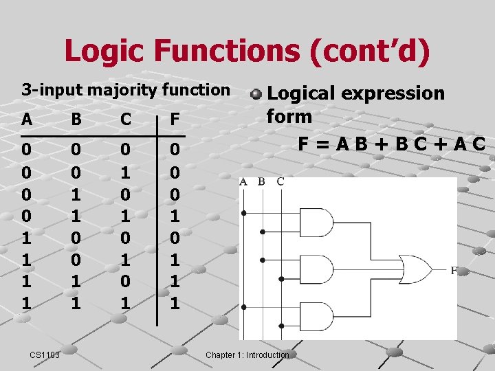
Logic Functions (cont’d) 3 -input majority function A B C F 0 0 1 1 0 1 0 1 0 0 0 1 1 1 CS 1103 Logical expression form F=AB+BC+AC Chapter 1: Introduction
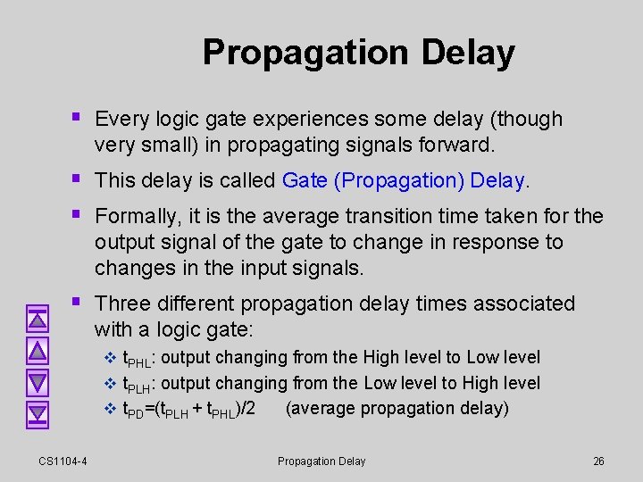
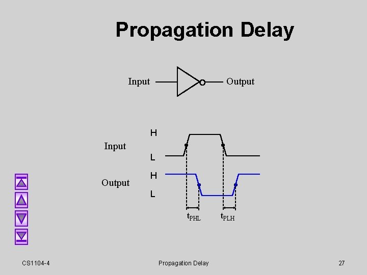
Propagation Delay § Every logic gate experiences some delay (though very small) in propagating signals forward. § This delay is called Gate (Propagation) Delay. § Formally, it is the average transition time taken for the output signal of the gate to change in response to changes in the input signals. § Three different propagation delay times associated with a logic gate: v t. PHL: output changing from the High level to Low level v t. PLH: output changing from the Low level to High level v t. PD=(t. PLH + t. PHL)/2 CS 1104 -4 (average propagation delay) Propagation Delay 26
Propagation Delay Input Output H Input L Output H L t. PHL CS 1104 -4 Propagation Delay t. PLH 27
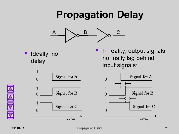
Propagation Delay A B C § In reality, output signals § Ideally, no normally lag behind input signals: delay: 1 0 1 0 1 Signal for A Signal for B Signal for C time CS 1104 -4 0 1 0 Signal for A Signal for B Signal for C time Propagation Delay 28
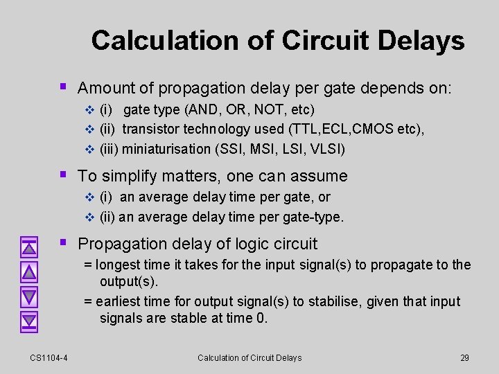
Calculation of Circuit Delays § Amount of propagation delay per gate depends on: v (i) gate type (AND, OR, NOT, etc) v (ii) transistor technology used (TTL, ECL, CMOS etc), v (iii) miniaturisation (SSI, MSI, LSI, VLSI) § To simplify matters, one can assume v (i) an average delay time per gate, or v (ii) an average delay time per gate-type. § Propagation delay of logic circuit = longest time it takes for the input signal(s) to propagate to the output(s). = earliest time for output signal(s) to stabilise, given that input signals are stable at time 0. CS 1104 -4 Calculation of Circuit Delays 29
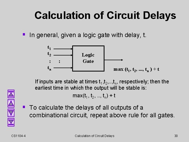
Calculation of Circuit Delays § In general, given a logic gate with delay, t. t 1 t 2 : tn : Logic Gate max (t 1, t 2, . . . , tn ) + t If inputs are stable at times t 1, t 2, . . , tn, respectively; then the earliest time in which the output will be stable is: max(t 1, t 2, . . , tn) + t § To calculate the delays of all outputs of a combinational circuit, repeat above rule for all gates. CS 1104 -4 Calculation of Circuit Delays 30
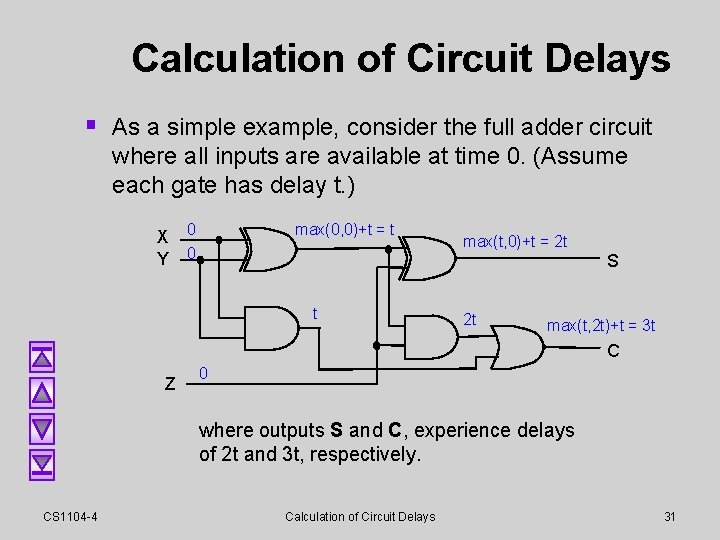
Calculation of Circuit Delays § As a simple example, consider the full adder circuit where all inputs are available at time 0. (Assume each gate has delay t. ) X Y max(0, 0)+t = t 0 0 max(t, 0)+t = 2 t S t 2 t max(t, 2 t)+t = 3 t C Z 0 where outputs S and C, experience delays of 2 t and 3 t, respectively. CS 1104 -4 Calculation of Circuit Delays 31
Universal Gates: NAND and NOR § AND/OR/NOT gates are sufficient for building any § Boolean functions. We call the set {AND, OR, NOT} a complete set of logic. § However, other gates are also used because: (i) usefulness (ii) economical on transistors (iii) self-sufficient NAND/NOR: economical, self-sufficient XOR: useful (e. g. parity bit generation) CS 1104 -4 Universal Gates: NAND and NOR 32
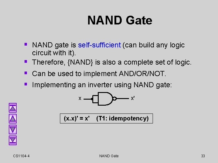
NAND Gate § NAND gate is self-sufficient (can build any logic circuit with it). Therefore, {NAND} is also a complete set of logic. § § Can be used to implement AND/OR/NOT. § Implementing an inverter using NAND gate: x (x. x)' = x' CS 1104 -4 x' (T 1: idempotency) NAND Gate 33
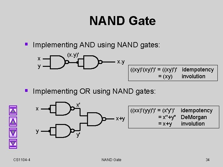
NAND Gate § Implementing AND using NAND gates: x y (x. y)' x. y ((xy)')' = ((xy)')' idempotency = (xy) involution § Implementing OR using NAND gates: x y CS 1104 -4 x' ((xx)'(yy)')' = (x'y')' idempotency = x''+y'' De. Morgan x+y = x+y involution y' NAND Gate 34
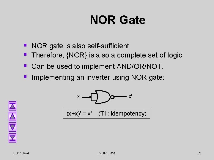
NOR Gate § § NOR gate is also self-sufficient. Therefore, {NOR} is also a complete set of logic Can be used to implement AND/OR/NOT. Implementing an inverter using NOR gate: x (x+x)' = x' CS 1104 -4 x' (T 1: idempotency) NOR Gate 35
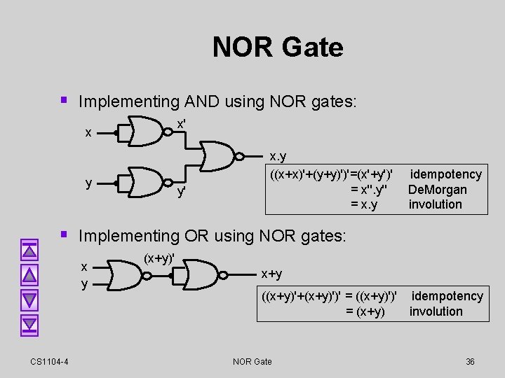
NOR Gate § Implementing AND using NOR gates: x' x y y' x. y ((x+x)'+(y+y)')'=(x'+y')' = x''. y'' = x. y idempotency De. Morgan involution § Implementing OR using NOR gates: x y CS 1104 -4 (x+y)' x+y ((x+y)'+(x+y)')' = ((x+y)')' idempotency = (x+y) involution NOR Gate 36
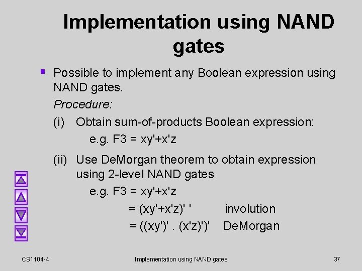
Implementation using NAND gates § Possible to implement any Boolean expression using NAND gates. Procedure: (i) Obtain sum-of-products Boolean expression: e. g. F 3 = xy'+x'z (ii) Use De. Morgan theorem to obtain expression using 2 -level NAND gates e. g. F 3 = xy'+x'z = (xy'+x'z)' ' involution = ((xy')'. (x'z)')' De. Morgan CS 1104 -4 Implementation using NAND gates 37
Implementation using NAND gates x y' (xy')' x' z (x'z)' F 3 = ((xy')'. (x'z)') ' = xy' + x'z CS 1104 -4 Implementation using NAND gates 38
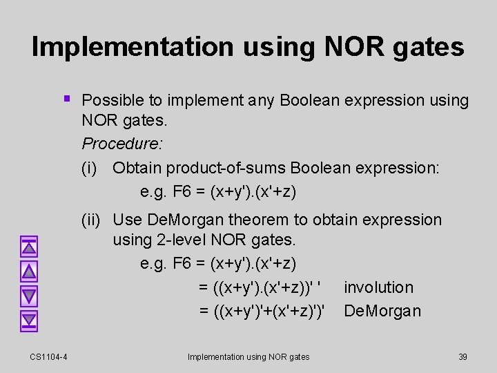
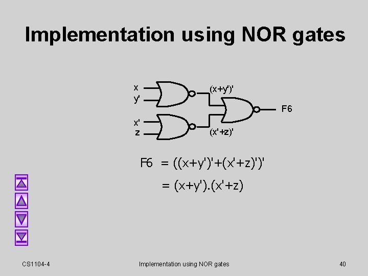
Implementation using NOR gates § Possible to implement any Boolean expression using NOR gates. Procedure: (i) Obtain product-of-sums Boolean expression: e. g. F 6 = (x+y'). (x'+z) (ii) Use De. Morgan theorem to obtain expression using 2 -level NOR gates. e. g. F 6 = (x+y'). (x'+z) = ((x+y'). (x'+z))' ' involution = ((x+y')'+(x'+z)')' De. Morgan CS 1104 -4 Implementation using NOR gates 39
Implementation using NOR gates x y' (x+y')' x' z (x'+z)' F 6 = ((x+y')'+(x'+z)')' = (x+y'). (x'+z) CS 1104 -4 Implementation using NOR gates 40
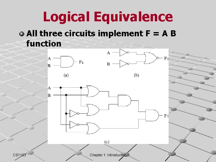
Logical Equivalence All three circuits implement F = A B function CS 1103 Chapter 1: Introduction
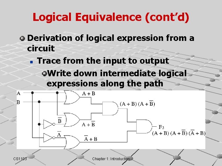
Logical Equivalence (cont’d) Derivation of logical expression from a circuit n Trace from the input to output Write down intermediate logical expressions along the path CS 1103 Chapter 1: Introduction
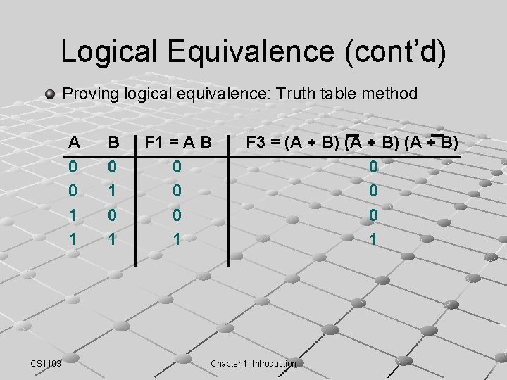
Logical Equivalence (cont’d) Proving logical equivalence: Truth table method A 0 0 1 1 CS 1103 B 0 1 F 1 = A B 0 0 0 1 F 3 = (A + B) 0 0 0 1 Chapter 1: Introduction
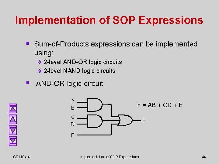
Implementation of SOP Expressions § Sum-of-Products expressions can be implemented using: v 2 -level AND-OR logic circuits v 2 -level NAND logic circuits § AND-OR logic circuit A B F = AB + CD + E C F D E CS 1104 -4 Implementation of SOP Expressions 44
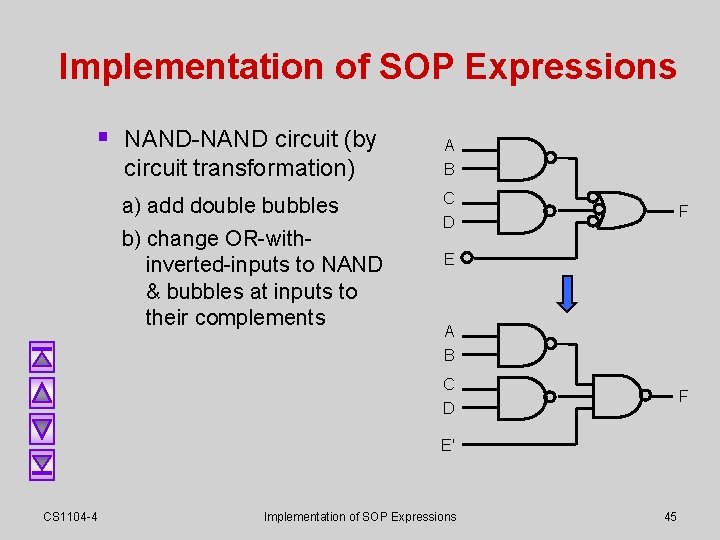
Implementation of SOP Expressions § NAND-NAND circuit (by circuit transformation) a) add double bubbles b) change OR-withinverted-inputs to NAND & bubbles at inputs to their complements A B C D F E A B C F D E' CS 1104 -4 Implementation of SOP Expressions 45
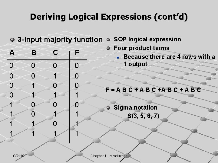
Deriving Logical Expressions (cont’d) 3 -input majority function A B C F 0 0 1 1 0 1 0 1 0 0 0 1 1 1 CS 1103 SOP logical expression Four product terms n Because there are 4 rows with a 1 output F = A B C +A B C + A B C Sigma notation S(3, 5, 6, 7) Chapter 1: Introduction
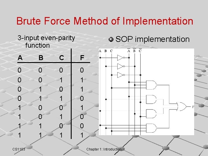
Brute Force Method of Implementation 3 -input even-parity function SOP implementation A B C F 0 0 1 1 0 1 0 1 0 1 1 0 0 1 CS 1103 Chapter 1: Introduction
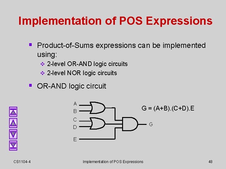
Implementation of POS Expressions § Product-of-Sums expressions can be implemented using: v 2 -level OR-AND logic circuits v 2 -level NOR logic circuits § OR-AND logic circuit A B G = (A+B). (C+D). E C D G E CS 1104 -4 Implementation of POS Expressions 48
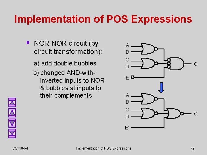
Implementation of POS Expressions § NOR-NOR circuit (by circuit transformation): a) add double bubbles b) changed AND-withinverted-inputs to NOR & bubbles at inputs to their complements A B C D G E' CS 1104 -4 Implementation of POS Expressions 49
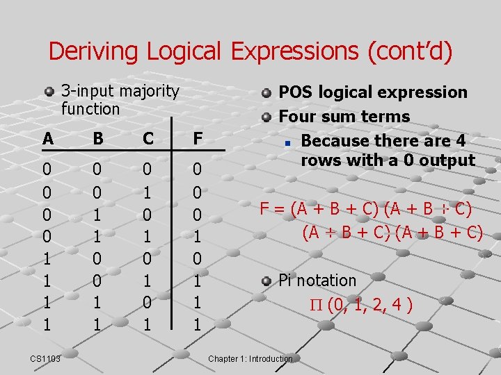
Deriving Logical Expressions (cont’d) 3 -input majority function A B C F 0 0 1 1 0 1 0 1 0 0 0 1 1 1 CS 1103 POS logical expression Four sum terms n Because there are 4 rows with a 0 output F = (A + B + C) Pi notation (0, 1, 2, 4 ) Chapter 1: Introduction
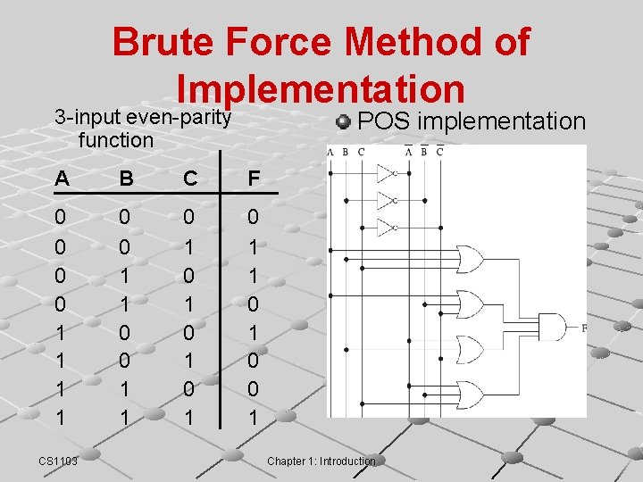
Brute Force Method of Implementation 3 -input even-parity function POS implementation A B C F 0 0 1 1 0 1 0 1 0 1 1 0 0 1 CS 1103 Chapter 1: Introduction
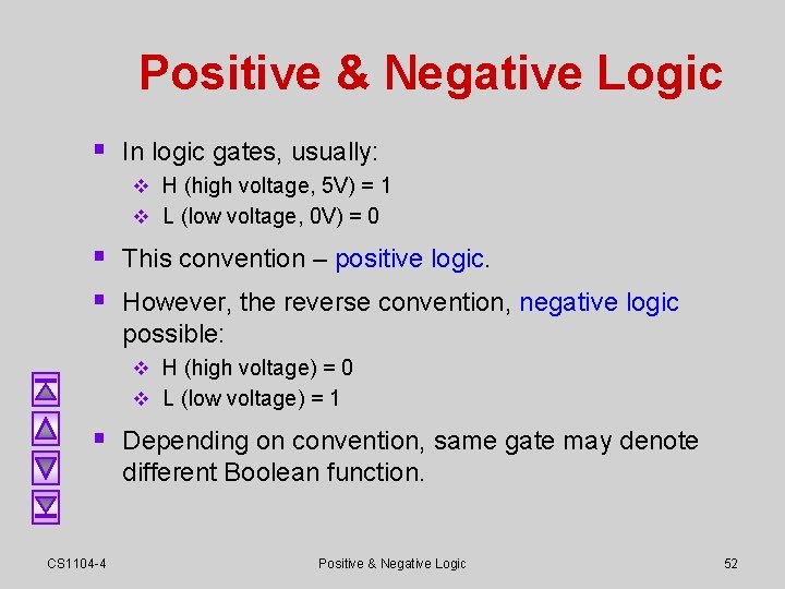
Positive & Negative Logic § In logic gates, usually: v H (high voltage, 5 V) = 1 v L (low voltage, 0 V) = 0 § This convention – positive logic. § However, the reverse convention, negative logic possible: v H (high voltage) = 0 v L (low voltage) = 1 § Depending on convention, same gate may denote different Boolean function. CS 1104 -4 Positive & Negative Logic 52
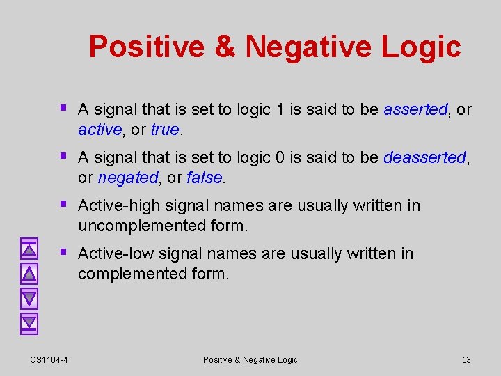
Positive & Negative Logic § A signal that is set to logic 1 is said to be asserted, or active, or true. § A signal that is set to logic 0 is said to be deasserted, or negated, or false. § Active-high signal names are usually written in uncomplemented form. § Active-low signal names are usually written in complemented form. CS 1104 -4 Positive & Negative Logic 53
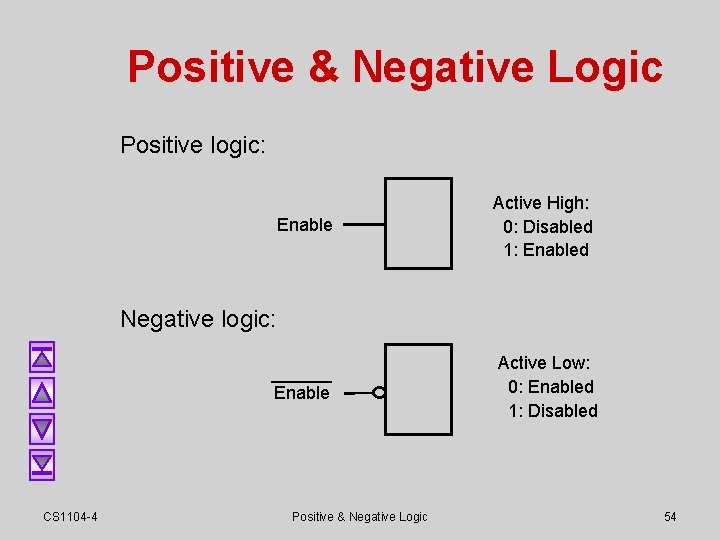
Positive & Negative Logic Positive logic: Enable Active High: 0: Disabled 1: Enabled Negative logic: Enable CS 1104 -4 Positive & Negative Logic Active Low: 0: Enabled 1: Disabled 54
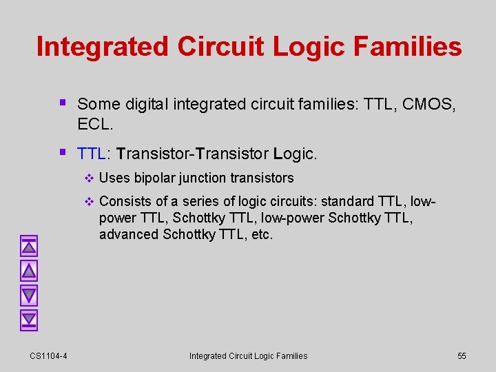
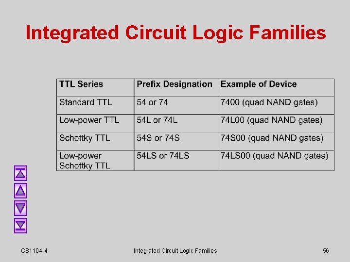
Integrated Circuit Logic Families § Some digital integrated circuit families: TTL, CMOS, ECL. § TTL: Transistor-Transistor Logic. v Uses bipolar junction transistors v Consists of a series of logic circuits: standard TTL, low- power TTL, Schottky TTL, low-power Schottky TTL, advanced Schottky TTL, etc. CS 1104 -4 Integrated Circuit Logic Families 55
Integrated Circuit Logic Families CS 1104 -4 Integrated Circuit Logic Families 56
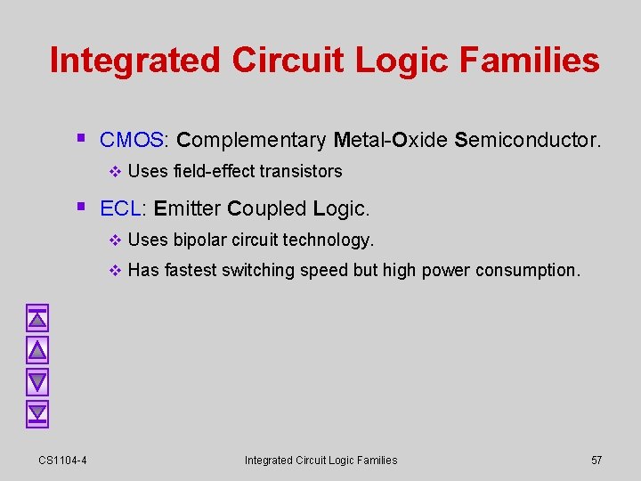
Integrated Circuit Logic Families § CMOS: Complementary Metal-Oxide Semiconductor. v Uses field-effect transistors § ECL: Emitter Coupled Logic. v Uses bipolar circuit technology. v Has fastest switching speed but high power consumption. CS 1104 -4 Integrated Circuit Logic Families 57
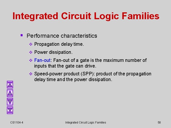
Integrated Circuit Logic Families § Performance characteristics v Propagation delay time. v Power dissipation. v Fan-out: Fan-out of a gate is the maximum number of inputs that the gate can drive. v Speed-power product (SPP): product of the propagation delay time and the power dissipation. CS 1104 -4 Integrated Circuit Logic Families 58
Drawing Logic Circuits When a Boolean expression is provided, we can easily draw the logic circuit. Examples: F 1 = xyz' (note the use of a 3 -input AND gate) x y z CS 1103 F 1 z' Chapter 1: Introduction
Analysing Logic Circuits When a logic circuit is provided, we can analyse the circuit to obtain the logic expression. Example: What is the Boolean expression of F 4? A' B' A'B'+C C (A'B'+C)' F 4 = (A'B'+C)' CS 1103 Chapter 1: Introduction
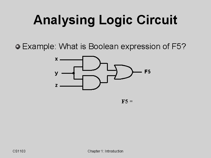
Analysing Logic Circuit Example: What is Boolean expression of F 5? x F 5 y z F 5 = CS 1103 Chapter 1: Introduction
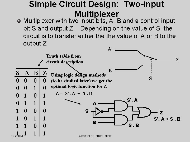
Simple Circuit Design: Two-input Multiplexer with two input bits, A, B and a control input bit S and output Z. Depending on the value of S, the circuit is to transfer either the value of A or B to the output Z A Truth table from circuit description S A 0 0 0 1 0 1 1 1 1 CS 1103 B 0 1 0 1 Z 0 0 1 1 0 1 Z B Using logic design methods (to be studied later) we get the optimal logic function for Z Z = S’. A + S. B A S S’. A S B Chapter 1: Introduction Z S’. A + S. B
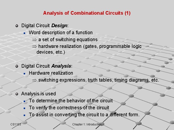
Analysis of Combinational Circuits (1) Digital Circuit Design: n Word description of a function a set of switching equations hardware realization (gates, programmable logic devices, etc. ) Digital Circuit Analysis: n Hardware realization switching expressions, truth tables, timing diagrams, etc. Analysis is used n To determine the behavior of the circuit n To verify the correctness of the circuit n To assist in converting the circuit to a different form. CS 1103 Chapter 1: Introduction
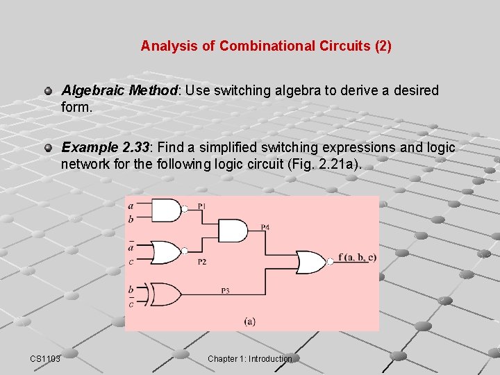
Analysis of Combinational Circuits (2) Algebraic Method: Use switching algebra to derive a desired form. Example 2. 33: Find a simplified switching expressions and logic network for the following logic circuit (Fig. 2. 21 a). CS 1103 Chapter 1: Introduction
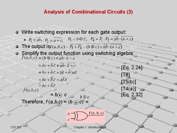
Analysis of Combinational Circuits (3) Write switching expression for each gate output: n The output is: Simplify the output function using switching algebra: =b c Therefore, f (a, b, c) = (b CS 1103 [Eq. 2. 24] [T 8] [T 5(b)] [T 4(a)] [Eq. 2. 32] c)' = Chapter 1: Introduction
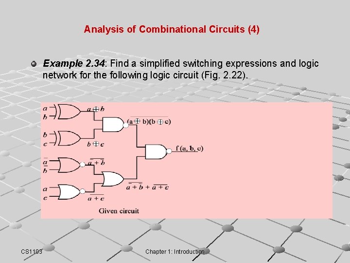
Analysis of Combinational Circuits (4) Example 2. 34: Find a simplified switching expressions and logic network for the following logic circuit (Fig. 2. 22). CS 1103 Chapter 1: Introduction
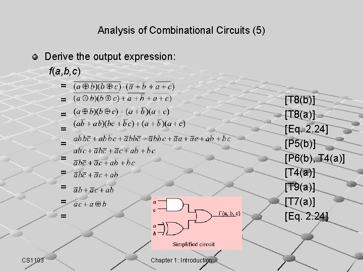
Analysis of Combinational Circuits (5) Derive the output expression: f(a, b, c) = = = = = CS 1103 Chapter 1: Introduction [T 8(b)] [T 8(a)] [Eq. 2. 24] [P 5(b)] [P 6(b), T 4(a)] [T 9(a)] [T 7(a)] [Eq. 2. 24]
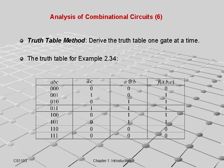
Analysis of Combinational Circuits (6) Truth Table Method: Derive the truth table one gate at a time. The truth table for Example 2. 34: CS 1103 Chapter 1: Introduction
Analysis of Combinational Circuits (7) Analysis of Timing Diagrams n Timing diagram is a graphical representation of input and output signal relationships over the time dimension. n Timing diagrams may show intermediate signals and propagation delays. CS 1103 Chapter 1: Introduction
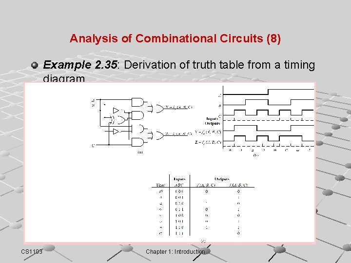
Analysis of Combinational Circuits (8) Example 2. 35: Derivation of truth table from a timing diagram CS 1103 Chapter 1: Introduction
CS 1103 Chapter 1: Introduction
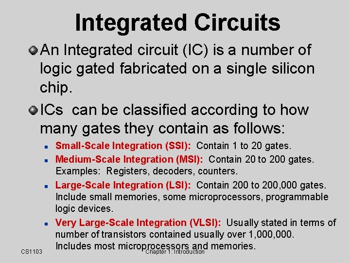
Integrated Circuits An Integrated circuit (IC) is a number of logic gated fabricated on a single silicon chip. ICs can be classified according to how many gates they contain as follows: n n CS 1103 Small-Scale Integration (SSI): Contain 1 to 20 gates. Medium-Scale Integration (MSI): Contain 20 to 200 gates. Examples: Registers, decoders, counters. Large-Scale Integration (LSI): Contain 200 to 200, 000 gates. Include small memories, some microprocessors, programmable logic devices. Very Large-Scale Integration (VLSI): Usually stated in terms of number of transistors contained usually over 1, 000. Includes most microprocessors and memories. Chapter 1: Introduction
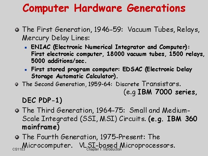
Computer Hardware Generations The First Generation, 1946 -59: Vacuum Tubes, Relays, Mercury Delay Lines: ENIAC (Electronic Numerical Integrator and Computer): First electronic computer, 18000 vacuum tubes, 1500 relays, 5000 additions/sec. n First stored program computer: EDSAC (Electronic Delay Storage Automatic Calculator). The Second Generation, 1959 -64: Discrete Transistors. n (e. g IBM 7000 series, DEC PDP-1) The Third Generation, 1964 -75: Small and Medium. Scale Integrated (SSI, MSI) Circuits. (e. g. IBM 360 mainframe) The Fourth Generation, 1975 -Present: The Microcomputer. VLSI-based Microprocessors. CS 1103 Chapter 1: Introduction
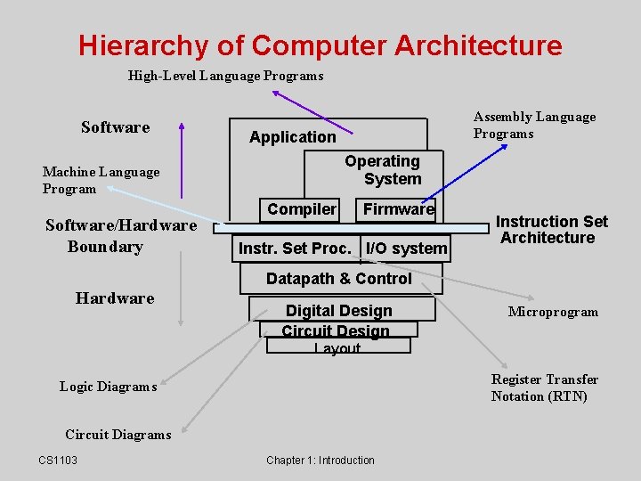
Hierarchy of Computer Architecture High-Level Language Programs Software Application Operating System Machine Language Program Software/Hardware Boundary Assembly Language Programs Compiler Firmware Instr. Set Proc. I/O system Instruction Set Architecture Datapath & Control Hardware Digital Design Circuit Design Microprogram Layout Register Transfer Notation (RTN) Logic Diagrams Circuit Diagrams CS 1103 Chapter 1: Introduction
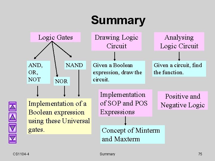
Summary Logic Gates AND, OR, NOT NAND NOR Implementation of a Boolean expression using these Universal gates. CS 1104 -4 Drawing Logic Circuit Analysing Logic Circuit Given a Boolean expression, draw the circuit. Given a circuit, find the function. Implementation of SOP and POS Expressions Positive and Negative Logic Concept of Minterm and Maxterm Summary 75
End of file