Unit 2 Logic Gates And Logic Families 1


- Slides: 43

Unit 2 Logic Gates And Logic Families 1

3 Types of Basic Gates 1. NOT Gate 1. Symbol 2. Truth Table 3. Expression 2. AND Gate 3. OR Gate 2

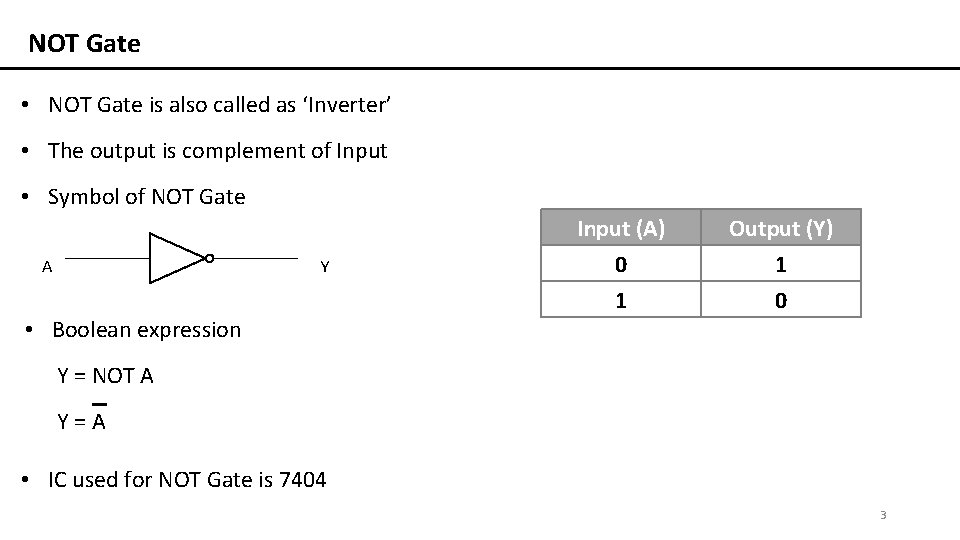
NOT Gate • NOT Gate is also called as ‘Inverter’ • The output is complement of Input • Symbol of NOT Gate A Y • Boolean expression Input (A) 0 1 Output (Y) 1 0 Y = NOT A Y=A • IC used for NOT Gate is 7404 3

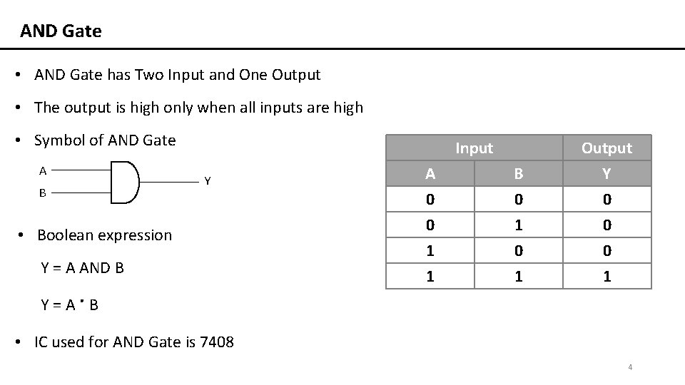
AND Gate • AND Gate has Two Input and One Output • The output is high only when all inputs are high • Symbol of AND Gate A B Input Y • Boolean expression Y = A AND B A 0 0 B 0 1 Output Y 0 0 1 1 0 1 Y=A·B • IC used for AND Gate is 7408 4

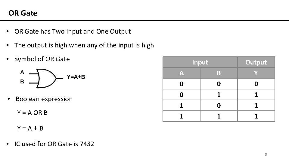
OR Gate • OR Gate has Two Input and One Output • The output is high when any of the input is high • Symbol of OR Gate • Boolean expression Y = A OR B Input A 0 0 B 0 1 Output Y 0 1 1 1 Y=A+B • IC used for OR Gate is 7432 5

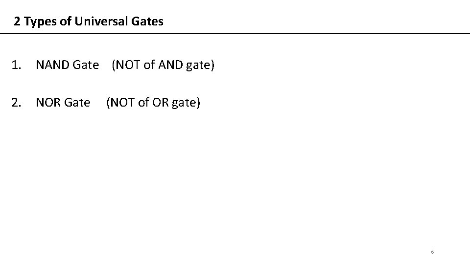
2 Types of Universal Gates 1. NAND Gate (NOT of AND gate) 2. NOR Gate (NOT of OR gate) 6

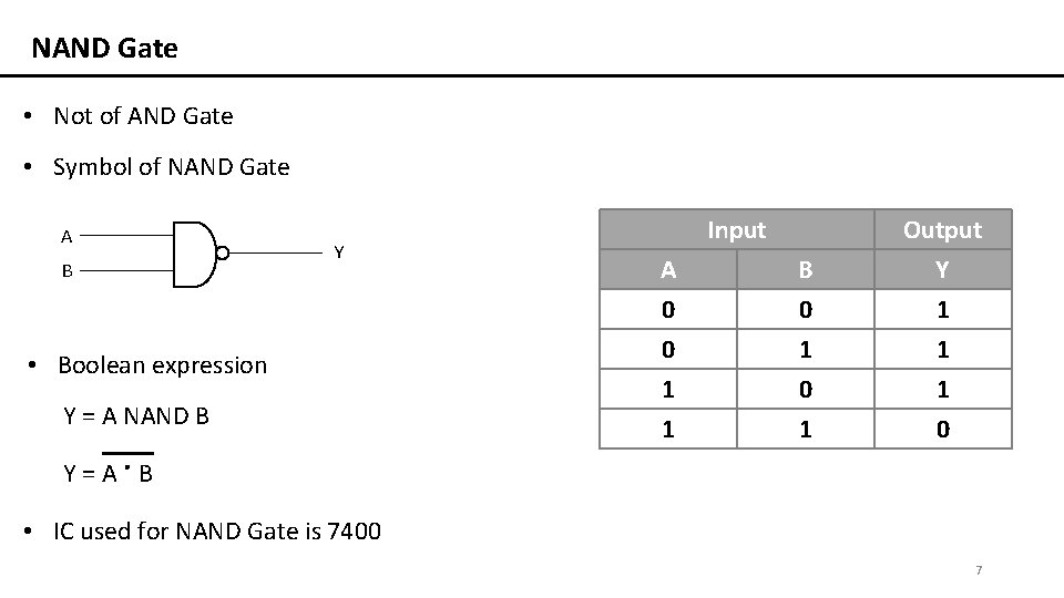
NAND Gate • Not of AND Gate • Symbol of NAND Gate A B Y • Boolean expression Y = A NAND B Input A 0 0 B 0 1 Output Y 1 1 0 Y=A·B • IC used for NAND Gate is 7400 7

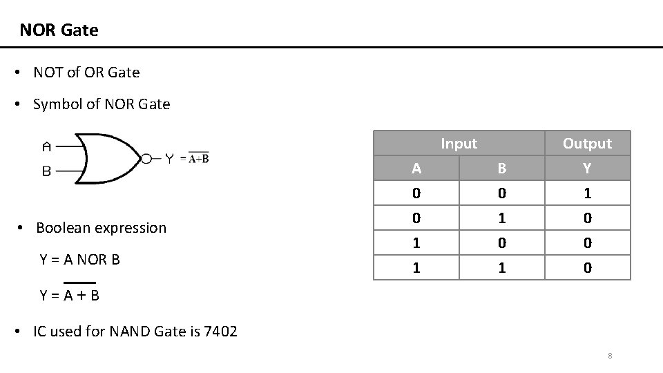
NOR Gate • NOT of OR Gate • Symbol of NOR Gate Input • Boolean expression Y = A NOR B A 0 0 B 0 1 Output Y 1 0 1 0 0 Y=A+B • IC used for NAND Gate is 7402 8

Universal Gate • NAND and NOR Gate are called as Universal Gate, because these both Gates can be used alone to generate remaining Gate, such as NOT, AND, OR Gate • So by using only NAND or NOR Gate we can implement logic circuits. Thus NAND and NOR Gates are called as the Universal Gate

2 Types of Special Gates 1. Exclusive OR Gate ( Ex – OR) NOT 2. Exclusive NOR Gate ( Ex – NOR) 10

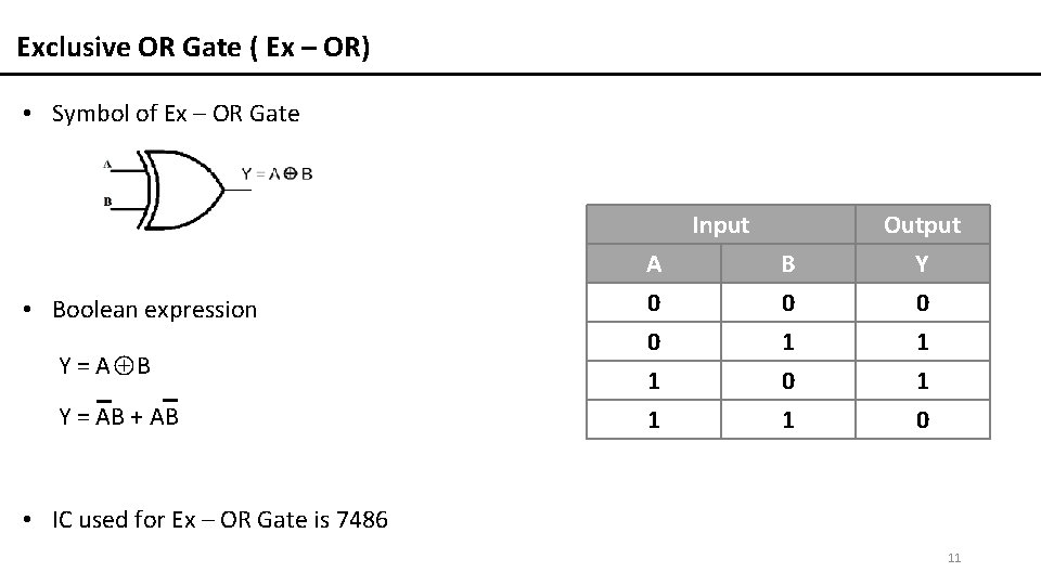
Exclusive OR Gate ( Ex – OR) • Symbol of Ex – OR Gate Input • Boolean expression Y=A B Y = AB + AB A 0 0 B 0 1 Output Y 0 1 1 1 0 • IC used for Ex – OR Gate is 7486 11

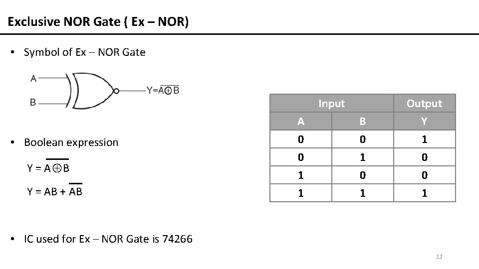
Exclusive NOR Gate ( Ex – NOR) • Symbol of Ex – NOR Gate Input • Boolean expression Y=A B Y = AB + AB A 0 0 B 0 1 Output Y 1 0 1 0 1 • IC used for Ex – NOR Gate is 74266 12

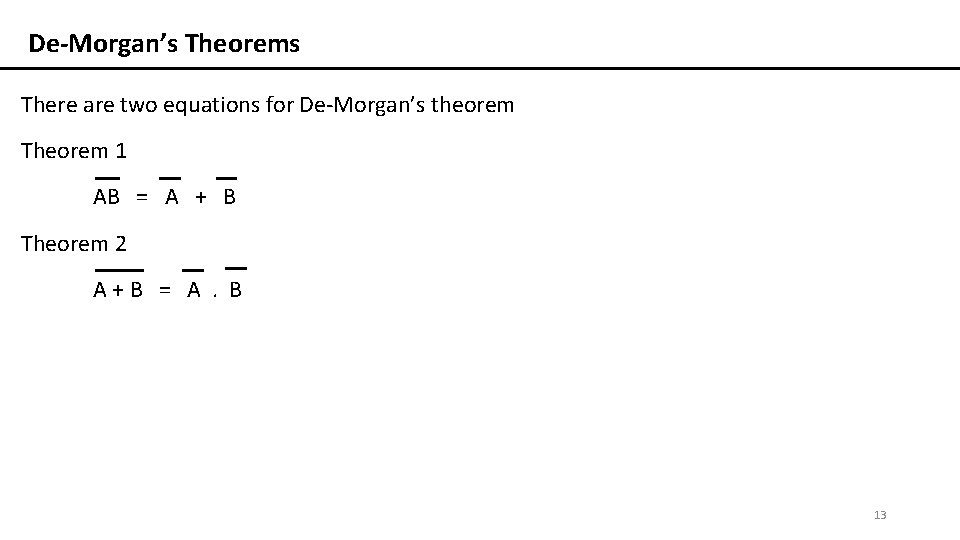
De-Morgan’s Theorems There are two equations for De-Morgan’s theorem Theorem 1 AB = A + B Theorem 2 A+B = A. B 13

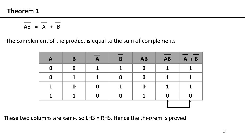
Theorem 1 AB = A + B The complement of the product is equal to the sum of complements A B AB AB A +B 0 0 1 1 1 0 0 0 1 1 1 0 These two columns are same, so LHS = RHS. Hence theorem is proved. 14

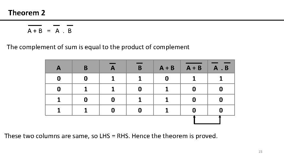
Theorem 2 A+B = A. B The complement of sum is equal to the product of complement A B A+B A. B 0 0 1 1 1 0 0 0 1 1 1 0 0 0 These two columns are same, so LHS = RHS. Hence theorem is proved. 15

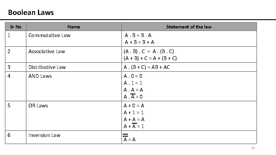
Boolean Laws Sr No Name Statement of the law 1 Commutative Law A. B=B. A A+B=B+A 2 Associative Law (A. B). C = A. (B. C) (A + B) + C = A + (B + C) 3 Distributive Law A. (B + C) = AB + AC 4 AND Laws A. 0=0 A. 1=1 A. A=A A. A=0 5 OR Laws A+0=A A+1=1 A+A=A A+A=1 6 Inversion Law A=A 16

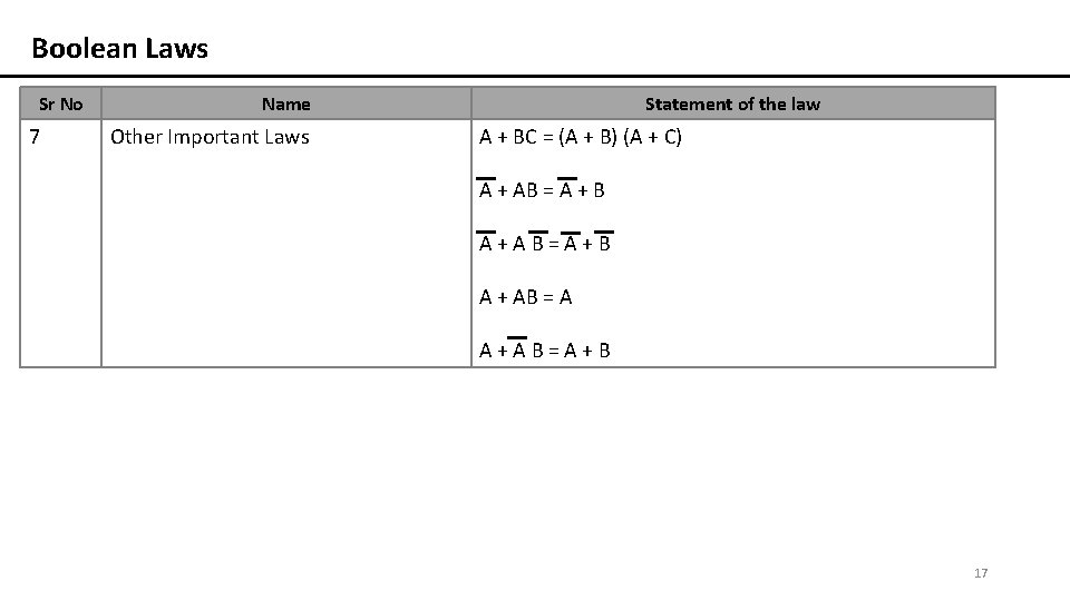
Boolean Laws Sr No 7 Name Other Important Laws Statement of the law A + BC = (A + B) (A + C) A + AB = A + B A+AB=A+B A + AB = A A+AB=A+B 17

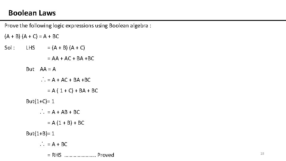
Boolean Laws Prove the following logic expressions using Boolean algebra : (A + B) (A + C) = A + BC Sol : LHS = (A + B) (A + C) = AA + AC + BA +BC But AA = A. . . = A + AC + BA +BC = A ( 1 + C) + BA + BC But(1+C)= 1. . . = A + AB + BC = A (1 + B) + BC But(1+B)= 1. . . = A + BC = RHS …………………. . Proved 18

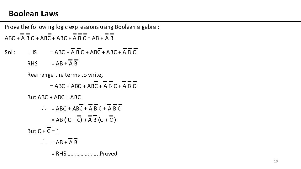
Boolean Laws Prove the following logic expressions using Boolean algebra : ABC + A B C + ABC + A B C = AB + A B Sol : LHS = ABC + A B C + ABC + A B C RHS = AB + A B Rearrange the terms to write, = ABC + A B C But ABC + ABC = ABC . . . = ABC + A B C = AB ( C + C) + A B (C + C ) But C + C = 1 . . . = AB + A B = RHS…………………. . Proved 19

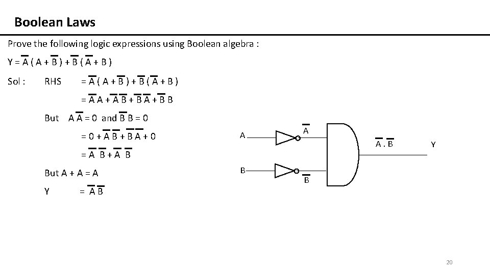
Boolean Laws Prove the following logic expressions using Boolean algebra : Y=A(A+B)+B(A+B) Sol : RHS =A(A+B)+B(A+B) =AA+AB+BA+BB But A A = 0 and B B = 0 =0+AB+BA+0 A A A. B =A B+A B But A + A = A Y = AB B Y B 20

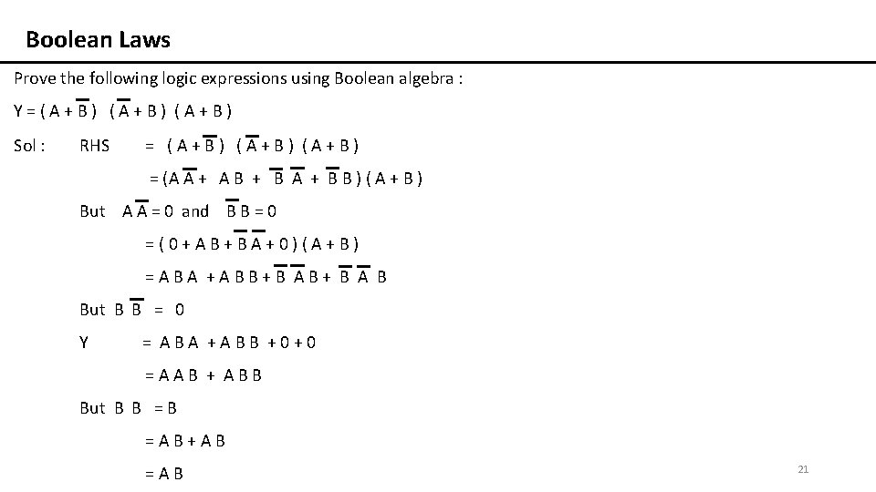
Boolean Laws Prove the following logic expressions using Boolean algebra : Y=(A+B) Sol : RHS = (A+B) = (A A + A B + B A + B B ) ( A + B ) But A A = 0 and B B = 0 =(0+AB+BA+0)(A+B) =ABA +ABB+B AB+ B A B But B B = 0 Y = ABA +ABB +0+0 =AAB + ABB But B B =AB+AB =AB 21

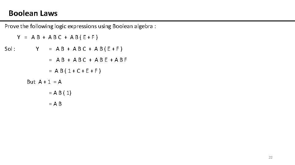
Boolean Laws Prove the following logic expressions using Boolean algebra : Y = AB + ABC + AB(E+F) Sol : Y = AB + ABC + AB(E+F) = AB + ABC + ABE +ABF = AB(1+C+E+F) But A + 1 = A B ( 1) =AB 22

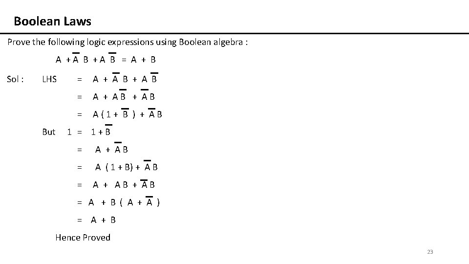
Boolean Laws Prove the following logic expressions using Boolean algebra : A +A B = A + B Sol : LHS But = A + A B = A + AB = A(1+ B ) + AB 1 = 1+B = A + AB = A ( 1 + B) + A B = A + AB = A + B ( A + A ) = A + B Hence Proved 23

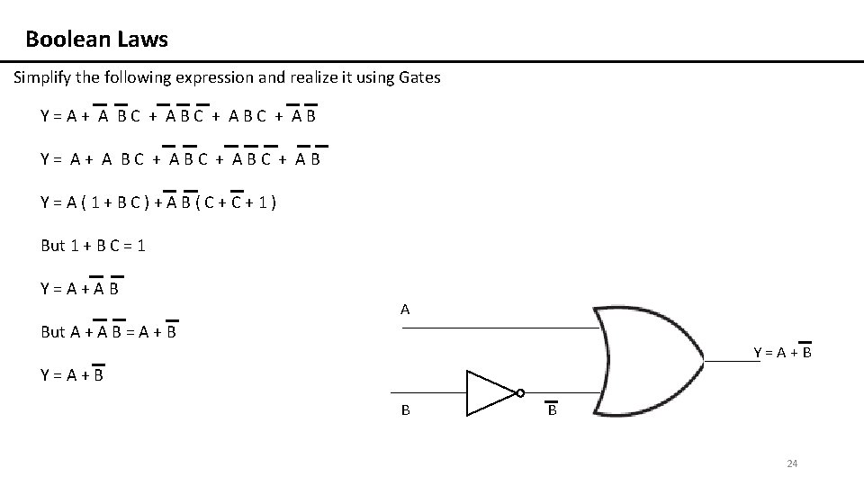
Boolean Laws Simplify the following expression and realize it using Gates Y=A+ A BC + ABC + AB Y=A(1+BC)+AB(C+C+1) But 1 + B C = 1 Y=A+AB A But A + A B = A + B Y=A+B B B 24

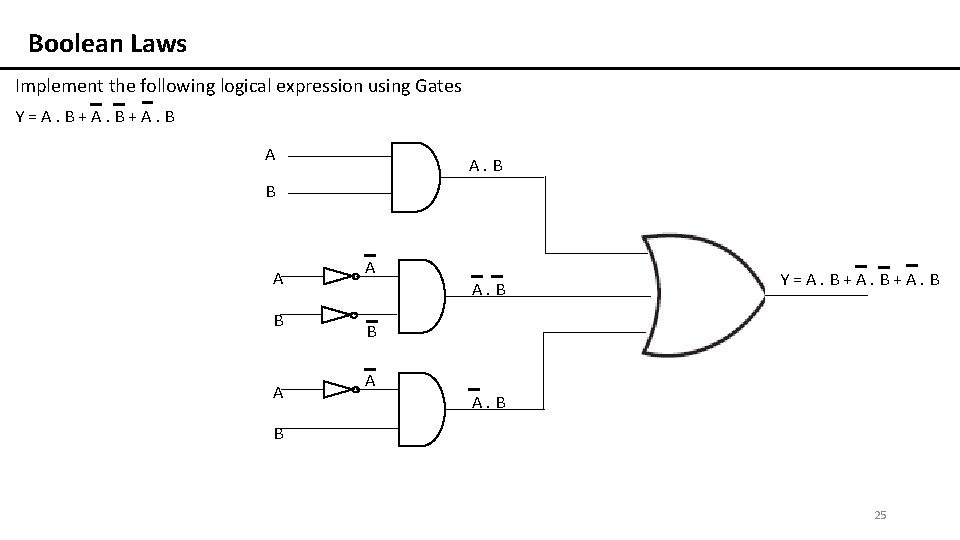
Boolean Laws Implement the following logical expression using Gates Y=A. B+A. B A A. B B A A A. B Y=A. B+A. B B A A. B B 25

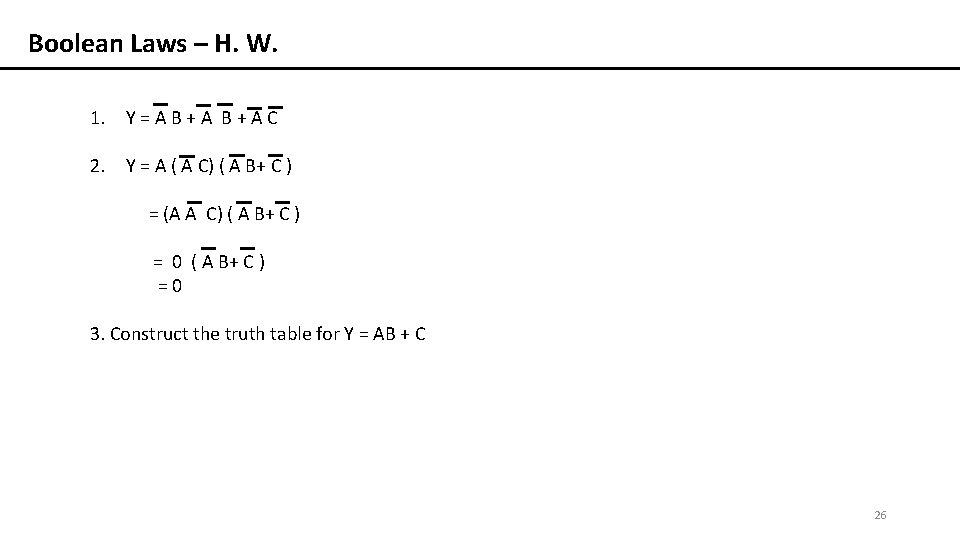
Boolean Laws – H. W. 1. Y = A B + A C 2. Y = A ( A C) ( A B+ C ) = (A A C) ( A B+ C ) = 0 ( A B+ C ) =0 3. Construct the truth table for Y = AB + C 26

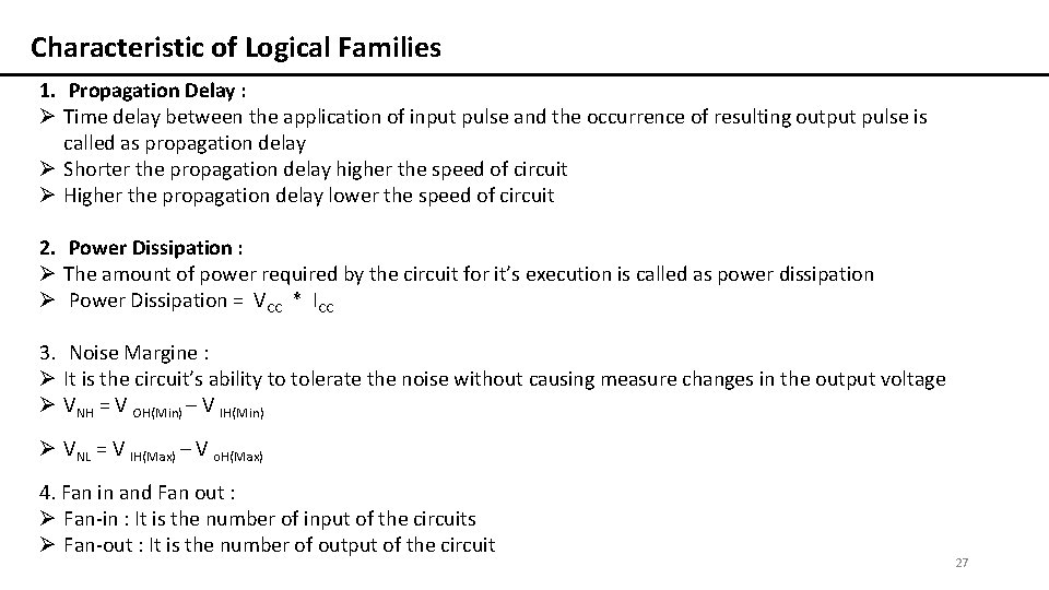
Characteristic of Logical Families 1. Propagation Delay : Ø Time delay between the application of input pulse and the occurrence of resulting output pulse is called as propagation delay Ø Shorter the propagation delay higher the speed of circuit Ø Higher the propagation delay lower the speed of circuit 2. Power Dissipation : Ø The amount of power required by the circuit for it’s execution is called as power dissipation Ø Power Dissipation = VCC * ICC 3. Noise Margine : Ø It is the circuit’s ability to tolerate the noise without causing measure changes in the output voltage Ø VNH = V OH(Min) – V IH(Min) Ø VNL = V IH(Max) – V o. H(Max) 4. Fan in and Fan out : Ø Fan-in : It is the number of input of the circuits Ø Fan-out : It is the number of output of the circuit 27

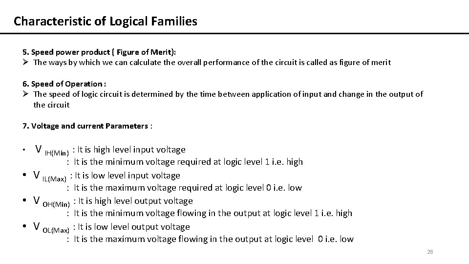
Characteristic of Logical Families 5. Speed power product ( Figure of Merit): Ø The ways by which we can calculate the overall performance of the circuit is called as figure of merit 6. Speed of Operation : Ø The speed of logic circuit is determined by the time between application of input and change in the output of the circuit 7. Voltage and current Parameters : • • V IH(Min) : It is high level input voltage : It is the minimum voltage required at logic level 1 i. e. high V IL(Max) : It is low level input voltage : It is the maximum voltage required at logic level 0 i. e. low V OH(Min) : It is high level output voltage : It is the minimum voltage flowing in the output at logic level 1 i. e. high V OL(Max) : It is low level output voltage : It is the maximum voltage flowing in the output at logic level 0 i. e. low 28

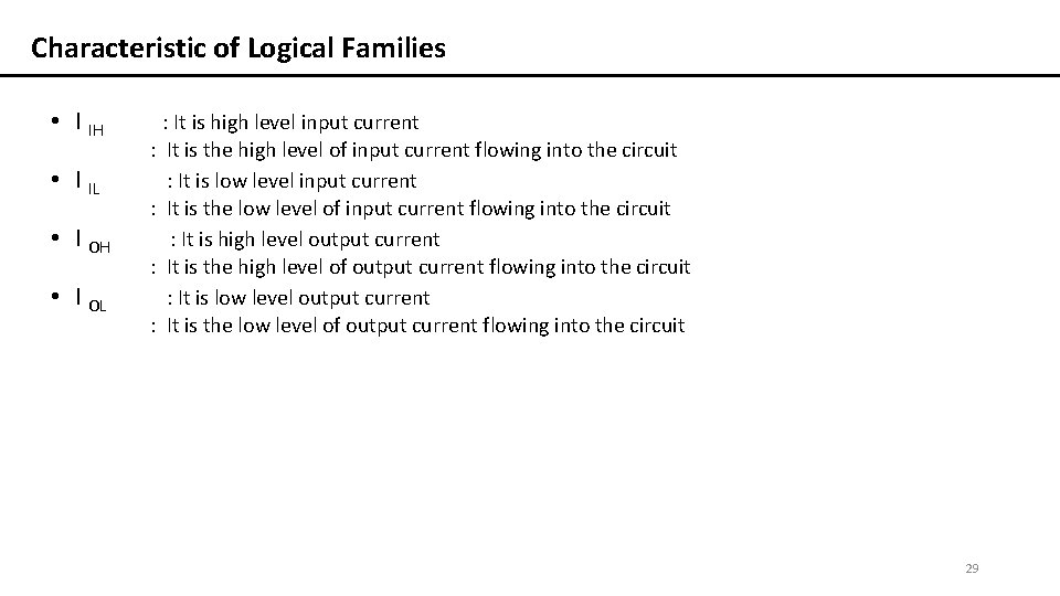
Characteristic of Logical Families • I IH • I IL • I OH • I OL : It is high level input current : It is the high level of input current flowing into the circuit : It is low level input current : It is the low level of input current flowing into the circuit : It is high level output current : It is the high level of output current flowing into the circuit : It is low level output current : It is the low level of output current flowing into the circuit 29

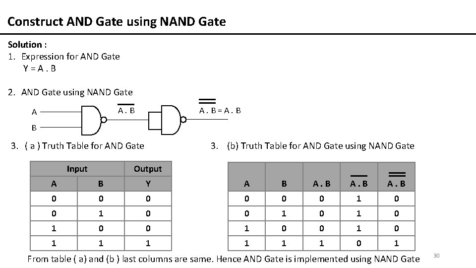
Construct AND Gate using NAND Gate Solution : 1. Expression for AND Gate Y=A. B 2. AND Gate using NAND Gate A. B A A. B=A. B B 3. ( a ) Truth Table for AND Gate Input 3. (b) Truth Table for AND Gate using NAND Gate Output A B Y A B A. B 0 0 0 1 0 1 0 1 1 1 0 1 From table ( a) and (b ) last columns are same. Hence AND Gate is implemented using NAND Gate 30

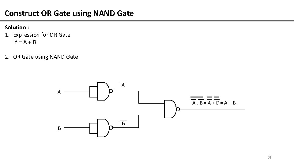
Construct OR Gate using NAND Gate Solution : 1. Expression for OR Gate Y=A+B 2. OR Gate using NAND Gate A A A. B=A+B B B 31

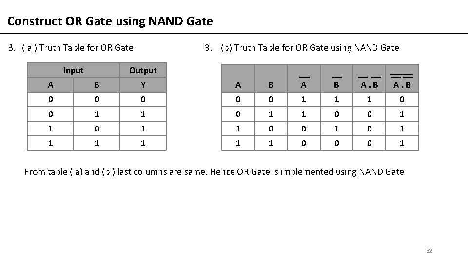
Construct OR Gate using NAND Gate 3. ( a ) Truth Table for OR Gate Input 3. (b) Truth Table for OR Gate using NAND Gate Output A B Y A B A. B 0 0 0 1 1 1 0 0 1 1 0 0 1 1 1 1 0 0 0 1 From table ( a) and (b ) last columns are same. Hence OR Gate is implemented using NAND Gate 32

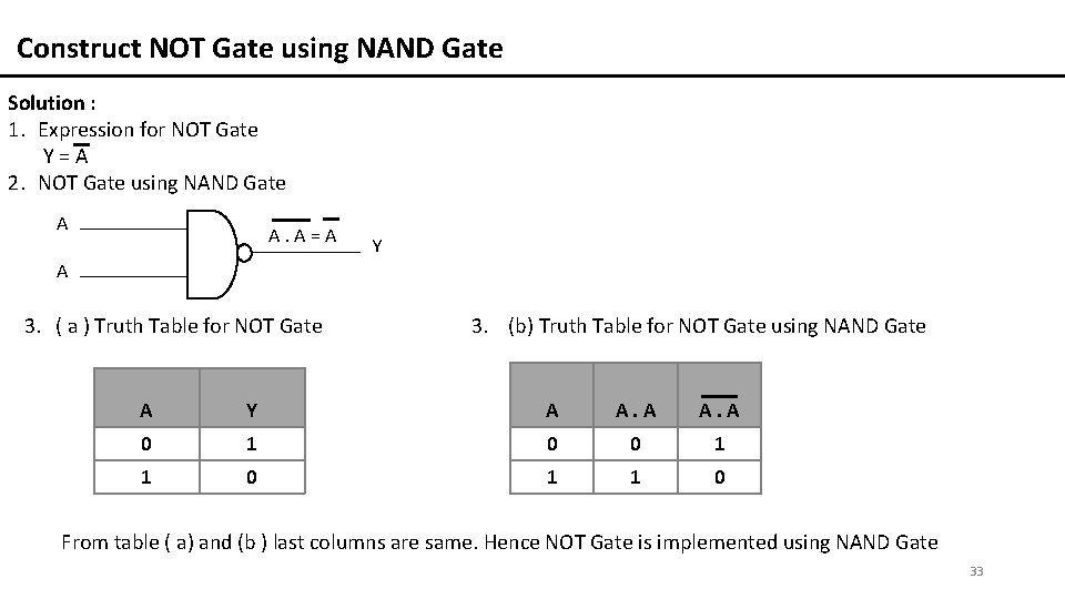
Construct NOT Gate using NAND Gate Solution : 1. Expression for NOT Gate Y=A 2. NOT Gate using NAND Gate A A. A=A Y A 3. ( a ) Truth Table for NOT Gate 3. (b) Truth Table for NOT Gate using NAND Gate A Y A A. A 0 1 0 0 1 1 0 From table ( a) and (b ) last columns are same. Hence NOT Gate is implemented using NAND Gate 33

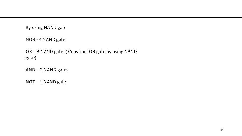
By using NAND gate NOR - 4 NAND gate OR - 3 NAND gate ( Construct OR gate by using NAND gate) AND - 2 NAND gates NOT - 1 NAND gate 34

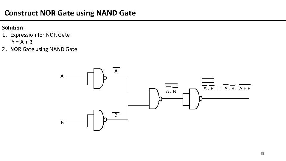
Construct NOR Gate using NAND Gate Solution : 1. Expression for NOR Gate Y=A+B 2. NOR Gate using NAND Gate A A A. B = A. B=A+B B B 35

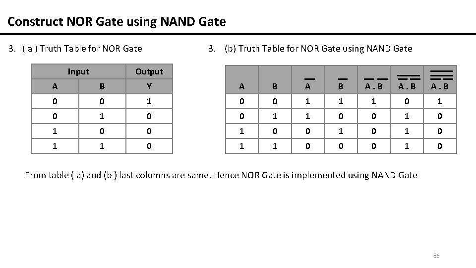
Construct NOR Gate using NAND Gate 3. ( a ) Truth Table for NOR Gate Input 3. (b) Truth Table for NOR Gate using NAND Gate Output A B Y A B A. B 0 0 1 1 1 0 1 0 0 1 0 1 1 0 0 0 1 0 From table ( a) and (b ) last columns are same. Hence NOR Gate is implemented using NAND Gate 36

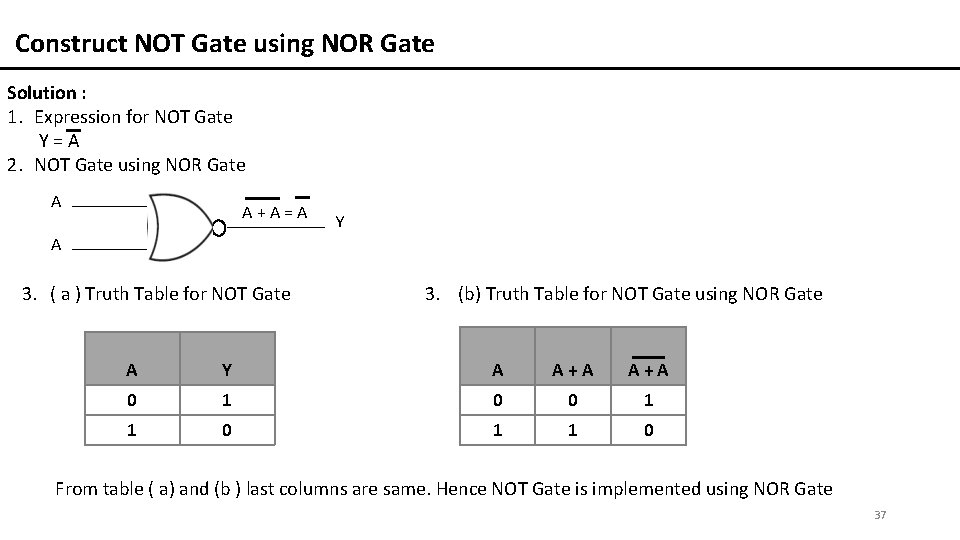
Construct NOT Gate using NOR Gate Solution : 1. Expression for NOT Gate Y=A 2. NOT Gate using NOR Gate A A+A=A Y A 3. ( a ) Truth Table for NOT Gate 3. (b) Truth Table for NOT Gate using NOR Gate A Y A A+A 0 1 0 0 1 1 0 From table ( a) and (b ) last columns are same. Hence NOT Gate is implemented using NOR Gate 37

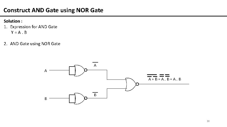
Construct AND Gate using NOR Gate Solution : 1. Expression for AND Gate Y=A. B 2. AND Gate using NOR Gate A A A+B=A. B B B 38

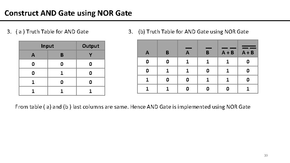
Construct AND Gate using NOR Gate 3. ( a ) Truth Table for AND Gate Input 3. (b) Truth Table for AND Gate using NOR Gate Output A B Y 0 0 1 1 1 A B A+B 0 0 1 1 1 0 0 1 1 0 0 0 1 From table ( a) and (b ) last columns are same. Hence AND Gate is implemented using NOR Gate 39

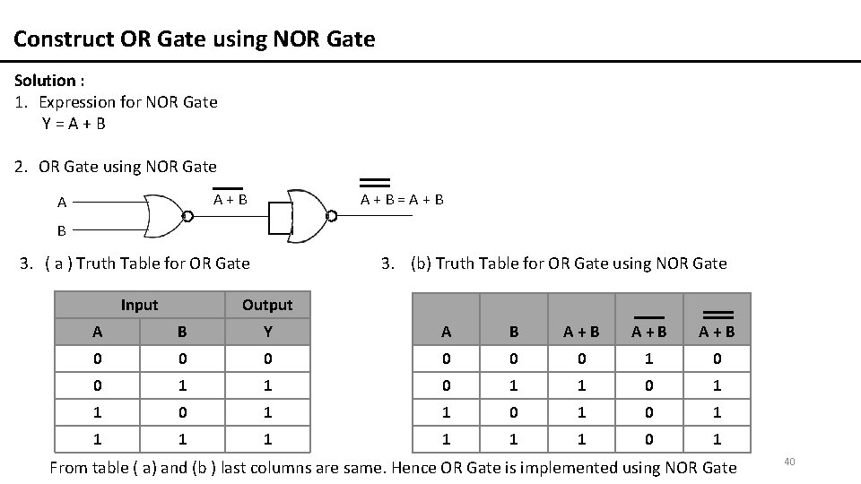
Construct OR Gate using NOR Gate Solution : 1. Expression for NOR Gate Y=A+B 2. OR Gate using NOR Gate A+B A A+B=A+B B 3. ( a ) Truth Table for OR Gate Input 3. (b) Truth Table for OR Gate using NOR Gate Output A B Y A B A+B A+B 0 0 0 1 1 0 1 1 1 1 0 1 From table ( a) and (b ) last columns are same. Hence OR Gate is implemented using NOR Gate 40

Construct NAND Gate using NOR Gate Solution : 1. Expression for NAND Gate Y=A. B 2. NAND Gate using NOR Gate A A A+B = A+B=A. B B B 41

Construct NAND Gate using NOR Gate 3. ( a ) Truth Table for NAND Gate Input 3. (b) Truth Table for NAND Gate using NOR Gate Output A B Y A B A+B A+B 0 0 1 1 1 0 1 0 1 1 0 0 1 1 1 0 0 0 1 0 From table ( a) and (b ) last columns are same. Hence NAND Gate is implemented using NOR Gate 42

43