Lecture 7 MultiLevel Gate Networks ANDOR network twolevel
![Convert POS to Other Forms • F = (A+B+C)(A+B’+C’)(A+C’+D) OR-AND = [{(A+B+C)(A+B’+C’)(A+C’+D)]’}’ = [(A+B+C)’ Convert POS to Other Forms • F = (A+B+C)(A+B’+C’)(A+C’+D) OR-AND = [{(A+B+C)(A+B’+C’)(A+C’+D)]’}’ = [(A+B+C)’](https://slidetodoc.com/presentation_image_h/9f6545a8a03fd4f4f3cbcb5a962aaa99/image-14.jpg)
- Slides: 30

Lecture 7 Multi-Level Gate Networks • AND-OR network: two-level – SOP expression. Using factoring to increase the number of levels. • OR-AND network: two-level – POS expression: Using multiplying out to increase the number of levels. – Why? • It may reduce the number of gates or gate inputs. • The number of gates which can be cascaded is limited by the gate delays. Chap 7 C-H 1

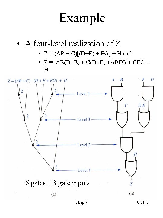
Example • A four-level realization of Z • Z = (AB + C)[(D+E) + FG] + H and • Z = AB(D+E) + C(D+E) +ABFG + CFG + H 6 gates, 13 gate inputs Chap 7 C-H 2

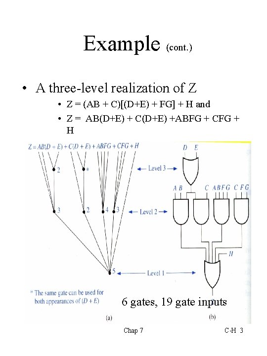
Example (cont. ) • A three-level realization of Z • Z = (AB + C)[(D+E) + FG] + H and • Z = AB(D+E) + C(D+E) +ABFG + CFG + H 6 gates, 19 gate inputs Chap 7 C-H 3

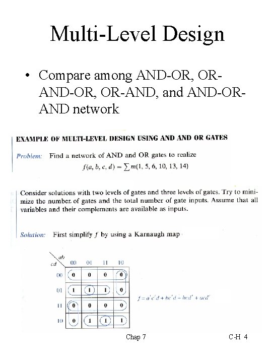
Multi-Level Design • Compare among AND-OR, OR-AND, and AND-ORAND network Chap 7 C-H 4

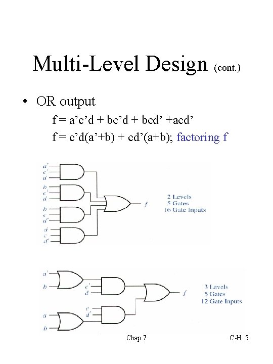
Multi-Level Design (cont. ) • OR output f = a’c’d + bcd’ +acd’ f = c’d(a’+b) + cd’(a+b); factoring f Chap 7 C-H 5

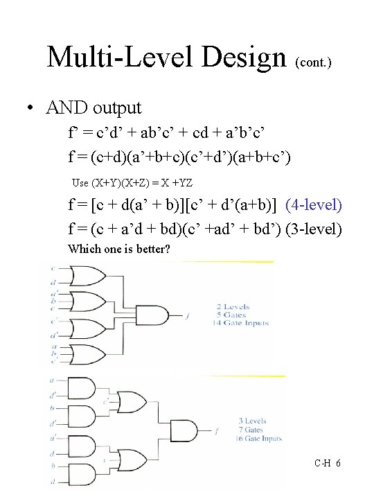
Multi-Level Design (cont. ) • AND output f’ = c’d’ + ab’c’ + cd + a’b’c’ f = (c+d)(a’+b+c)(c’+d’)(a+b+c’) Use (X+Y)(X+Z) = X +YZ f = [c + d(a’ + b)][c’ + d’(a+b)] (4 -level) f = (c + a’d + bd)(c’ +ad’ + bd’) (3 -level) Which one is better? Chap 7 C-H 6

Rule of Thumb • To find an OR output gate – Use SOP expression • f = a’c’d + bcd’ +acd’ – To find an OR-AND-OR gate network » Factor an SOP » f = c’d(a’+b) + cd’(a+b) • To find an AND output gate – Use POS expression • f’ =c’d’ + ab’c’ + cd +a’b’c (K-map) • Then use De. Morgan Law to find f • f = (c+d)(a’+b+c)(c’+d’)(a+b+c) – To find a three level network with AND output » Partially multiply out the POS expression » f = (c+a’d + bd)(c’+ad’ + bd’) Chap 7 C-H 7

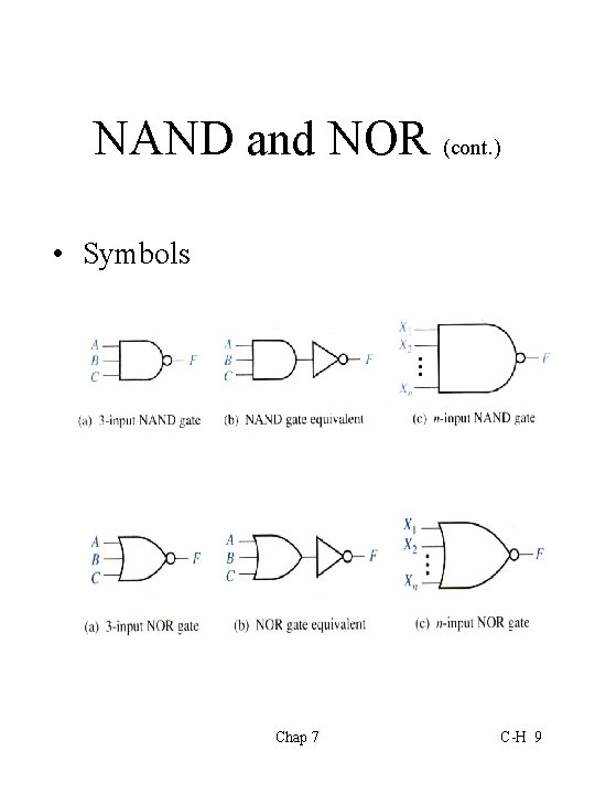
NAND and NOR Gate • NAND gate F = (ABC)’ = A’ + B’ + C’. F = 1 iff one or more of its inputs are 0. F = 0 if all inputs are 1. • NOR gate F = (A + B + C)’ = A’B’C’ F = 1 iff all inputs are 0. F = 0 if any input is 1. • NAND and NOR are duals. • If a given circuit realizes the NAND function for positive logic, it realizes the NOR function for negative logic. Chap 7 C-H 8

NAND and NOR (cont. ) • Symbols Chap 7 C-H 9

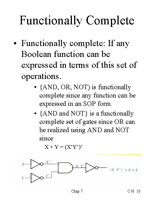
Functionally Complete • Functionally complete: If any Boolean function can be expressed in terms of this set of operations. • {AND, OR, NOT) is functionally complete since any function can be expressed in an SOP form. • {AND and NOT} is a functionally complete set of gates since OR can be realized using AND and NOT since X + Y = (X’Y’)’ Chap 7 C-H 10

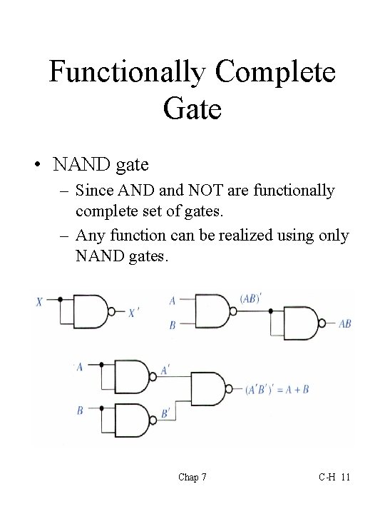
Functionally Complete Gate • NAND gate – Since AND and NOT are functionally complete set of gates. – Any function can be realized using only NAND gates. Chap 7 C-H 11

NAND and NOR why uses them? • In design using gate level IC, NAND and NOR are usually used because – They are faster than AND and OR gates. – NAND and NOR are functionally complete gates. • NAND is faster than NOR which has two PMOS in series and needs more area to have good and fall times. – More fan-ins variety to choose for NAND and NOR gate ICs. Chap 7 C-H 12

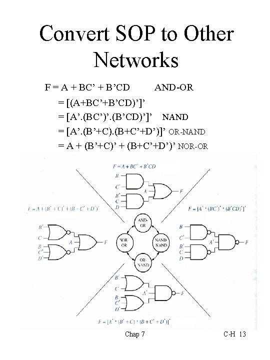
Convert SOP to Other Networks F = A + BC’ + B’CD AND-OR = [(A+BC’+B’CD)’]’ = [A’. (BC’)’. (B’CD)’]’ NAND = [A’. (B’+C). (B+C’+D’)]’ OR-NAND = A + (B’+C)’ + (B+C’+D’)’ NOR-OR Chap 7 C-H 13
![Convert POS to Other Forms F ABCABCACD ORAND ABCABCACD ABC Convert POS to Other Forms • F = (A+B+C)(A+B’+C’)(A+C’+D) OR-AND = [{(A+B+C)(A+B’+C’)(A+C’+D)]’}’ = [(A+B+C)’](https://slidetodoc.com/presentation_image_h/9f6545a8a03fd4f4f3cbcb5a962aaa99/image-14.jpg)
Convert POS to Other Forms • F = (A+B+C)(A+B’+C’)(A+C’+D) OR-AND = [{(A+B+C)(A+B’+C’)(A+C’+D)]’}’ = [(A+B+C)’ + (A+B’+C’)’ + (A+C’+D)’]’ NOR-NOR = (A’B’C’ + A’BC + A’CD’)’ AND-NOR = (A’B’C’)’. (A’BC)’. (A’CD’)’ NAND-AND Chap 7 C-H 14

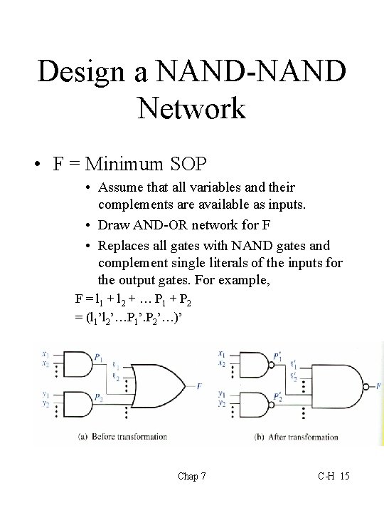
Design a NAND-NAND Network • F = Minimum SOP • Assume that all variables and their complements are available as inputs. • Draw AND-OR network for F • Replaces all gates with NAND gates and complement single literals of the inputs for the output gates. For example, F = l 1 + l 2 + … P 1 + P 2 = (l 1’l 2’…P 1’. P 2’…)’ Chap 7 C-H 15

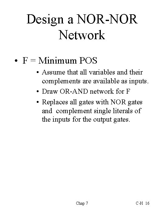
Design a NOR-NOR Network • F = Minimum POS • Assume that all variables and their complements are available as inputs. • Draw OR-AND network for F • Replaces all gates with NOR gates and complement single literals of the inputs for the output gates. Chap 7 C-H 16

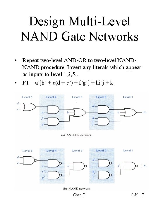
Design Multi-Level NAND Gate Networks • Repeat two-level AND-OR to two-level NAND procedure. Invert any literals which appear as inputs to level 1, 3, 5. . • F 1 = a’[b’ + c(d + e’) + f’g’] + hi’j + k Chap 7 C-H 17

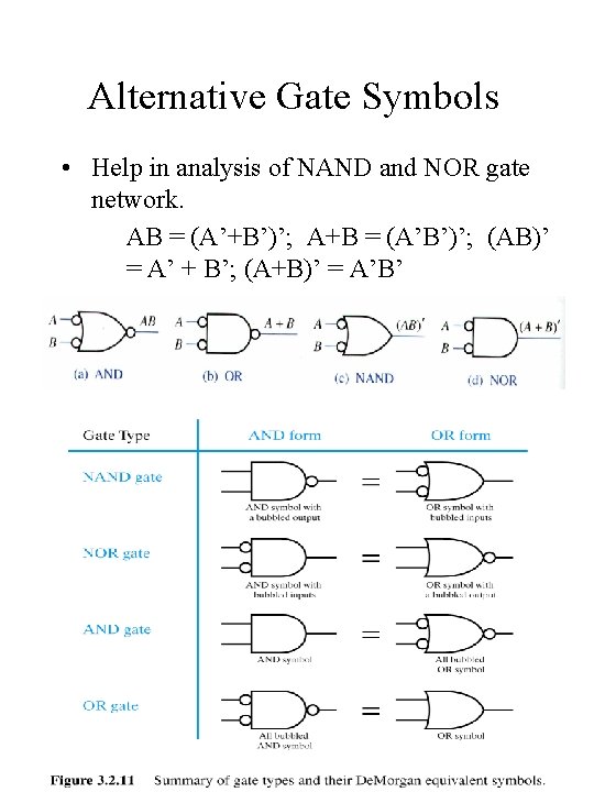
Alternative Gate Symbols • Help in analysis of NAND and NOR gate network. AB = (A’+B’)’; A+B = (A’B’)’; (AB)’ = A’ + B’; (A+B)’ = A’B’ Chap 7 C-H 18

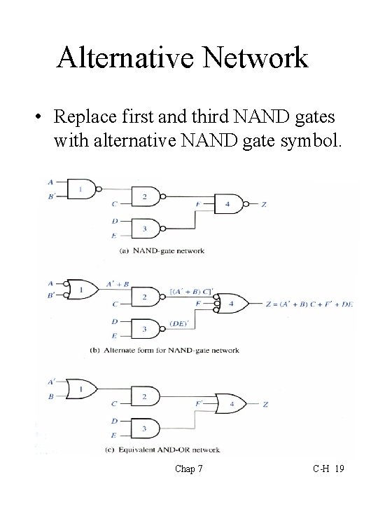
Alternative Network • Replace first and third NAND gates with alternative NAND gate symbol. Chap 7 C-H 19

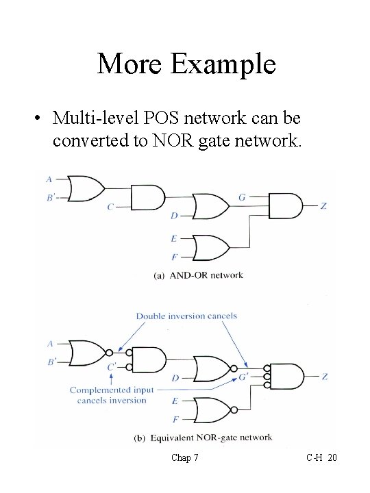
More Example • Multi-level POS network can be converted to NOR gate network. Chap 7 C-H 20

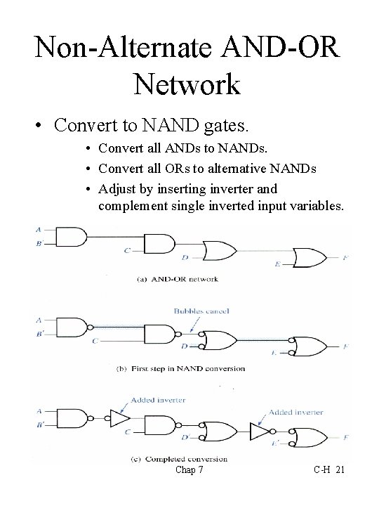
Non-Alternate AND-OR Network • Convert to NAND gates. • Convert all ANDs to NANDs. • Convert all ORs to alternative NANDs • Adjust by inserting inverter and complement single inverted input variables. Chap 7 C-H 21

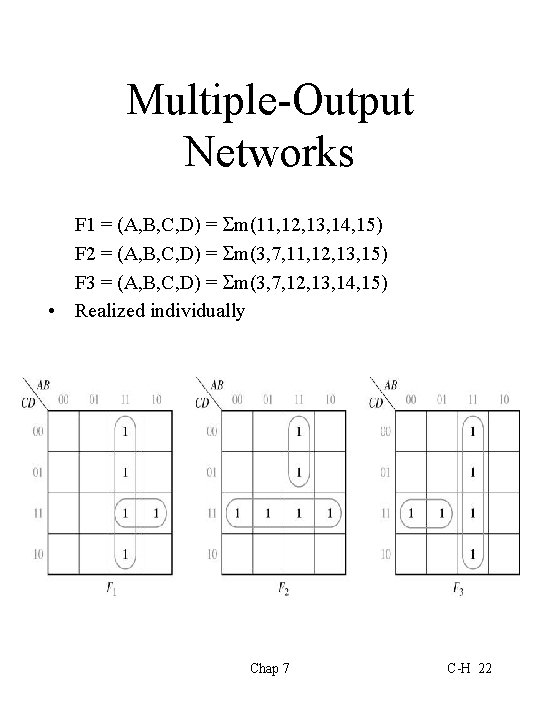
Multiple-Output Networks F 1 = (A, B, C, D) = m(11, 12, 13, 14, 15) F 2 = (A, B, C, D) = m(3, 7, 11, 12, 13, 15) F 3 = (A, B, C, D) = m(3, 7, 12, 13, 14, 15) • Realized individually Chap 7 C-H 22

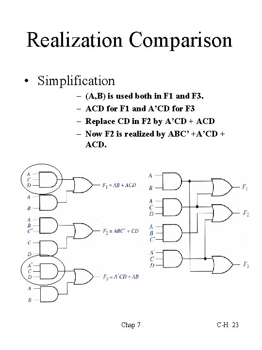
Realization Comparison • Simplification – – (A, B) is used both in F 1 and F 3. ACD for F 1 and A’CD for F 3 Replace CD in F 2 by A’CD + ACD Now F 2 is realized by ABC’ +A’CD + ACD. Chap 7 C-H 23

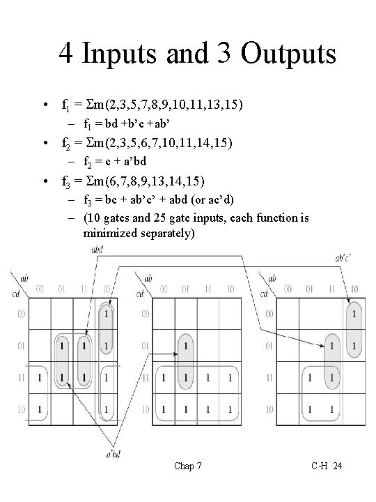
4 Inputs and 3 Outputs • f 1 = m(2, 3, 5, 7, 8, 9, 10, 11, 13, 15) – f 1 = bd +b’c +ab’ • f 2 = m(2, 3, 5, 6, 7, 10, 11, 14, 15) – f 2 = c + a’bd • f 3 = m(6, 7, 8, 9, 13, 14, 15) – f 3 = bc + ab’c’ + abd (or ac’d) – (10 gates and 25 gate inputs, each function is minimized separately) Chap 7 C-H 24

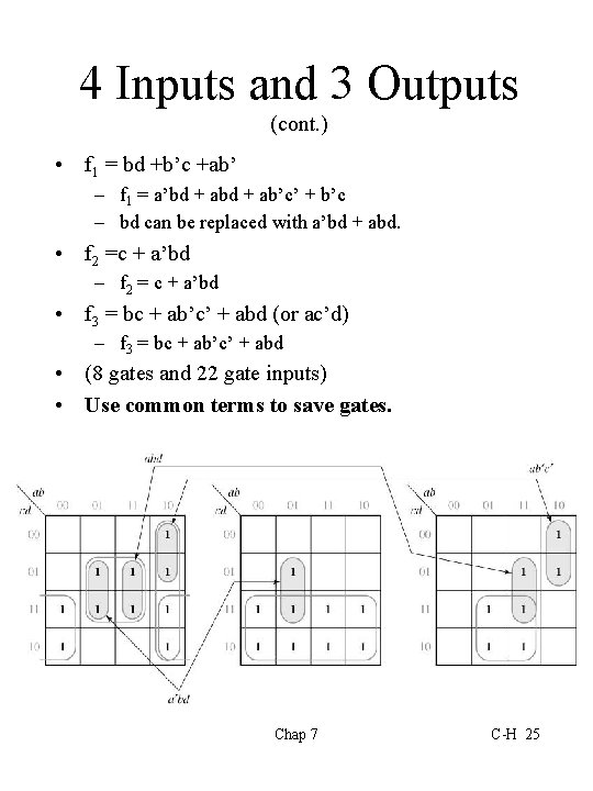
4 Inputs and 3 Outputs (cont. ) • f 1 = bd +b’c +ab’ – f 1 = a’bd + ab’c’ + b’c – bd can be replaced with a’bd + abd. • f 2 =c + a’bd – f 2 = c + a’bd • f 3 = bc + ab’c’ + abd (or ac’d) – f 3 = bc + ab’c’ + abd • (8 gates and 22 gate inputs) • Use common terms to save gates. Chap 7 C-H 25

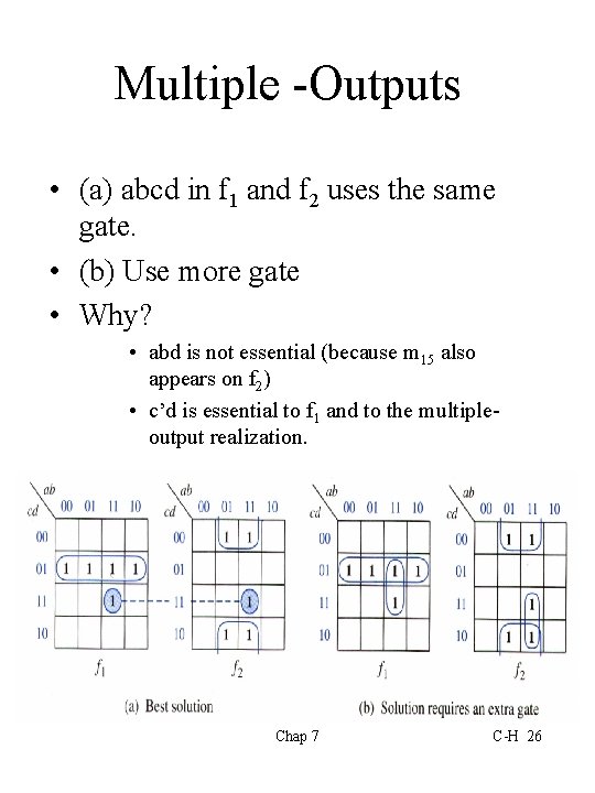
Multiple -Outputs • (a) abcd in f 1 and f 2 uses the same gate. • (b) Use more gate • Why? • abd is not essential (because m 15 also appears on f 2) • c’d is essential to f 1 and to the multipleoutput realization. Chap 7 C-H 26

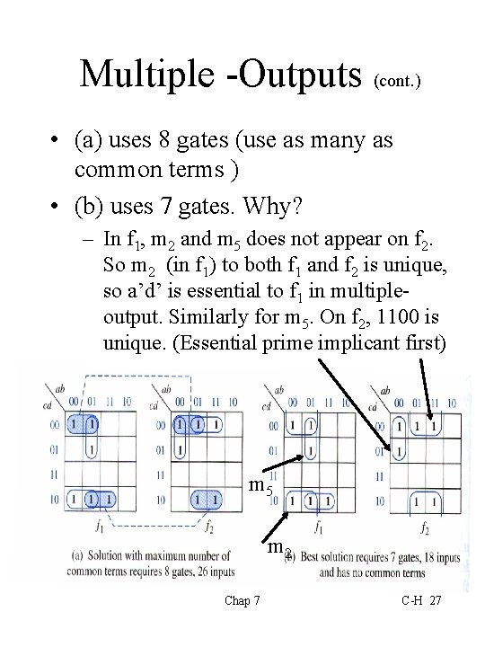
Multiple -Outputs (cont. ) • (a) uses 8 gates (use as many as common terms ) • (b) uses 7 gates. Why? – In f 1, m 2 and m 5 does not appear on f 2. So m 2 (in f 1) to both f 1 and f 2 is unique, so a’d’ is essential to f 1 in multipleoutput. Similarly for m 5. On f 2, 1100 is unique. (Essential prime implicant first) m 5 m 2 Chap 7 C-H 27

Multiple-Output Optimization • Find the essential prime implicants for the multiple output. • Checking for common terms to see if using them will help. Chap 7 C-H 28

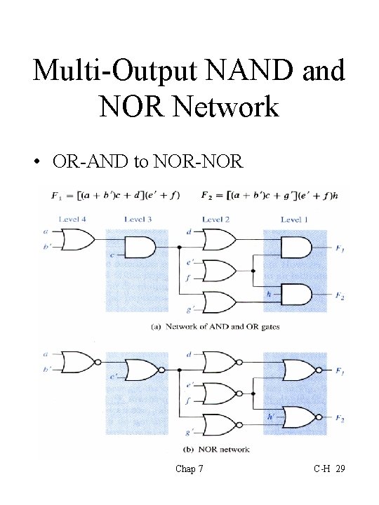
Multi-Output NAND and NOR Network • OR-AND to NOR-NOR Chap 7 C-H 29

Terminology • Terms: – Fan-out: the maximum number of inputs to which an IC output can be connected without electrically loading down the output. – Fan in: the number of inputs to a gate. – PCB: printed circuit board. – HDL: hardware description language. – Synthesis: when a logic circuit is obtained from a functional description (equation or truth table). This process is called synthesis. Chap 7 C-H 30