CHAPTER 6 Virtex Memory Agenda RAM Applications LUT

- Slides: 45

CHAPTER 6 Virtex Memory

Agenda • RAM Applications • LUT RAM – SRL 16 – Other uses of LUT RAM (FIFO focus) • Block RAM • Inside Block RAM Cells

RAM Applications • • • Operand stacks Register files Instruction caches DMA buffers Instruction memories State tables Logic functions Message buffers Virtual channels • Video line buffers • Digital delay lines • RAMDAC color mapping tables • Test vector buffers • PCI configuration space • Sequential machines • More. . .

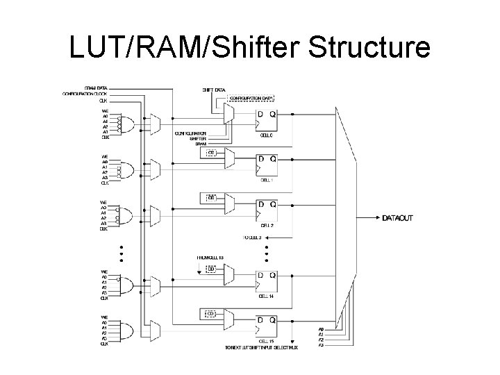
LUT/RAM/Shifter Structure

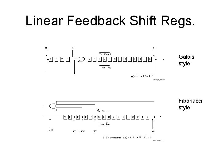
Linear Feedback Shift Regs. Galois style Fibonacci style

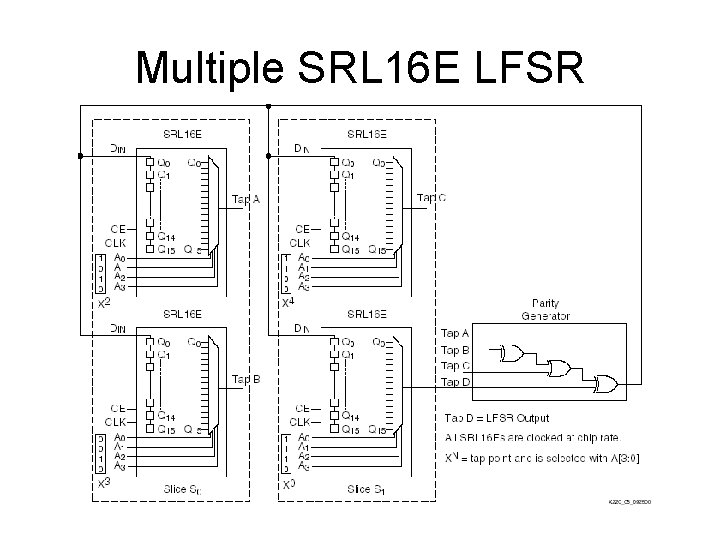
Multiple SRL 16 E LFSR

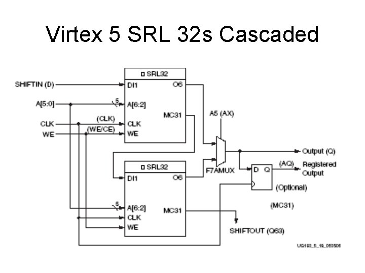
Virtex 5 SRL 32 s Cascaded

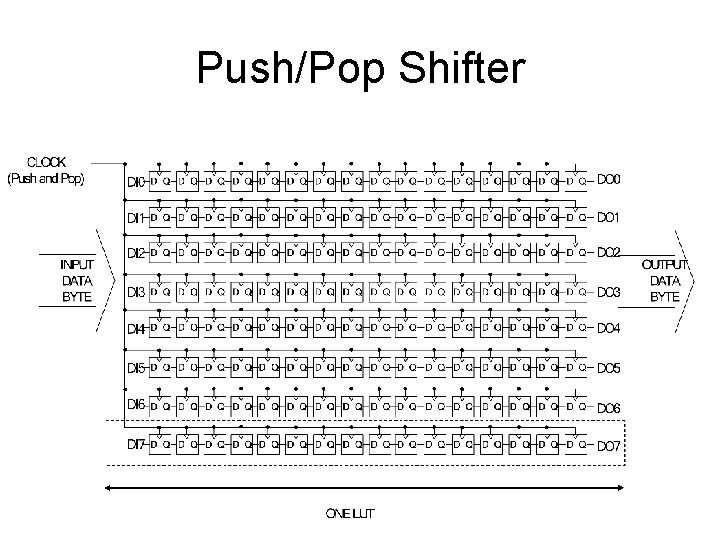
Push/Pop Shifter

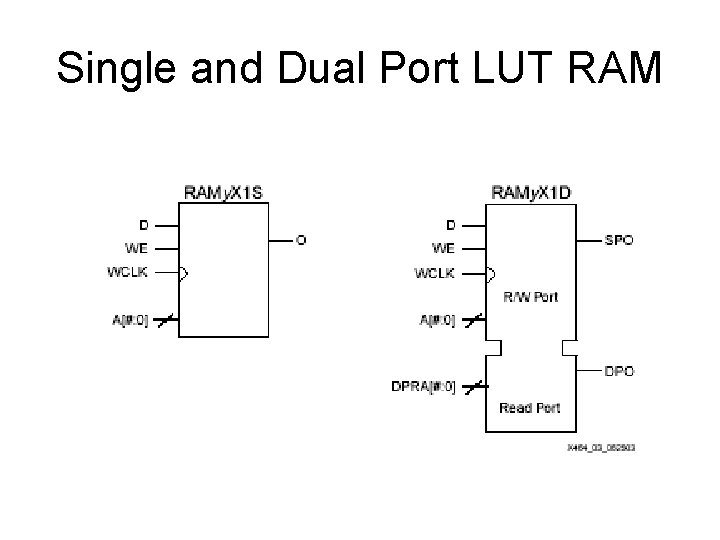
Single and Dual Port LUT RAM

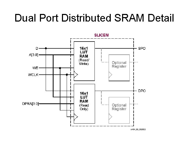
Dual Port Distributed SRAM Detail

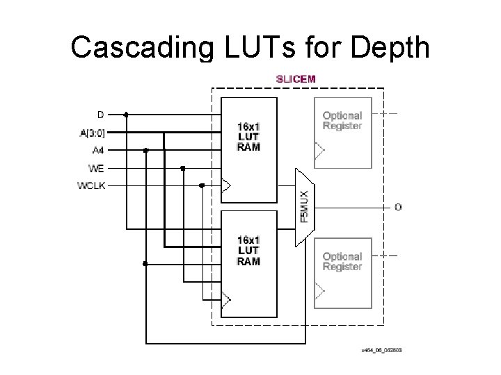
Cascading LUTs for Depth

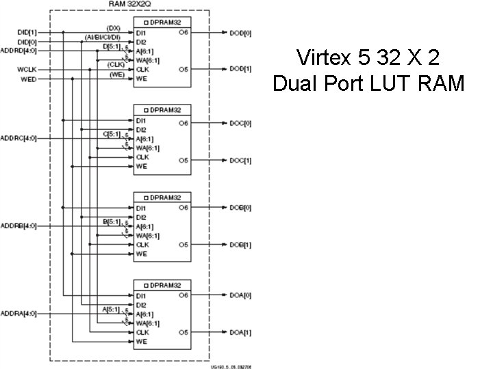
Virtex 5 32 X 2 Dual Port LUT RAM

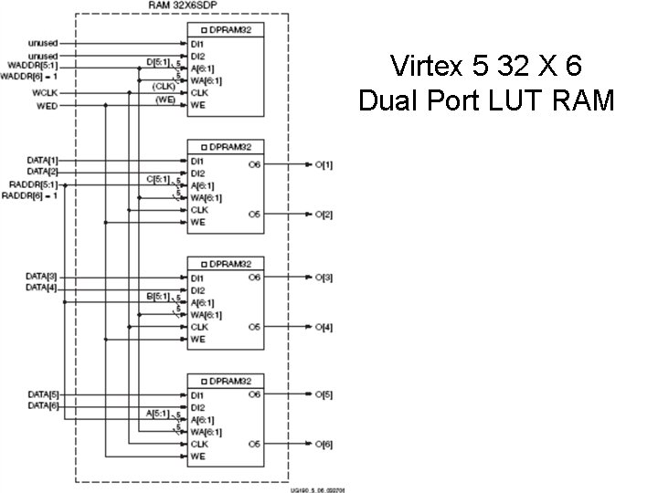
Virtex 5 32 X 6 Dual Port LUT RAM

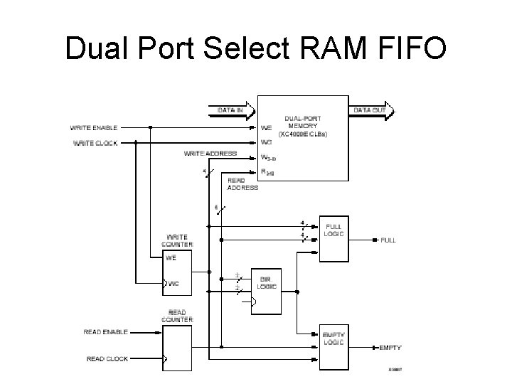
Dual Port Select RAM FIFO

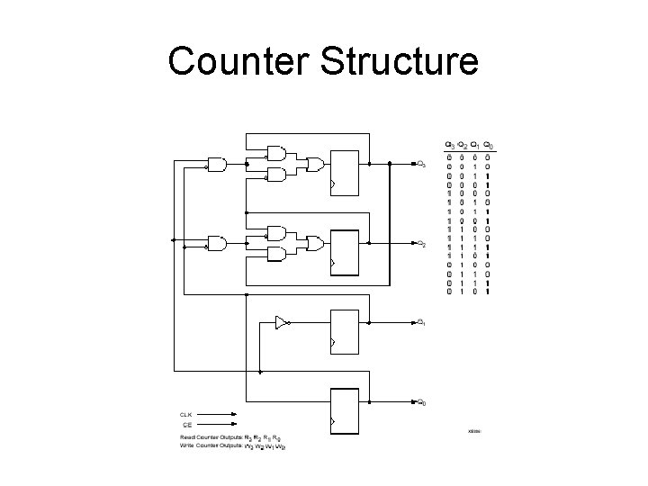
Counter Structure

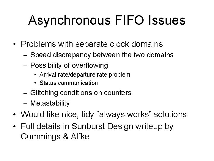
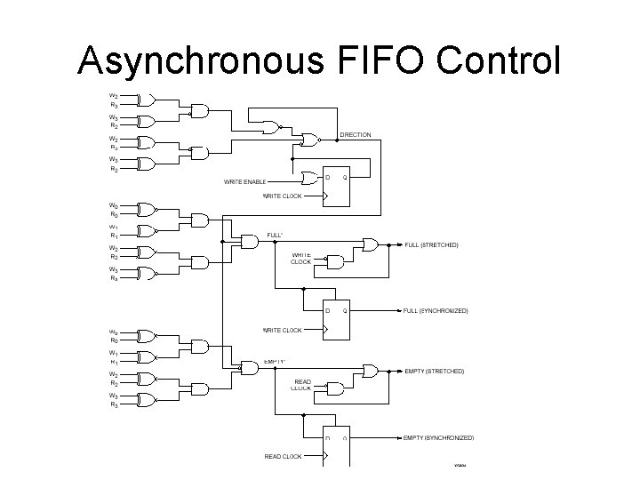
Asynchronous FIFO Issues • Problems with separate clock domains – Speed discrepancy between the two domains – Possibility of overflowing • Arrival rate/departure rate problem • Status communication – Glitching conditions on counters – Metastability • Would like nice, tidy “always works” solutions • Full details in Sunburst Design writeup by Cummings & Alfke

Asynchronous FIFO Control

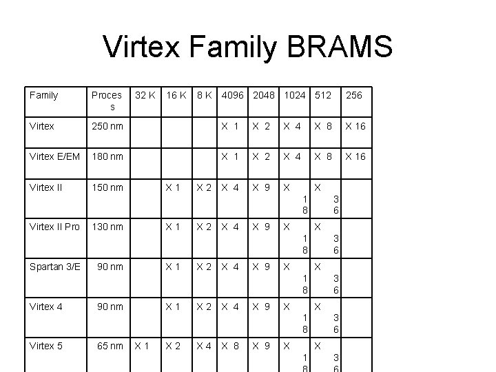
Virtex Family BRAMS Family Proces s Virtex 32 K 16 K 4096 2048 1024 512 256 250 nm X 1 X 2 X 4 X 8 X 16 Virtex E/EM 180 nm X 1 X 2 X 4 X 8 X 16 Virtex II 150 nm X 4 X 9 X X X 1 8 K X 2 1 8 Virtex II Pro 130 nm X 1 X 2 X 4 X 9 X 3 6 X 1 8 Spartan 3/E 90 nm X 1 X 2 X 4 X 9 X 3 6 X 1 8 Virtex 4 90 nm X 1 X 2 X 4 X 9 X 3 6 X 1 8 Virtex 5 65 nm X 1 X 2 X 4 X 8 X 9 X 3 6 X 1 3

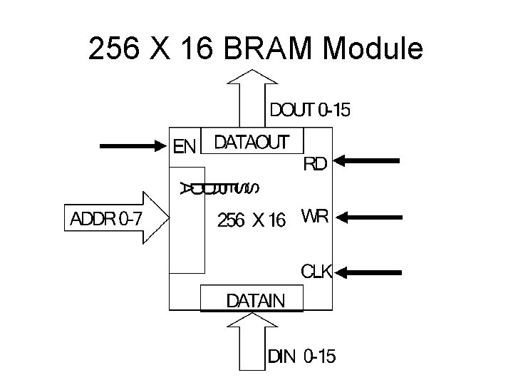
256 X 16 BRAM Module

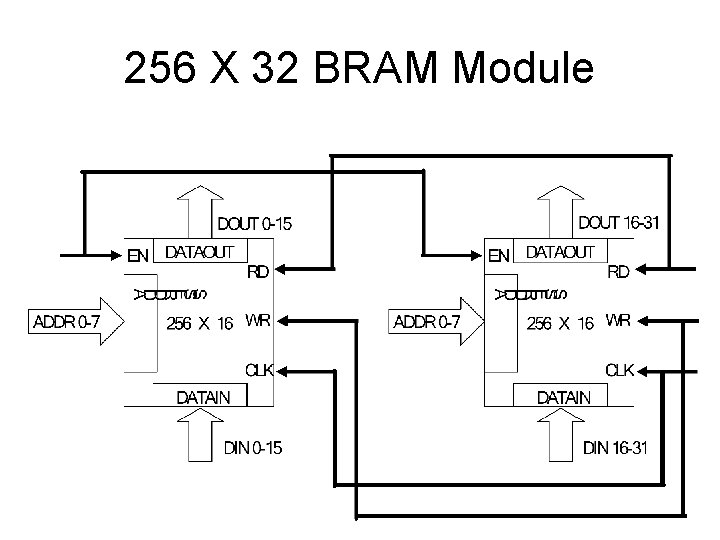
256 X 32 BRAM Module

512 X 16 BRAM Module Comment: slide needs Inverter on one of the EN’s

BRAM Specialized Interconnect

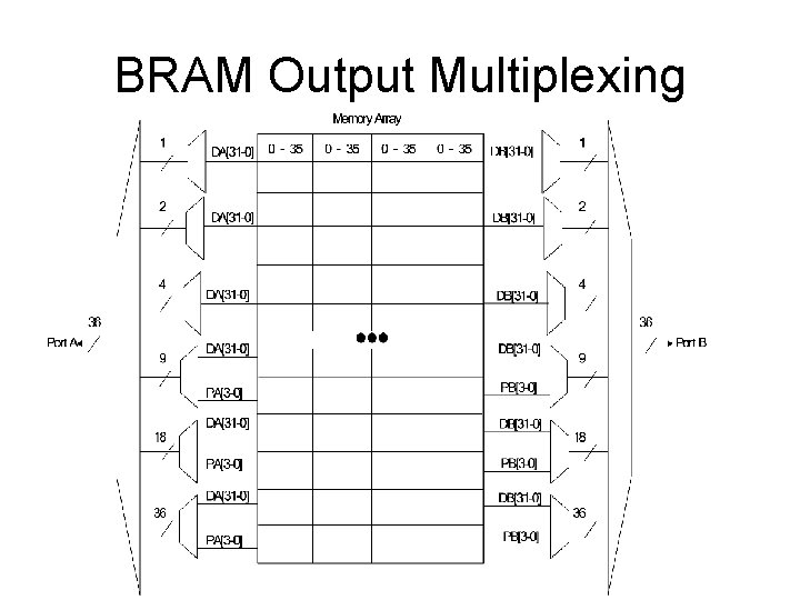
BRAM Output Multiplexing

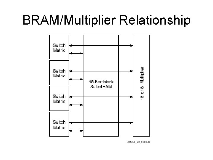
BRAM/Multiplier Relationship

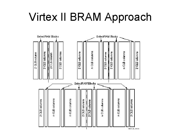
Virtex II BRAM Approach

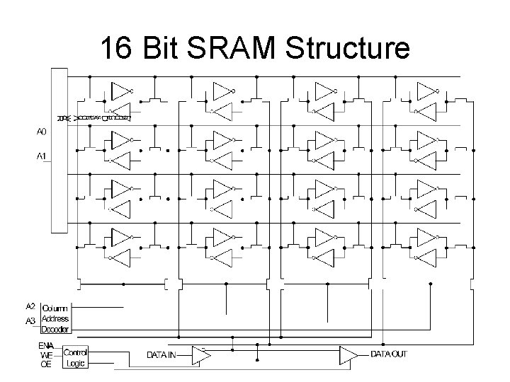
16 Bit SRAM Structure

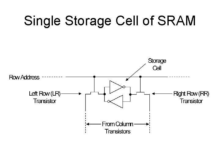
Single Storage Cell of SRAM

Single Bit SRAM Read/Write Circuits

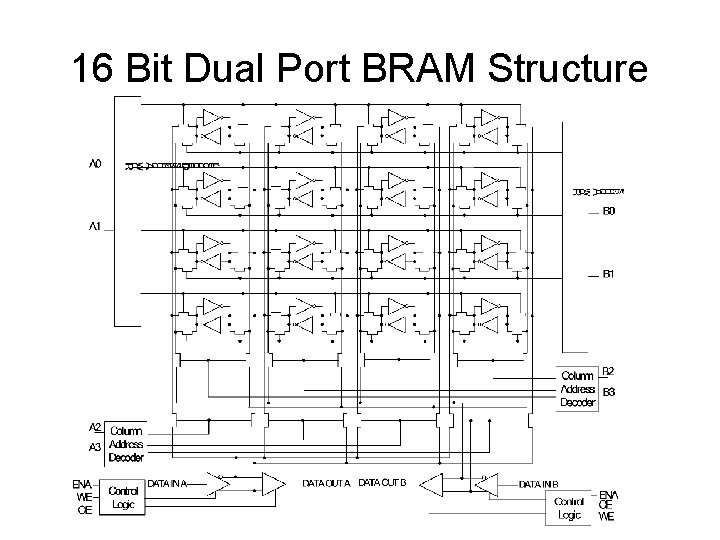
16 Bit Dual Port BRAM Structure

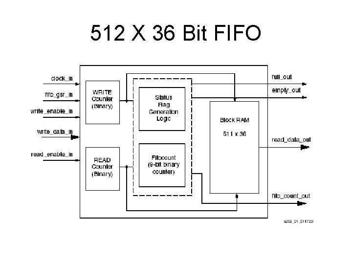
512 X 36 Bit FIFO

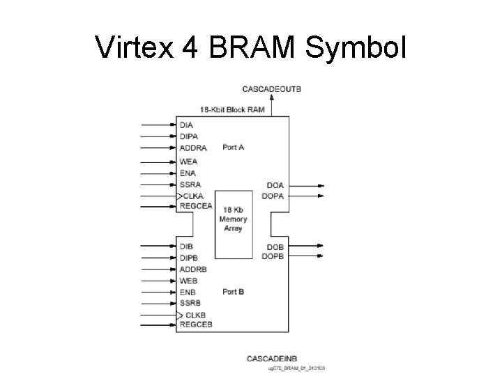
Virtex 4 BRAM Symbol

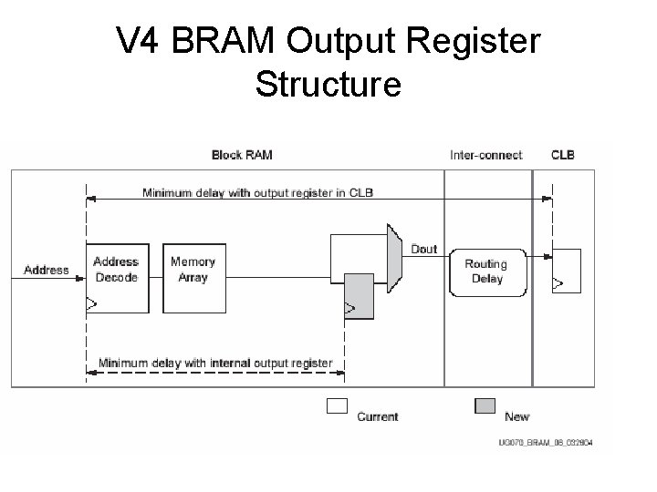
V 4 BRAM Output Register Structure

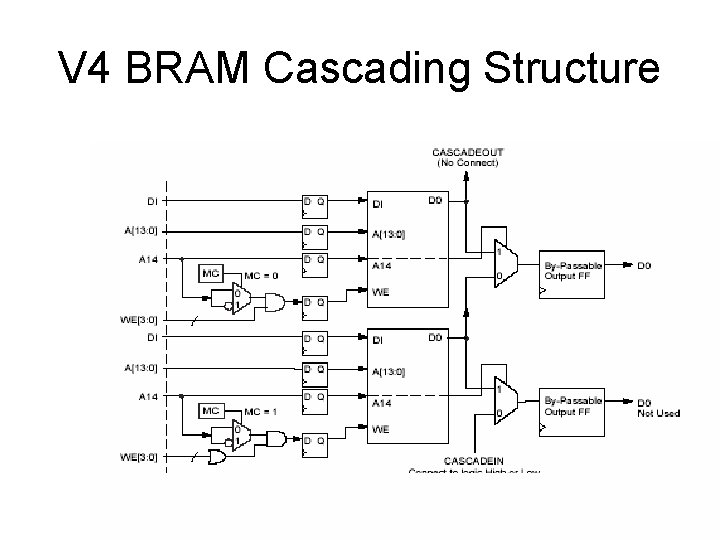
V 4 BRAM Cascading Structure

Virtex 4 FIFO Support Structure (this stuff is inside the V 4 BRAM module, built in)

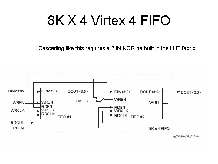
8 K X 4 Virtex 4 FIFO Cascading like this requires a 2 IN NOR be built in the LUT fabric

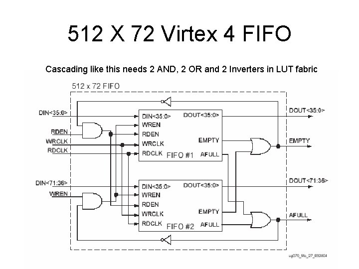
512 X 72 Virtex 4 FIFO Cascading like this needs 2 AND, 2 OR and 2 Inverters in LUT fabric

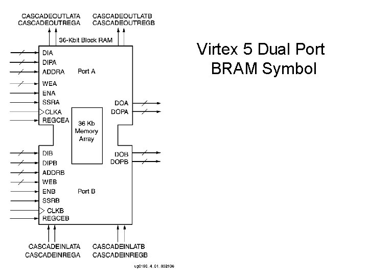
Virtex 5 Dual Port BRAM Symbol

Virtex 5 BRAM Organized X 64

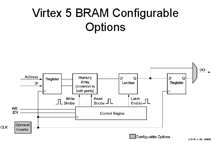
Virtex 5 BRAM Configurable Options

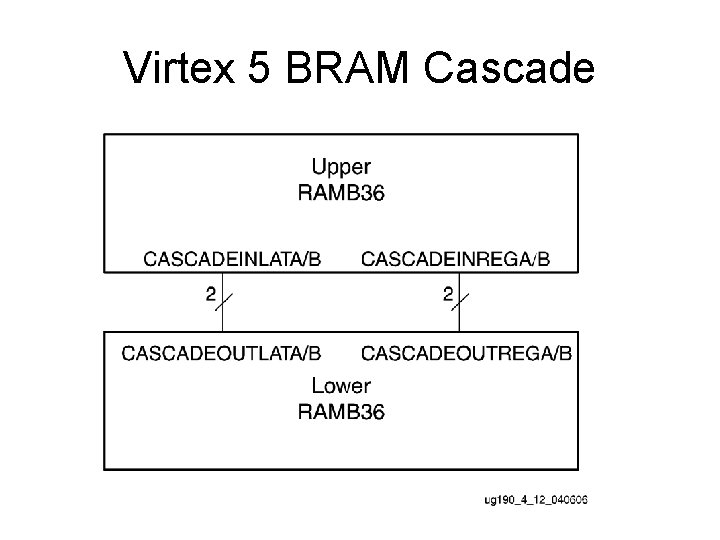
Virtex 5 BRAM Cascade

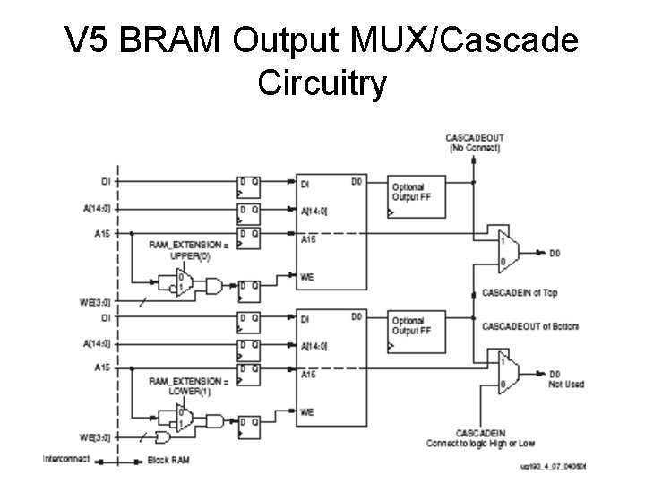
V 5 BRAM Output MUX/Cascade Circuitry

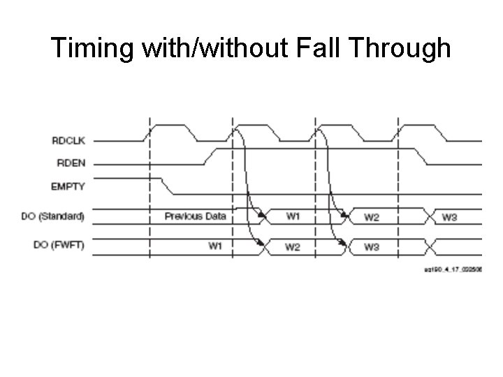
Timing with/without Fall Through

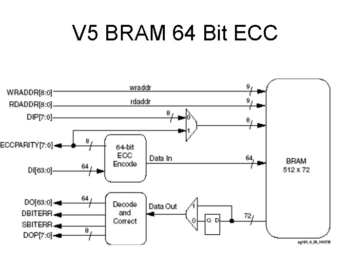
V 5 BRAM 64 Bit ECC

Virtex RAM Closing Comments • RAM may be the primary on board feature beyond fabric of general use • Makes having other on board resources more effective – – FIFOs –fast cross clock domain interfacing Microprocessors – code/data storage DSPs – on chip operand storage And so on. . . • See XAPP 463 (appendix) for Verilog/VHDL code listing for using BRAM structure.
