Memory ROM RAM CACHE Processor Cache Main Memory


 • External (secondary)")


")

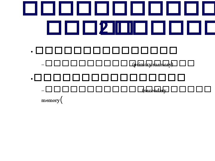
 ������ non-valatile • RAM (Random Access Memory) ������� valatitle")

 EPROM (Eraseable PROM) EEPROM (Electrical")
 • Dynamic RAM (DRAM)")

 DRAM SDRAM")


 • RDRAM (Rambus DRAM)")


- Slides: 42
����� (Memory( • ROM • RAM • CACHE Processor Cache Main Memory Virtual Memory
Characteristics • • Location Capacity Unit of transfer Access method Performance Physical type Physical characteristics Organisation
Location • CPU • Internal (main) • External (secondary)
Capacity • Word size – The natural unit of organization • Number of words – or Bytes
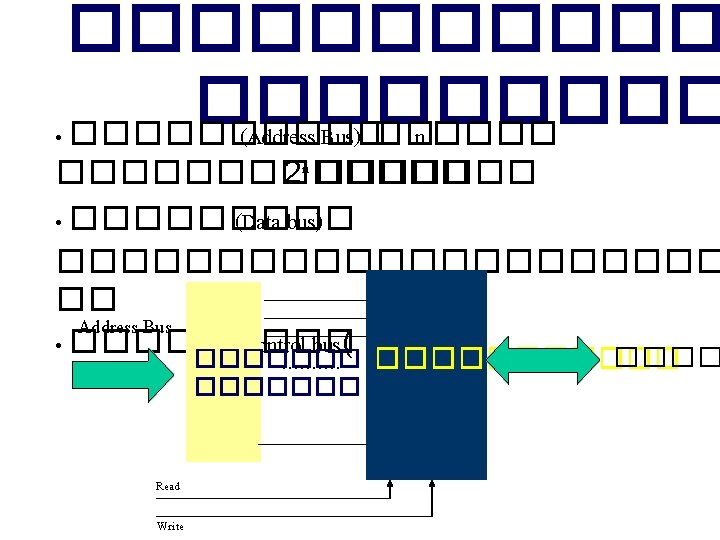
Unit of Transfer • Internal – Usually governed by data bus width • External – Usually a block which is much larger than a word • Addressable unit – Smallest location which can be uniquely addressed • Byte (sometimes) • Word internally • Cluster on disks
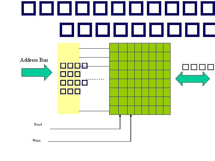
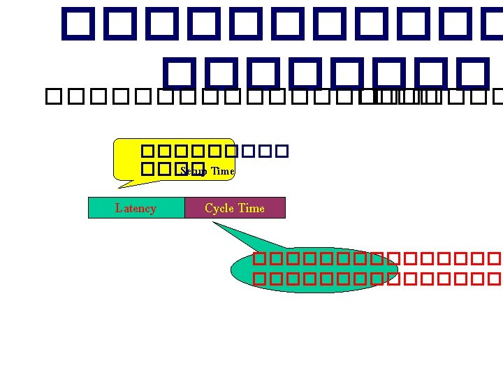
Performance • Access time – Time between presenting the address and getting the valid data • Memory Cycle time – Time may be required for the memory to “recover” before next access – Cycle time is access + recovery • Transfer Rate – Rate at which data can be moved
Memory Hierarchy • Registers – In CPU • Internal or Main memory – May include one or more levels of cache – “RAM” • External memory – Backing store
Hierarchy List • • Registers L 1 Cache L 2 Cache Main memory Disk cache Disk Optical Tape
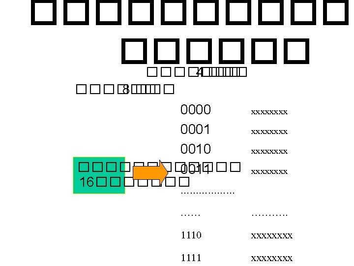
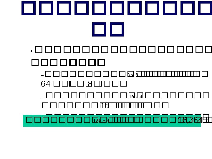
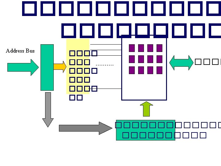
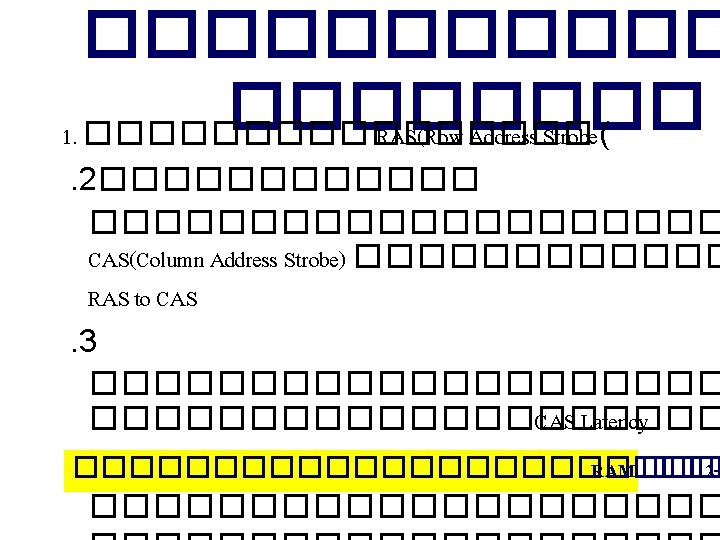
Organisation in detail • A 16 Mbit chip can be organised as 1 M of 16 bit words • A bit per chip system has 16 lots of 1 Mbit chip with bit 1 of each word in chip 1 and so on • A 16 Mbit chip can be organised as a 2048 x 4 bit array – Reduces number of address pins • Multiplex row address and column address • 11 pins to address (211=2048) • Adding one more pin doubles range of values so x 4 capacity
Typical 16 Mb DRAM (4 M x 4)
Packaging
������ • ROM (Read-Only Memory) ������ non-valatile • RAM (Random Access Memory) ������� valatitle – ���������� random access �����
FSB = 133 MHz Effective = 533 MHz Effective = 266 MHz CPU x 23 RAM 3. 06 GHz
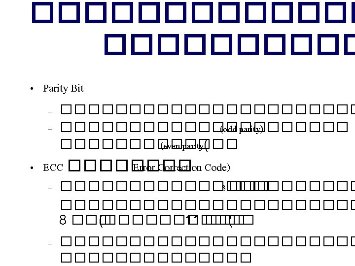
����� ROM • • • ROM PROM (Programmable ROM) EPROM (Eraseable PROM) EEPROM (Electrical EPROM) Flash ROM ���� Flash Memory
����� RAM • Static RAM (SRAM) • Dynamic RAM (DRAM)
������ 8 bits ROM 256 x 4 4 bit 8 bits ROM 256 x 4
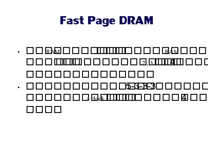
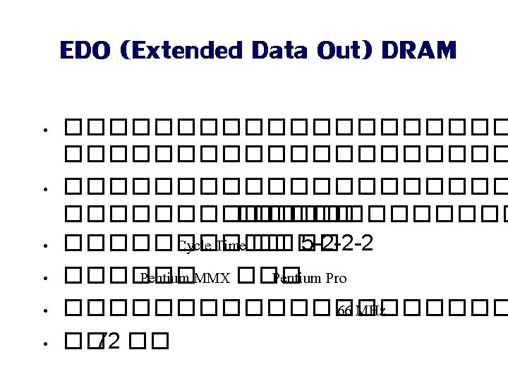
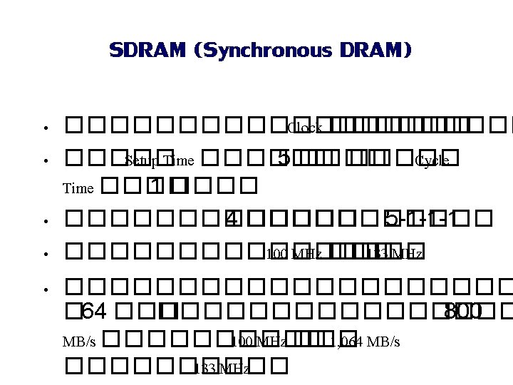
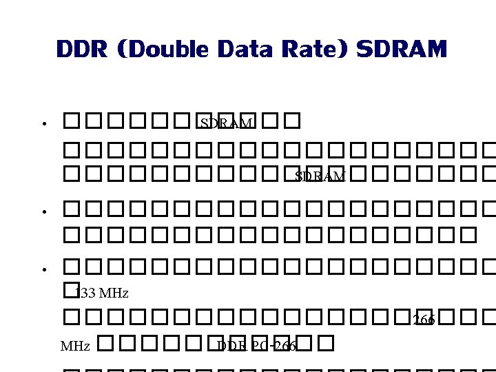
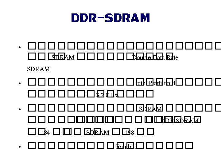
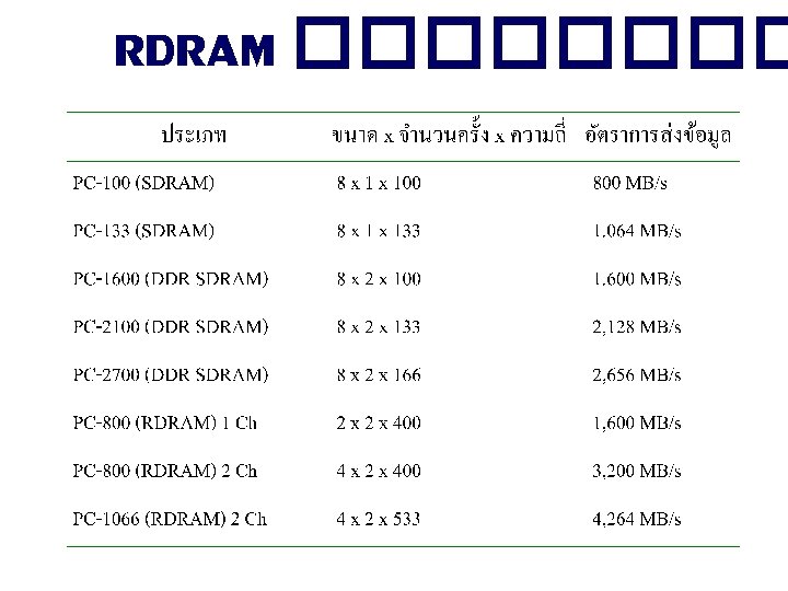
������ DRAM • • • Fast Page DRAM EDO (Extended Data Out) DRAM SDRAM (Synchronous DRAM) DDR (Double Data Rate) SDRAM RDRAM (Rambus DRAM)
DDR-SDRAM 15 10 5 20 clock DRAM 5 -5 -5 -5 Setup Cycle Setup 14 clock FPM RAM 5 -3 -3 -3 Setup Cycle EDO RAM 5 -2 -2 -2 Setup Cycle SDRAM 5 -1 -1 -1 Setup Cycle c Cycle Cycle 8 clock 11 clock
DDR-SDRAM Clock SDR Data Write DDR Data W W Write W W Read R R
RDRAM (Rambus DRAM) • RDRAM (Rambus DRAM)
Cache Memory Cache Controller CPU “Cache Hit” “Cache Miss” �������� (DRAM(
Cache ����� 16 k ��� 32 k ������� L 1 Instruction Cache L 2 Data Cache 128 k ��� 2 M ��������