Chapter 5 Enhanced Direct Memory Access EDMA Learning
![EDMA Parameters Index: Chapter 5, Slide 19 Upper 16 bits [31: 16]: Frame index. EDMA Parameters Index: Chapter 5, Slide 19 Upper 16 bits [31: 16]: Frame index.](https://slidetodoc.com/presentation_image_h/f88ce128b28b152ae6af0e7507e0cc61/image-19.jpg)
- Slides: 70

Chapter 5 Enhanced Direct Memory Access (EDMA)

Learning Objectives The need for a DMA (EDMA). Terms and definitions (with examples). EDMA functionality, including: Programming the EDMA, including: Chapter 5, Slide 2 Transfer modes and synchronisation. EDMA interrupt. Quick DMA (QDMA). Using the Chip Support Library (CSL). Example “inout” program using Ping. Pong EDMA.

The Need for a DMA There are two methods for transferring data from one part of the memory to another, these are using: (1) (2) Chapter 5, Slide 3 CPU. DMA. If a DMA is used then the CPU only needs to configure the DMA. Whilst the transfer is taking place the CPU is then free to perform other operations.

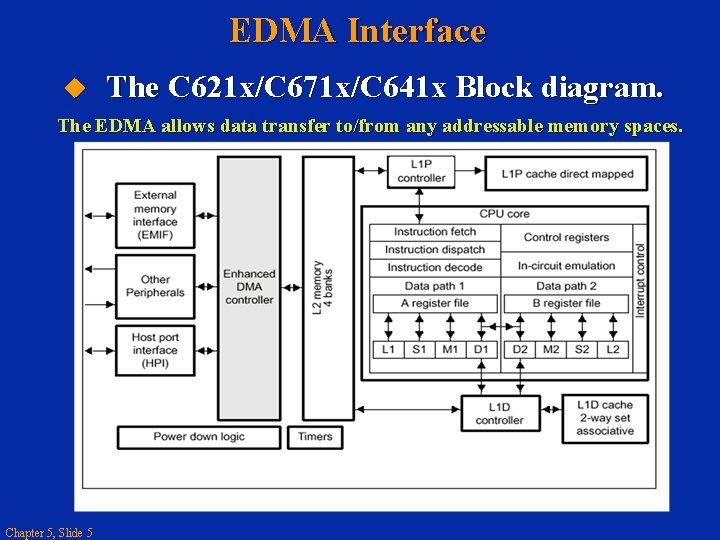
Introduction to the EDMA The ‘C 6211/C 6711 on-chip EDMA controller allows data transfers between the level two (L 2) cache memory controller and the device peripherals. These transfers include: Chapter 5, Slide 4 Cache servicing. Non-cacheable memory accesses. User programmed data transfers. Host accesses.

EDMA Interface The C 621 x/C 671 x/C 641 x Block diagram. The EDMA allows data transfer to/from any addressable memory spaces. Chapter 5, Slide 5

EDMA Functionality Chapter 5, Slide 6 The data transfer is performed with zero overhead. It is transparent to the CPU which means that the EDMA and CPU operations can be independent. However, if the EDMA and CPU both try to access the same memory location arbitration will be performed by the program memory controller.

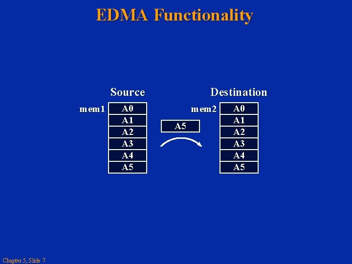
EDMA Functionality Source mem 1 Chapter 5, Slide 7 A 0 A 1 A 2 A 3 A 4 A 5 Destination mem 2 A 5 A 0 A 1 A 2 A 3 A 4 A 5

EDMA Features The ‘C 6211/C 6711 on-chip EDMA controller has the following features: Chapter 5, Slide 8 16 channels. 1 auxiliary channel dedicated for the HPI (not accessible to the user). 1 Quick DMA (QDMA).

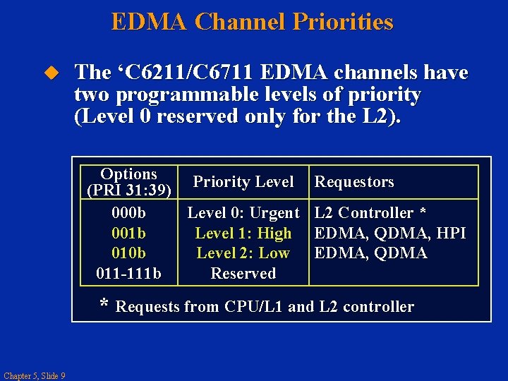
EDMA Channel Priorities The ‘C 6211/C 6711 EDMA channels have two programmable levels of priority (Level 0 reserved only for the L 2). Options (PRI 31: 39) Priority Level 000 b Level 0: Urgent 001 b Level 1: High 010 b Level 2: Low 011 -111 b Reserved Requestors L 2 Controller * EDMA, QDMA, HPI EDMA, QDMA * Requests from CPU/L 1 and L 2 controller Chapter 5, Slide 9

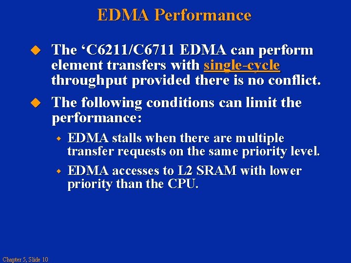
EDMA Performance The ‘C 6211/C 6711 EDMA can perform element transfers with single-cycle throughput provided there is no conflict. The following conditions can limit the performance: Chapter 5, Slide 10 EDMA stalls when there are multiple transfer requests on the same priority level. EDMA accesses to L 2 SRAM with lower priority than the CPU.

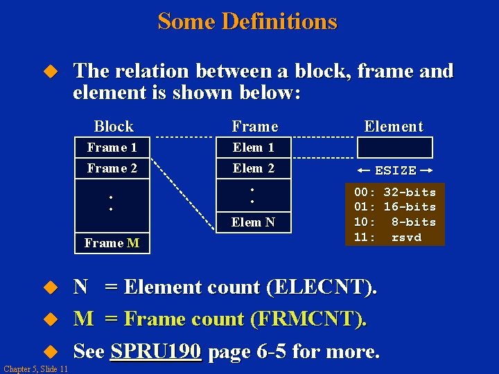
Some Definitions The relation between a block, frame and element is shown below: Block Frame Element Frame 1 Frame 2 Elem 1 Elem 2 ESIZE . . Frame M Chapter 5, Slide 11 . . Elem N 00: 32 -bits 01: 16 -bits 10: 8 -bits 11: rsvd N = Element count (ELECNT). M = Frame count (FRMCNT). See SPRU 190 page 6 -5 for more.

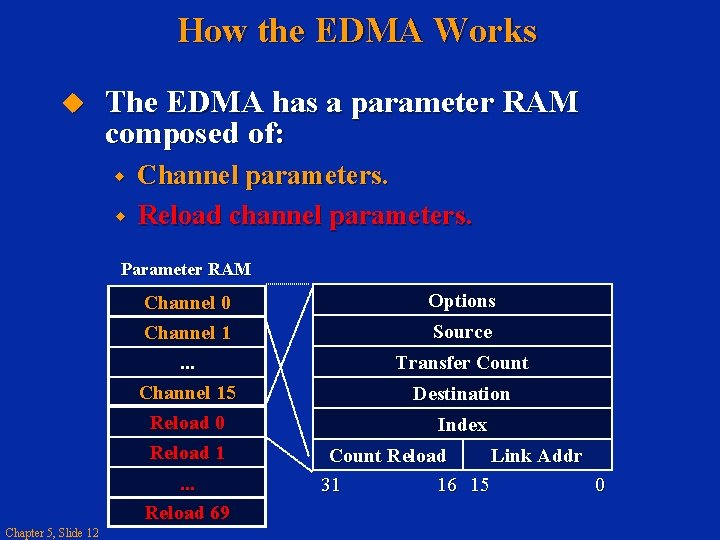
How the EDMA Works The EDMA has a parameter RAM composed of: Channel parameters. Reload channel parameters. Parameter RAM Channel 0 Channel 1 Options . . . Channel 15 Transfer Count Reload 0 Reload 1 Index . . . Reload 69 Chapter 5, Slide 12 Source Destination Count Reload Link Addr 31 16 15 0

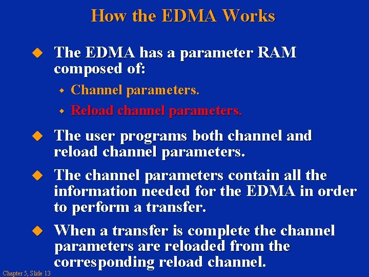
How the EDMA Works The EDMA has a parameter RAM composed of: Chapter 5, Slide 13 Channel parameters. Reload channel parameters. The user programs both channel and reload channel parameters. The channel parameters contain all the information needed for the EDMA in order to perform a transfer. When a transfer is complete the channel parameters are reloaded from the corresponding reload channel.

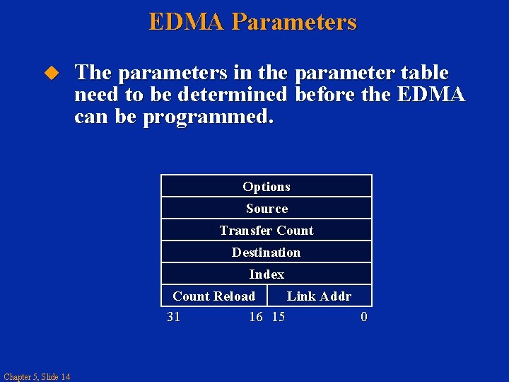
EDMA Parameters The parameters in the parameter table need to be determined before the EDMA can be programmed. Options Source Transfer Count Destination Index Count Reload Link Addr 31 16 15 0 Chapter 5, Slide 14

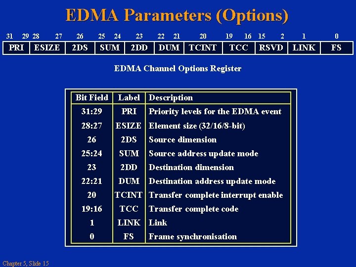
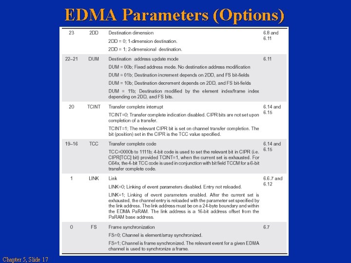
EDMA Parameters (Options) 31 29 28 PRI 27 ESIZE 26 25 2 DS 24 SUM 23 2 DD 22 21 DUM 20 TCINT 19 16 15 TCC 2 RSVD LINK EDMA Channel Options Register Bit Field 31: 29 28: 27 Priority levels for the EDMA event ESIZE Element size (32/16/8 -bit) 26 2 DS Source dimension 25: 24 SUM Source address update mode 23 2 DD Destination dimension 22: 21 DUM Destination address update mode 20 TCINT Transfer complete interrupt enable 19: 16 1 0 Chapter 5, Slide 15 Label Description PRI TCC Transfer complete code LINK Link FS Frame synchronisation 1 0 FS

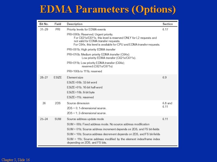
EDMA Parameters (Options) Chapter 5, Slide 16

EDMA Parameters (Options) Chapter 5, Slide 17

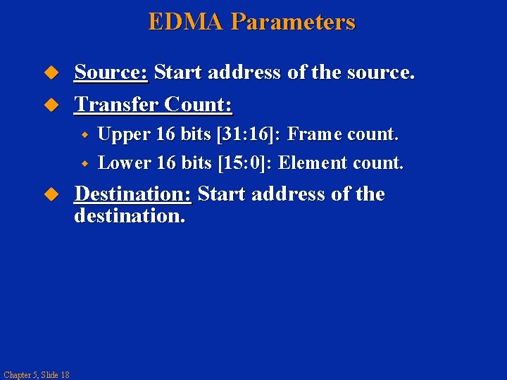
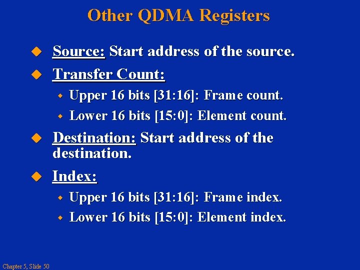
EDMA Parameters Source: Start address of the source. Transfer Count: Chapter 5, Slide 18 Upper 16 bits [31: 16]: Frame count. Lower 16 bits [15: 0]: Element count. Destination: Start address of the destination.
![EDMA Parameters Index Chapter 5 Slide 19 Upper 16 bits 31 16 Frame index EDMA Parameters Index: Chapter 5, Slide 19 Upper 16 bits [31: 16]: Frame index.](https://slidetodoc.com/presentation_image_h/f88ce128b28b152ae6af0e7507e0cc61/image-19.jpg)
EDMA Parameters Index: Chapter 5, Slide 19 Upper 16 bits [31: 16]: Frame index. Lower 16 bits [15: 0]: Element index. Count reload: Value to be reloaded into the element count when a frame is complete (only used in 1 -D mode). Link address: Specifies the address from where the parameters are reloaded. The 16 -bit value is added to 0 x 01 A 0 xxxx to form the 32 -bit address.

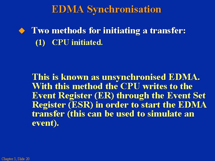
EDMA Synchronisation Two methods for initiating a transfer: (1) CPU initiated. This is known as unsynchronised EDMA. With this method the CPU writes to the Event Register (ER) through the Event Set Register (ESR) in order to start the EDMA transfer (this can be used to simulate an event). Chapter 5, Slide 20

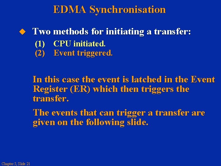
EDMA Synchronisation Two methods for initiating a transfer: (1) CPU initiated. (2) Event triggered. In this case the event is latched in the Event Register (ER) which then triggers the transfer. The events that can trigger a transfer are given on the following slide. Chapter 5, Slide 21

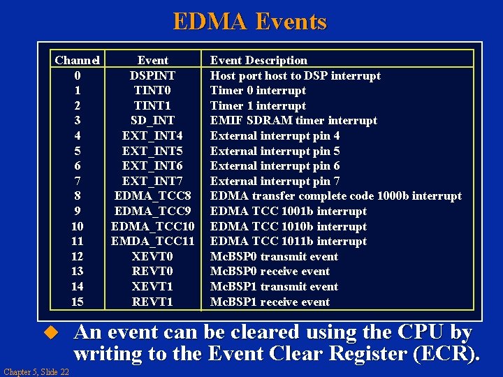
EDMA Events Channel Event 0 DSPINT 1 TINT 0 2 TINT 1 3 SD_INT 4 EXT_INT 4 5 EXT_INT 5 6 EXT_INT 6 7 EXT_INT 7 8 EDMA_TCC 8 9 EDMA_TCC 9 10 EDMA_TCC 10 11 EMDA_TCC 11 12 XEVT 0 13 REVT 0 14 XEVT 1 15 REVT 1 Chapter 5, Slide 22 Event Description Host port host to DSP interrupt Timer 0 interrupt Timer 1 interrupt EMIF SDRAM timer interrupt External interrupt pin 4 External interrupt pin 5 External interrupt pin 6 External interrupt pin 7 EDMA transfer complete code 1000 b interrupt EDMA TCC 1001 b interrupt EDMA TCC 1010 b interrupt EDMA TCC 1011 b interrupt Mc. BSP 0 transmit event Mc. BSP 0 receive event Mc. BSP 1 transmit event Mc. BSP 1 receive event An event can be cleared using the CPU by writing to the Event Clear Register (ECR).

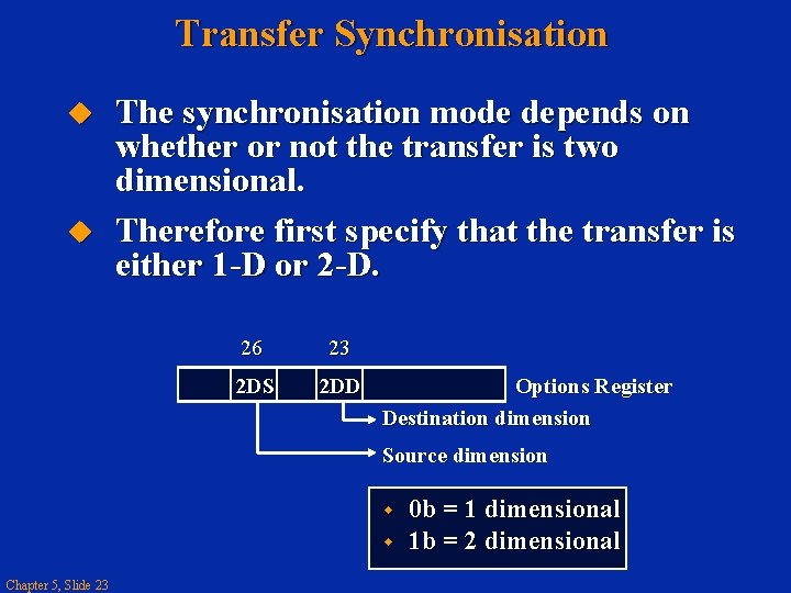
Transfer Synchronisation The synchronisation mode depends on whether or not the transfer is two dimensional. Therefore first specify that the transfer is either 1 -D or 2 -D. 26 23 2 DS 2 DD Options Register Destination dimension Source dimension Chapter 5, Slide 23 0 b = 1 dimensional 1 b = 2 dimensional

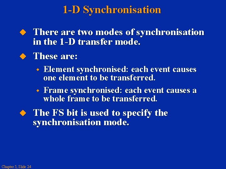
1 -D Synchronisation There are two modes of synchronisation in the 1 -D transfer mode. These are: Chapter 5, Slide 24 Element synchronised: each event causes one element to be transferred. Frame synchronised: each event causes a whole frame to be transferred. The FS bit is used to specify the synchronisation mode.

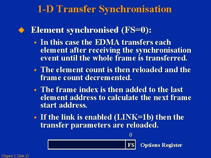
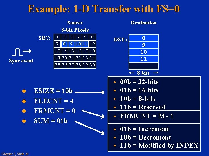
1 -D Transfer Synchronisation Element synchronised (FS=0): In this case the EDMA transfers each element after receiving the synchronisation event until the whole frame is transferred. The element count is then reloaded and the frame count decremented. The frame index is then added to the last element address to calculate the next frame start address. If the link is enabled (LINK=1 b) then the transfer parameters are reloaded. 0 FS Options Register Chapter 5, Slide 25

Example: 1 -D Transfer with FS=0 Source Destination 8 -bit Pixels SRC: 1 2 3 4 5 6 7 8 9 10 11 12 13 14 15 16 17 18 Sync event DST: 19 20 21 22 23 24 25 26 27 28 29 30 8 9 10 11 8 bits ESIZE = 10 b ELECNT = 4 FRMCNT = 0 SUM = 01 b Chapter 5, Slide 26 00 b = 32 -bits 01 b = 16 -bits 10 b = 8 -bits 11 b = Reserved FRMCNT = M - 1 00 b = Fixed 01 b = Increment 10 b = Decrement 11 b = Modified by INDEX

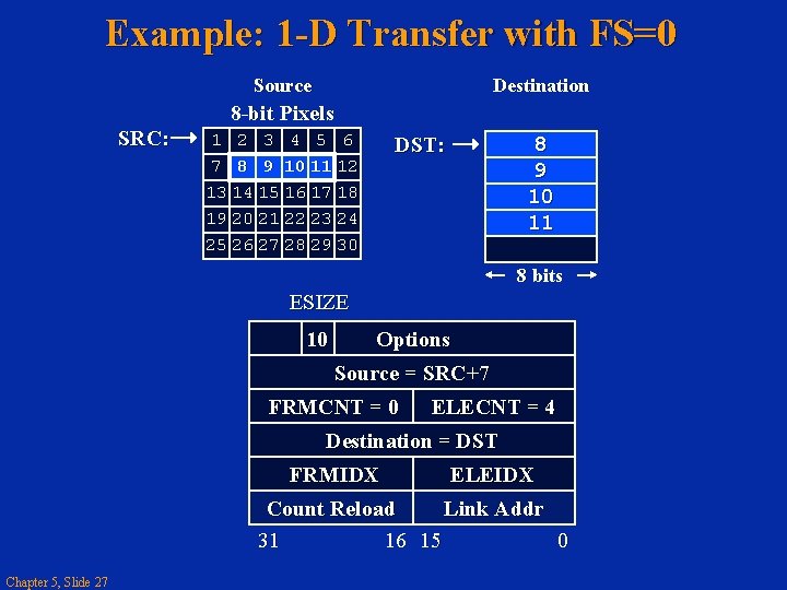
Example: 1 -D Transfer with FS=0 Source Destination 8 -bit Pixels SRC: 1 2 3 4 5 6 7 8 9 10 11 12 13 14 15 16 17 18 8 9 10 11 DST: 19 20 21 22 23 24 25 26 27 28 29 30 8 bits ESIZE 10 Options Source = SRC+7 FRMCNT = 0 ELECNT = 4 Destination = DST FRMIDX ELEIDX Count Reload Link Addr 31 16 15 0 Chapter 5, Slide 27

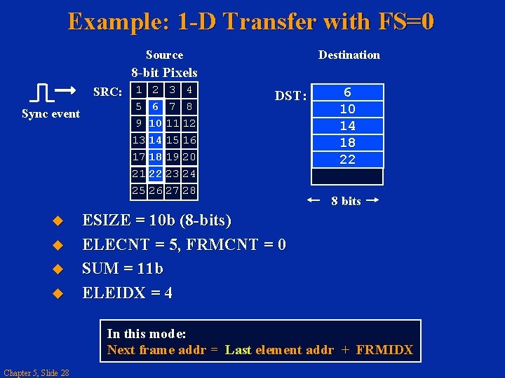
Example: 1 -D Transfer with FS=0 Source Destination 8 -bit Pixels SRC: 1 2 3 4 Sync event 5 6 7 8 9 10 11 12 13 14 15 16 DST: 17 18 19 20 21 22 23 24 25 26 27 28 6 10 14 18 22 8 bits ESIZE = 10 b (8 -bits) ELECNT = 5, FRMCNT = 0 SUM = 11 b ELEIDX = 4 In this mode: Next frame addr = Last element addr + FRMIDX Chapter 5, Slide 28

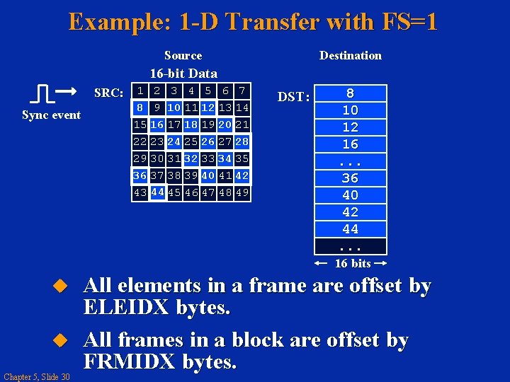
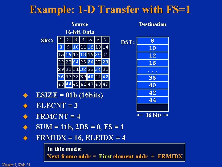
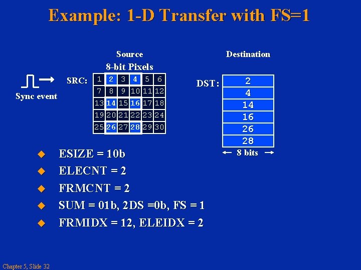
1 -D Transfer Synchronisation Frame synchronised (FS=1): Chapter 5, Slide 29 In this case the EDMA transfers a whole frame after receiving the synchronisation event. In this mode the frame index no longer represents the difference between the address of the last element of the frame and the start address of the next frame. The frame index is added to the start address of the frame to derive the start address of the next frame. See the example on the following slide.

Example: 1 -D Transfer with FS=1 Source Destination 16 -bit Data SRC: 1 2 3 4 5 6 7 Sync event 8 9 10 11 12 13 14 15 16 17 18 19 20 21 22 23 24 25 26 27 28 29 30 31 32 33 34 35 36 37 38 39 40 41 42 43 44 44 45 46 47 48 49 DST: 8 10 12 16. . . 36 40 42 44. . . 16 bits Chapter 5, Slide 30 All elements in a frame are offset by ELEIDX bytes. All frames in a block are offset by FRMIDX bytes.

Example: 1 -D Transfer with FS=1 Source Destination 16 -bit Data SRC: 1 2 3 4 5 6 7 8 9 10 11 12 13 14 15 16 17 18 19 20 21 22 23 24 25 26 27 28 DST: 29 30 31 32 33 34 35 36 37 38 39 40 41 42 43 44 44 45 46 47 48 49 ESIZE = 01 b (16 bits) ELECNT = 3 FRMCNT = 4 SUM = 11 b, 2 DS = 0, FS = 1 FRMIDX = 16, ELEIDX = 4 8 10 12 16. . . 36 40 42 44 16 bits In this mode: Next frame addr = First element addr + FRMIDX Chapter 5, Slide 31

Example: 1 -D Transfer with FS=1 Source Destination 8 -bit Pixels SRC: 1 2 3 4 5 6 Sync event 7 8 9 10 11 12 13 14 15 16 17 18 19 20 21 22 23 24 DST: 25 26 27 28 29 30 Chapter 5, Slide 32 ESIZE = 10 b ELECNT = 2 FRMCNT = 2 SUM = 01 b, 2 DS =0 b, FS = 1 FRMIDX = 12, ELEIDX = 2 2 4 14 16 26 28 8 bits

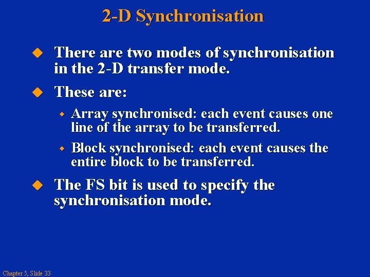
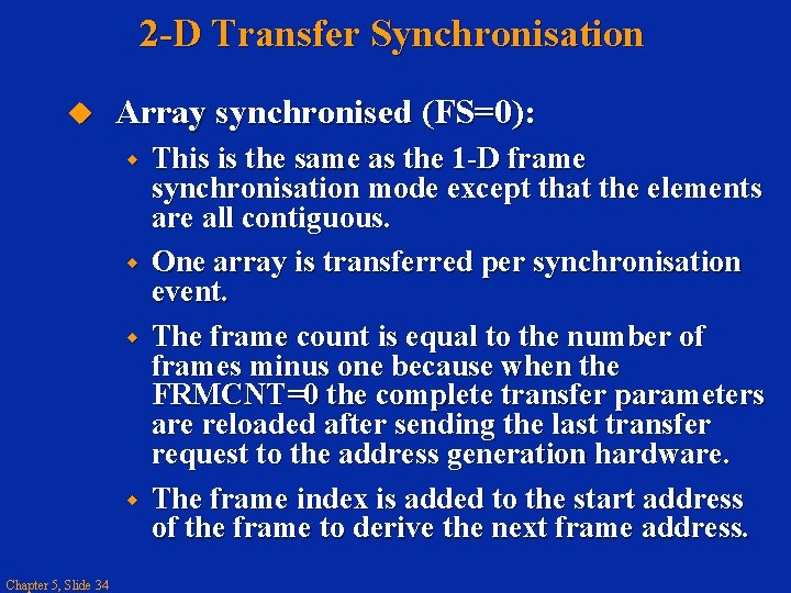
2 -D Synchronisation There are two modes of synchronisation in the 2 -D transfer mode. These are: Chapter 5, Slide 33 Array synchronised: each event causes one line of the array to be transferred. Block synchronised: each event causes the entire block to be transferred. The FS bit is used to specify the synchronisation mode.

2 -D Transfer Synchronisation Array synchronised (FS=0): Chapter 5, Slide 34 This is the same as the 1 -D frame synchronisation mode except that the elements are all contiguous. One array is transferred per synchronisation event. The frame count is equal to the number of frames minus one because when the FRMCNT=0 the complete transfer parameters are reloaded after sending the last transfer request to the address generation hardware. The frame index is added to the start address of the frame to derive the next frame address.

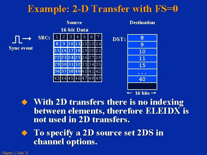
Example: 2 -D Transfer with FS=0 Source Destination 16 -bit Data SRC: 1 2 3 4 5 6 7 Sync event 8 9 10 11 12 13 14 15 16 17 18 19 20 21 22 23 24 25 26 27 28 29 30 31 32 33 34 35 36 37 38 39 40 40 41 42 43 44 45 46 47 48 49 DST: 8 9 10 11 15. . . 40 16 bits Chapter 5, Slide 35 With 2 D transfers there is no indexing between elements, therefore ELEIDX is not used in 2 D transfers. To specify a 2 D source set 2 DS in channel options.

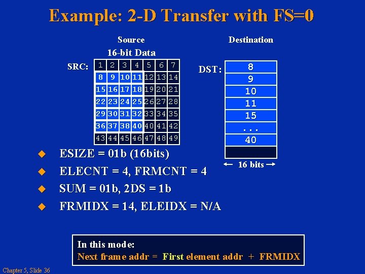
Example: 2 -D Transfer with FS=0 Source Destination 16 -bit Data SRC: 1 2 3 4 5 6 7 8 9 10 11 12 13 14 15 16 17 18 19 20 21 22 23 24 25 26 27 28 DST: 29 30 31 32 33 34 35 36 37 38 39 40 40 41 42 43 44 45 46 47 48 49 ESIZE = 01 b (16 bits) ELECNT = 4, FRMCNT = 4 SUM = 01 b, 2 DS = 1 b FRMIDX = 14, ELEIDX = N/A 8 9 10 11 15. . . 40 16 bits In this mode: Next frame addr = First element addr + FRMIDX Chapter 5, Slide 36

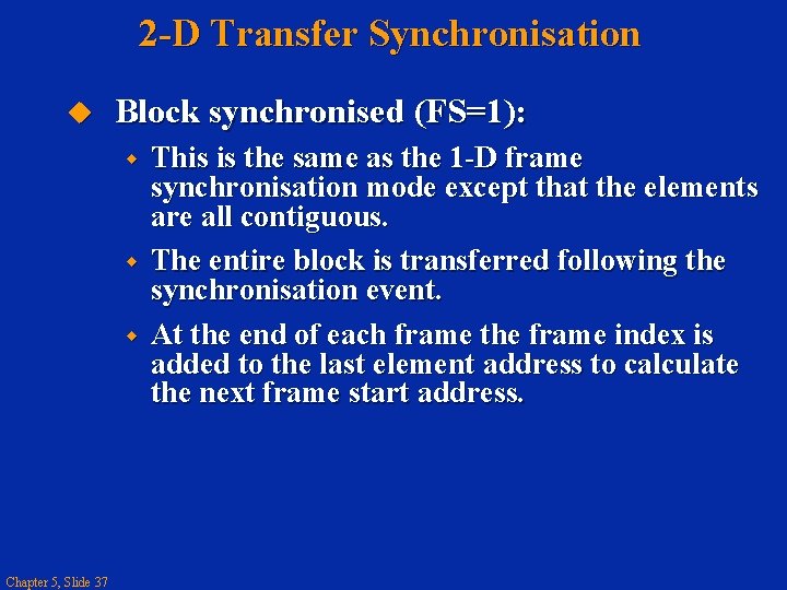
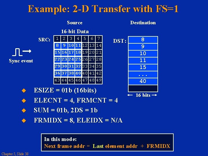
2 -D Transfer Synchronisation Block synchronised (FS=1): Chapter 5, Slide 37 This is the same as the 1 -D frame synchronisation mode except that the elements are all contiguous. The entire block is transferred following the synchronisation event. At the end of each frame the frame index is added to the last element address to calculate the next frame start address.

Example: 2 -D Transfer with FS=1 Source Destination 16 -bit Data SRC: 1 2 3 4 5 6 7 Sync event 8 9 10 11 12 13 14 15 16 17 18 19 20 21 22 23 24 25 26 27 28 DST: 29 30 31 32 33 34 35 36 37 38 39 40 40 41 42 43 44 45 46 47 48 49 ESIZE = 01 b (16 bits) ELECNT = 4, FRMCNT = 4 SUM = 01 b, 2 DS = 1 b FRMIDX = 8, ELEIDX = N/A 8 9 10 11 15. . . 40 16 bits In this mode: Next frame addr = Last element addr + FRMIDX Chapter 5, Slide 38

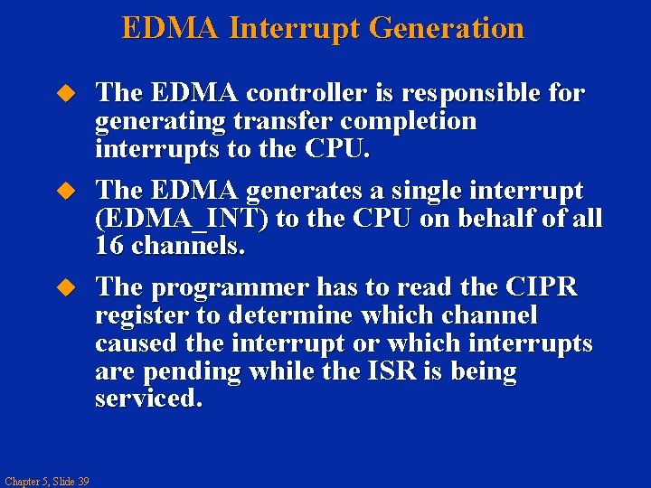
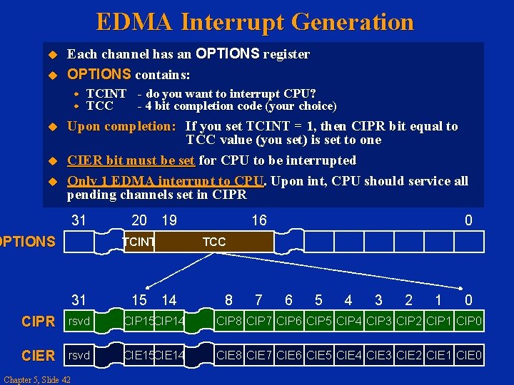
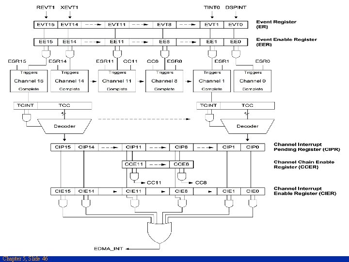
EDMA Interrupt Generation Chapter 5, Slide 39 The EDMA controller is responsible for generating transfer completion interrupts to the CPU. The EDMA generates a single interrupt (EDMA_INT) to the CPU on behalf of all 16 channels. The programmer has to read the CIPR register to determine which channel caused the interrupt or which interrupts are pending while the ISR is being serviced.

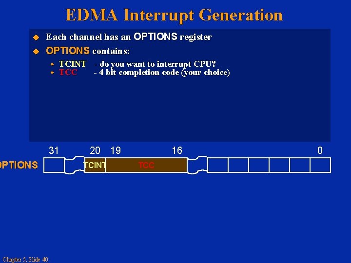
EDMA Interrupt Generation Each channel has an OPTIONS register OPTIONS contains: TCINT - do you want to interrupt CPU? TCC - 4 bit completion code (your choice) 31 OPTIONS Chapter 5, Slide 40 20 19 TCINT 16 TCC 0

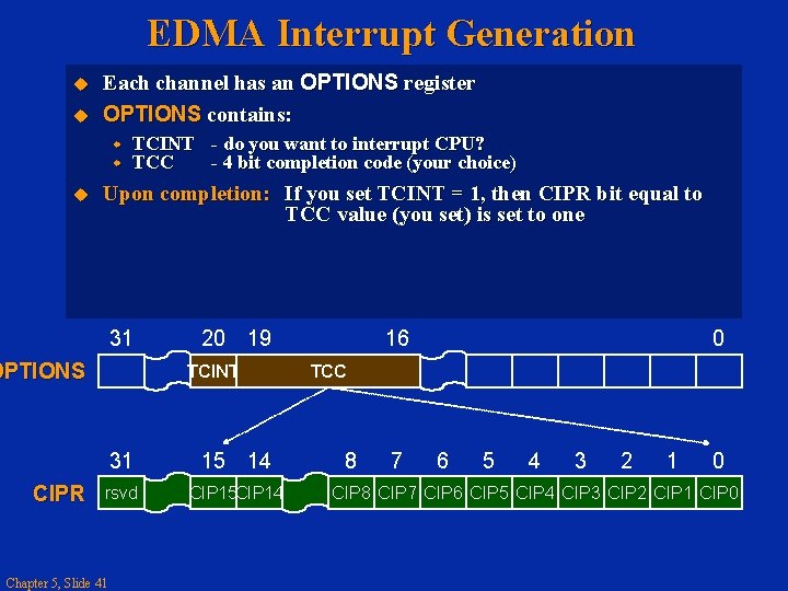
EDMA Interrupt Generation Each channel has an OPTIONS register OPTIONS contains: TCINT - do you want to interrupt CPU? TCC - 4 bit completion code (your choice) Upon completion: If you set TCINT = 1, then CIPR bit equal to TCC value (you set) is set to one 31 OPTIONS CIPR 20 19 TCINT 31 15 14 rsvd CIP 15 CIP 14 Chapter 5, Slide 41 16 0 TCC 8 7 6 5 4 3 2 1 0 CIP 8 CIP 7 CIP 6 CIP 5 CIP 4 CIP 3 CIP 2 CIP 1 CIP 0

EDMA Interrupt Generation Each channel has an OPTIONS register OPTIONS contains: TCINT - do you want to interrupt CPU? TCC - 4 bit completion code (your choice) Upon completion: If you set TCINT = 1, then CIPR bit equal to TCC value (you set) is set to one CIER bit must be set for CPU to be interrupted Only 1 EDMA interrupt to CPU. Upon int, CPU should service all pending channels set in CIPR 31 OPTIONS 20 19 TCINT 16 0 TCC 31 15 14 CIPR rsvd CIP 15 CIP 14 CIP 8 CIP 7 CIP 6 CIP 5 CIP 4 CIP 3 CIP 2 CIP 1 CIP 0 CIER rsvd CIE 15 CIE 14 CIE 8 CIE 7 CIE 6 CIE 5 CIE 4 CIE 3 CIE 2 CIE 1 CIE 0 Chapter 5, Slide 42 8 7 6 5 4 3 2 1 0

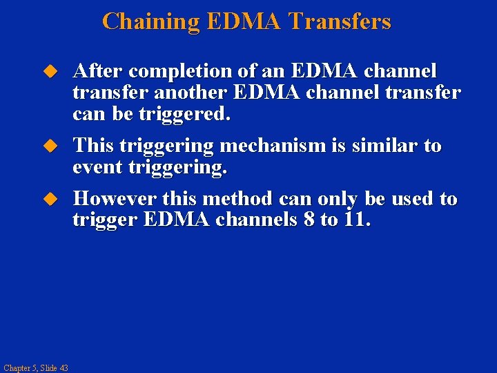
Chaining EDMA Transfers Chapter 5, Slide 43 After completion of an EDMA channel transfer another EDMA channel transfer can be triggered. This triggering mechanism is similar to event triggering. However this method can only be used to trigger EDMA channels 8 to 11.

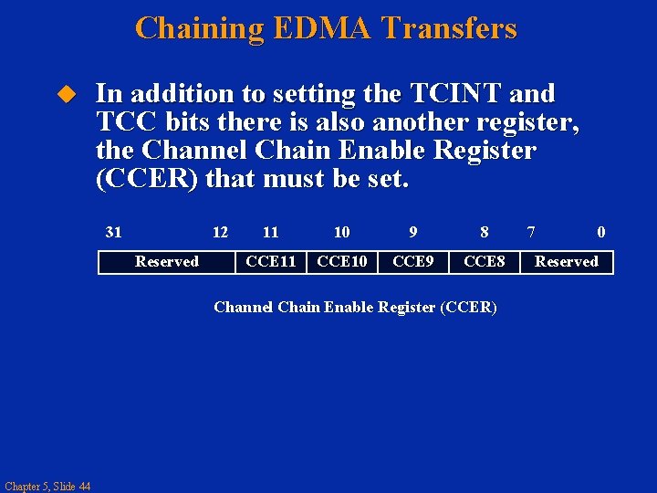
Chaining EDMA Transfers In addition to setting the TCINT and TCC bits there is also another register, the Channel Chain Enable Register (CCER) that must be set. 31 12 Reserved 11 10 9 8 CCE 11 CCE 10 CCE 9 CCE 8 Channel Chain Enable Register (CCER) Chapter 5, Slide 44 7 0 Reserved

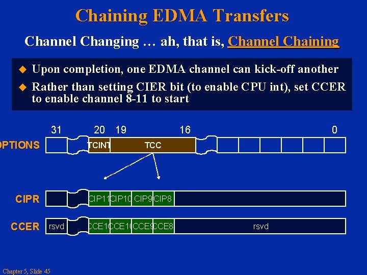
Chaining EDMA Transfers Channel Changing … ah, that is, Channel Chaining Upon completion, one EDMA channel can kick-off another Rather than setting CIER bit (to enable CPU int), set CCER to enable channel 8 -11 to start 31 OPTIONS TCINT CIPR CCER 20 19 16 0 TCC CIP 11 CIP 10 CIP 9 CIP 8 rsvd Chapter 5, Slide 45 CCE 11 CCE 10 CCE 9 CCE 8 rsvd

EDMA Interrupt Generation Chapter 5, Slide 46

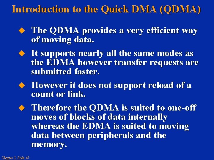
Introduction to the Quick DMA (QDMA) Chapter 5, Slide 47 The QDMA provides a very efficient way of moving data. It supports nearly all the same modes as the EDMA however transfer requests are submitted faster. However it does not support reload of a count or link. Therefore the QDMA is suited to one-off moves of blocks of data internally whereas the EDMA is suited to moving data between peripherals and the memory.

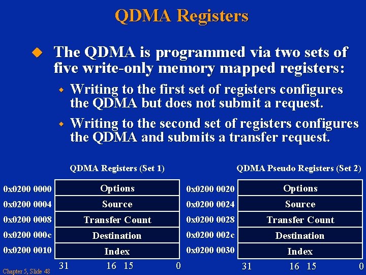
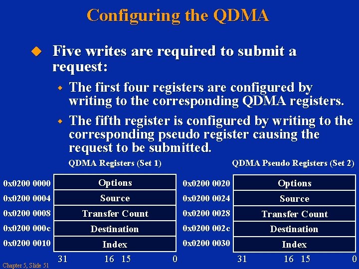
QDMA Registers The QDMA is programmed via two sets of five write-only memory mapped registers: Writing to the first set of registers configures the QDMA but does not submit a request. Writing to the second set of registers configures the QDMA and submits a transfer request. QDMA Registers (Set 1) QDMA Pseudo Registers (Set 2) 0 x 0200 0000 Options 0 x 0200 0020 Options 0 x 0200 0004 Source 0 x 0200 0024 Source 0 x 0200 0008 Transfer Count 0 x 0200 0028 Transfer Count 0 x 0200 000 c Destination 0 x 0200 002 c Destination 0 x 0200 0010 Index 16 15 0 x 0200 0030 Index 16 15 Chapter 5, Slide 48 31 0

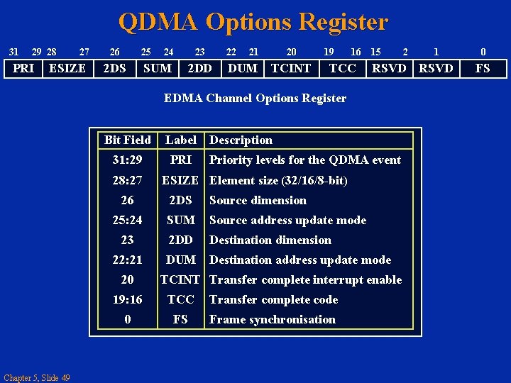
QDMA Options Register 31 29 28 PRI 27 ESIZE 26 25 2 DS 24 SUM 23 22 2 DD 21 DUM 20 TCINT 19 16 15 TCC 31: 29 28: 27 Chapter 5, Slide 49 Label Description PRI Priority levels for the QDMA event ESIZE Element size (32/16/8 -bit) 26 2 DS Source dimension 25: 24 SUM Source address update mode 23 2 DD Destination dimension 22: 21 DUM Destination address update mode 20 TCINT Transfer complete interrupt enable 19: 16 TCC Transfer complete code 0 FS Frame synchronisation 1 RSVD EDMA Channel Options Register Bit Field 2 0 FS

Other QDMA Registers Source: Start address of the source. Transfer Count: Destination: Start address of the destination. Index: Chapter 5, Slide 50 Upper 16 bits [31: 16]: Frame count. Lower 16 bits [15: 0]: Element count. Upper 16 bits [31: 16]: Frame index. Lower 16 bits [15: 0]: Element index.

Configuring the QDMA Five writes are required to submit a request: The first four registers are configured by writing to the corresponding QDMA registers. The fifth register is configured by writing to the corresponding pseudo register causing the request to be submitted. QDMA Registers (Set 1) QDMA Pseudo Registers (Set 2) 0 x 0200 0000 Options 0 x 0200 0020 Options 0 x 0200 0004 Source 0 x 0200 0024 Source 0 x 0200 0008 Transfer Count 0 x 0200 0028 Transfer Count 0 x 0200 000 c Destination 0 x 0200 002 c Destination 0 x 0200 0010 Index 16 15 0 x 0200 0030 Index 16 15 Chapter 5, Slide 51 31 0

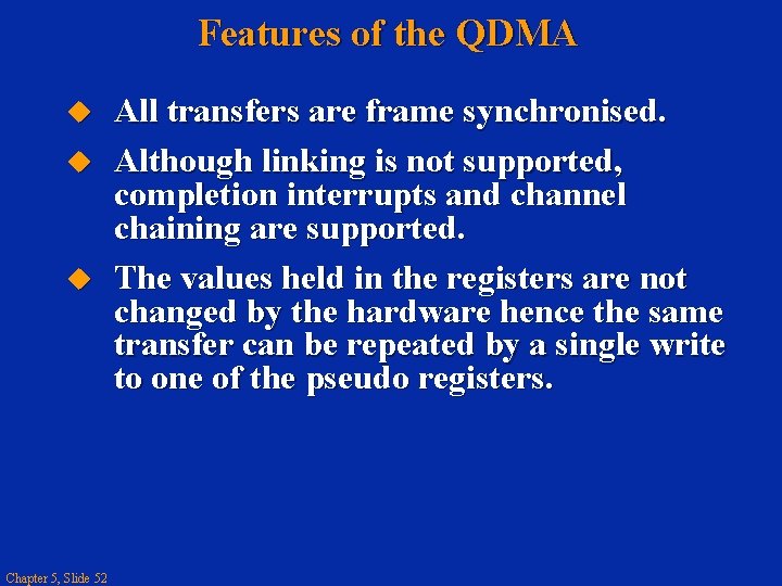
Features of the QDMA Chapter 5, Slide 52 All transfers are frame synchronised. Although linking is not supported, completion interrupts and channel chaining are supported. The values held in the registers are not changed by the hardware hence the same transfer can be repeated by a single write to one of the pseudo registers.

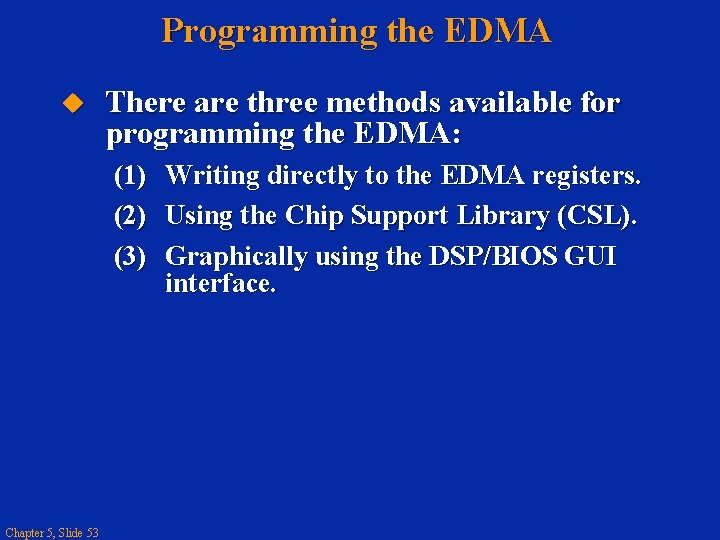
Programming the EDMA There are three methods available for programming the EDMA: (1) Writing directly to the EDMA registers. (2) Using the Chip Support Library (CSL). (3) Graphically using the DSP/BIOS GUI interface. Chapter 5, Slide 53

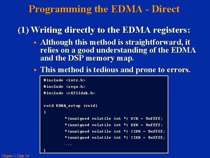
Programming the EDMA - Direct (1) Writing directly to the EDMA registers: Although this method is straightforward, it relies on a good understanding of the EDMA and the DSP memory map. This method is tedious and prone to errors. #include <intr. h> #include <regs. h> #include <c 6211 dsk. h> void EDMA_setup (void) { *(unsigned volatile int *) ECR = 0 xffff; *(unsigned volatile int *) EER = 0 xffff; *(unsigned volatile int *) CIPR = 0 xffff; *(unsigned volatile int *) CIER = 0 xffff; . . . } Chapter 5, Slide 54

Programming the EDMA - CSL (2) Using the Chip Support Library: Chapter 5, Slide 55 The CSL provides a C language interface for configuring and controlling the on-chip peripherals, in this case the EDMA. The library is modular with each module corresponding to a specific peripheral. This has the advantage of reducing the code size. Some modules rely on other modules also being included, for example the IRQ module is required when using the EDMA module.

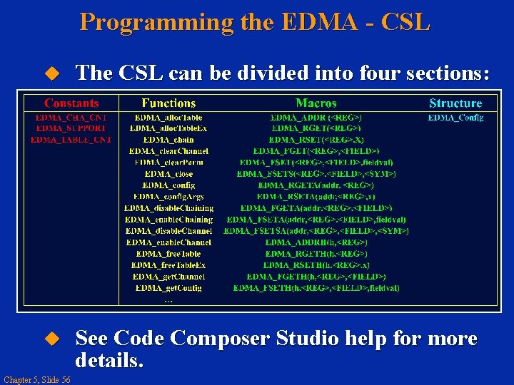
Programming the EDMA - CSL The CSL can be divided into four sections: See Code Composer Studio help for more details. Chapter 5, Slide 56

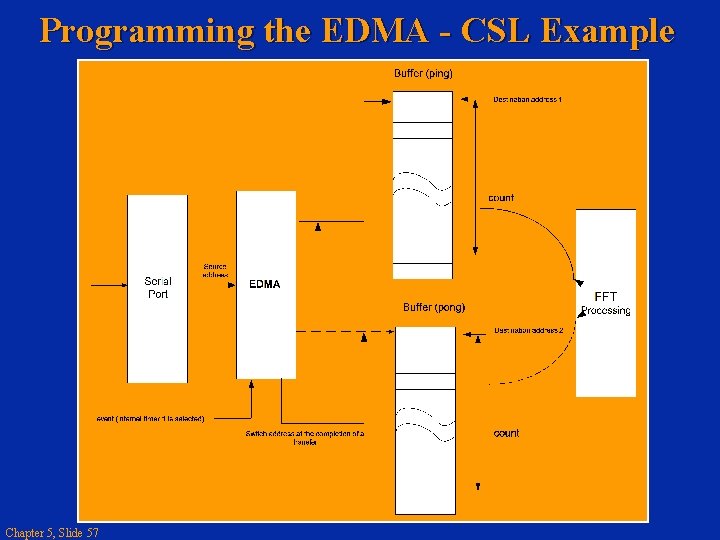
Programming the EDMA - CSL Example Chapter 5, Slide 57

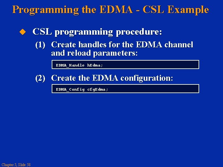
Programming the EDMA - CSL Example CSL programming procedure: (1) Create handles for the EDMA channel and reload parameters: EDMA_Handle h. Edma; (2) Create the EDMA configuration: EDMA_Config cfg. Edma; Chapter 5, Slide 58

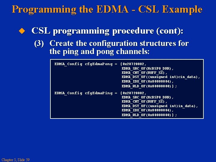
Programming the EDMA - CSL Example CSL programming procedure (cont): (3) Create the configuration structures for the ping and pong channels: EDMA_Config cfg. Edma. Pong = {0 x 28720002, EDMA_SRC_OF(Mc. BSP 0_DRR), EDMA_CNT_OF(BUFF_SZ), EDMA_DST_OF((unsigned int)cin_data), EDMA_IDX_OF(0 x 00000004), EDMA_RLD_OF(0 x 0000) }; EDMA_Config cfg. Edma. Ping = {0 x 28720002, EDMA_SRC_OF(Mc. BSP 0_DRR), EDMA_CNT_OF(BUFF_SZ), EDMA_DST_OF((unsigned int)in_data), EDMA_IDX_OF(0 x 00000004), EDMA_RLD_OF(0 x 0000) }; Chapter 5, Slide 59

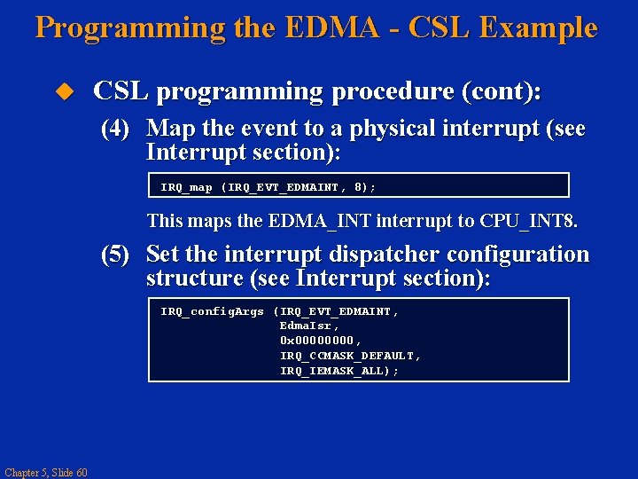
Programming the EDMA - CSL Example CSL programming procedure (cont): (4) Map the event to a physical interrupt (see Interrupt section): IRQ_map (IRQ_EVT_EDMAINT, 8); This maps the EDMA_INT interrupt to CPU_INT 8. (5) Set the interrupt dispatcher configuration structure (see Interrupt section): IRQ_config. Args (IRQ_EVT_EDMAINT, Edma. Isr, 0 x 0000, IRQ_CCMASK_DEFAULT, IRQ_IEMASK_ALL); Chapter 5, Slide 60

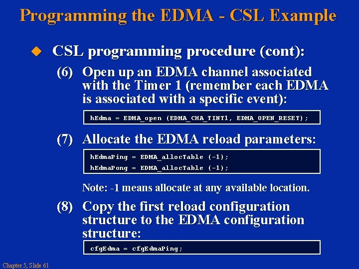
Programming the EDMA - CSL Example CSL programming procedure (cont): (6) Open up an EDMA channel associated with the Timer 1 (remember each EDMA is associated with a specific event): h. Edma = EDMA_open (EDMA_CHA_TINT 1, EDMA_OPEN_RESET); (7) Allocate the EDMA reload parameters: h. Edma. Ping = EDMA_alloc. Table (-1); h. Edma. Pong = EDMA_alloc. Table (-1); Note: -1 means allocate at any available location. (8) Copy the first reload configuration structure to the EDMA configuration structure: cfg. Edma = cfg. Edma. Ping; Chapter 5, Slide 61

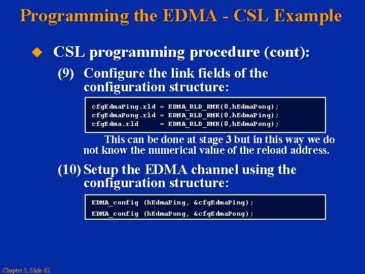
Programming the EDMA - CSL Example CSL programming procedure (cont): (9) Configure the link fields of the configuration structure: cfg. Edma. Ping. rld cfg. Edma. Pong. rld cfg. Edma. rld = = = EDMA_RLD_RMK(0, h. Edma. Pong); EDMA_RLD_RMK(0, h. Edma. Ping); EDMA_RLD_RMK(0, h. Edma. Pong); This can be done at stage 3 but in this way we do not know the numerical value of the reload address. (10) Setup the EDMA channel using the configuration structure: EDMA_config (h. Edma. Ping, &cfg. Edma. Ping); EDMA_config (h. Edma. Pong, &cfg. Edma. Pong); Chapter 5, Slide 62

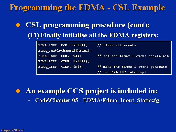
Programming the EDMA - CSL Example CSL programming procedure (cont): (11) Finally initialise all the EDMA registers: EDMA_RSET (ECR, 0 xffff); // clear all events EDMA_enable. Channel(h. Edma); EDMA_RSET (EER, 0 x 4); // set the timer 1 event enable bit EDMA_RSET (CIPR, 0 xffff); EDMA_RSET (CIER, 0 x 4); // make the timer 1 event generate // an EDMA_INT interrupt An example CCS project is included in: Chapter 5, Slide 63 CodeChapter 05 - EDMAEdma_Inout_Staticcfg

Programming the EDMA - DSP/BIOS GUI (3) DSP/BIOS GUI Interface Chapter 5, Slide 64 With this method the configuration structure is created graphically and the setup code is generated automatically.

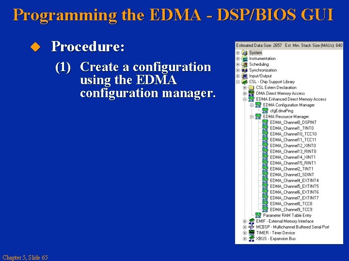
Programming the EDMA - DSP/BIOS GUI Procedure: (1) Create a configuration using the EDMA configuration manager. Chapter 5, Slide 65

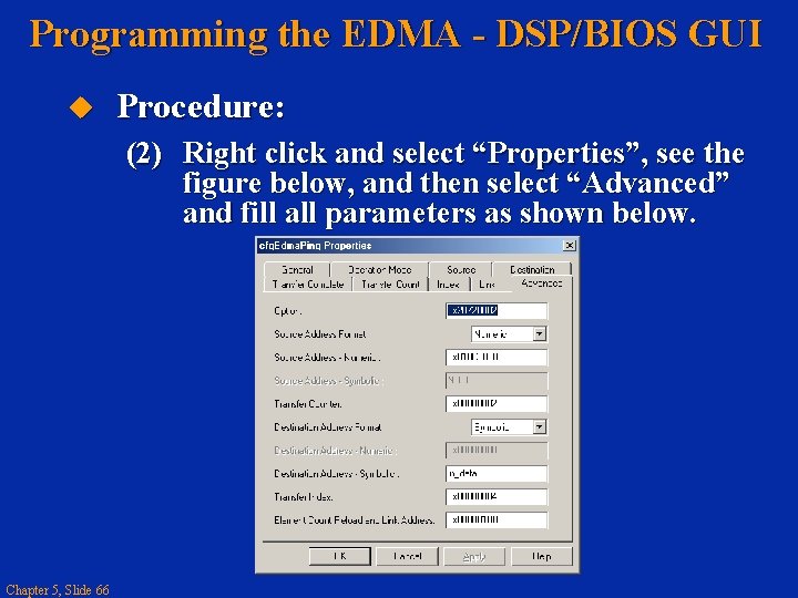
Programming the EDMA - DSP/BIOS GUI Procedure: (2) Right click and select “Properties”, see the figure below, and then select “Advanced” and fill all parameters as shown below. Chapter 5, Slide 66

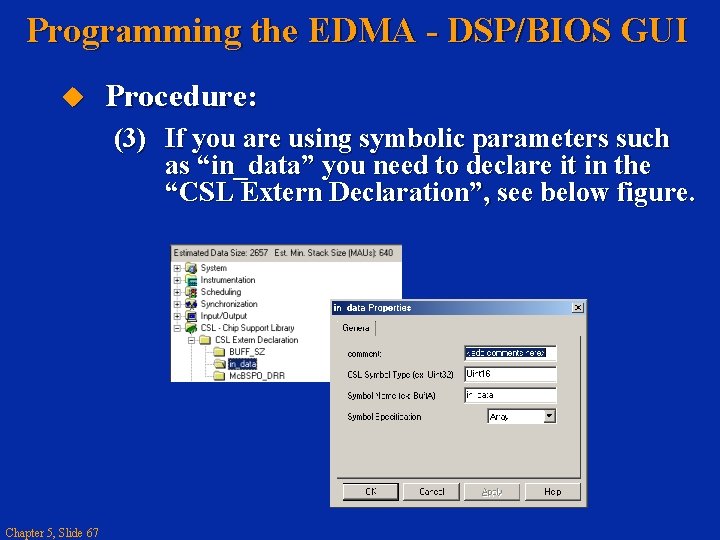
Programming the EDMA - DSP/BIOS GUI Procedure: (3) If you are using symbolic parameters such as “in_data” you need to declare it in the “CSL Extern Declaration”, see below figure. Chapter 5, Slide 67

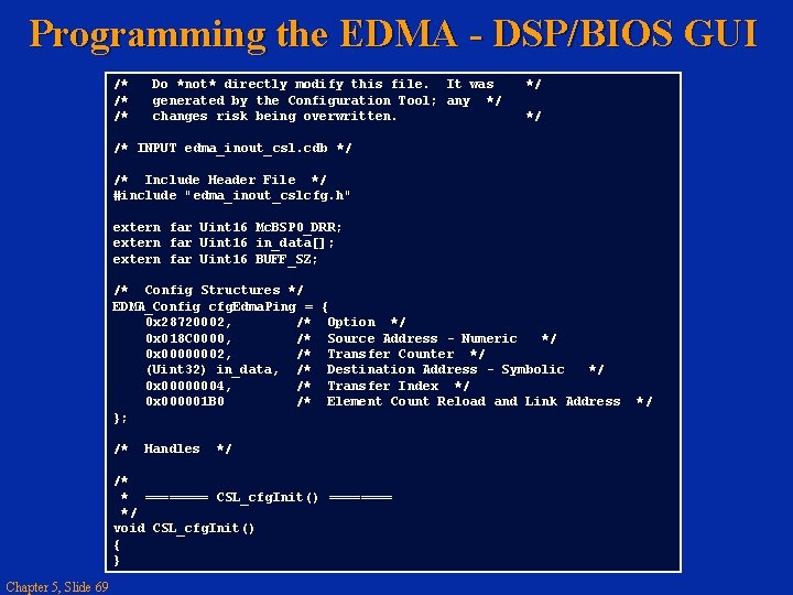
Programming the EDMA - DSP/BIOS GUI Procedure: (4) A file is then generated that contains the configuration code. The file generated for this example is shown on the next slide. Chapter 5, Slide 68

Programming the EDMA - DSP/BIOS GUI /* /* /* Do *not* directly modify this file. It was generated by the Configuration Tool; any */ changes risk being overwritten. */ */ /* INPUT edma_inout_csl. cdb */ /* Include Header File */ #include "edma_inout_cslcfg. h " extern far Uint 16 Mc. BSP 0_DRR; extern far Uint 16 in_data[]; extern far Uint 16 BUFF_SZ; /* Config Structures */ EDMA_Config cfg. Edma. Ping = { 0 x 28720002, /* Option */ 0 x 018 C 0000, /* Source Address - Numeric */ 0 x 00000002, /* Transfer Counter */ (Uint 32) in_data, /* Destination Address - Symbolic */ 0 x 00000004, /* Transfer Index */ 0 x 000001 B 0 /* Element Count Reload and Link Address }; /* Handles */ /* * ==== CSL_cfg. Init() ==== */ void CSL_cfg. Init() { } Chapter 5, Slide 69 */

Chapter 5 Enhanced Direct Memory Access (EDMA) - End -