Chapter 2 Signals and Amplifiers from Microelectronic Circuits
- Slides: 95

Chapter #2: Signals and Amplifiers from Microelectronic Circuits Text by Sedra and Smith Oxford Publishing Oxford University Publishing Microelectronic Circuits by Adel S. Sedra and Kenneth C. Smith (0195323033)

Introduction § IN THIS CHAPTER YOU WILL LEARN § The terminal characteristics of the ideal op-amp. § How to analyze circuits containing op-amps, resistors, and capacitors. § How to use op-amps to design amplifiers having precise characteristics. Oxford University Publishing Microelectronic Circuits by Adel S. Sedra and Kenneth C. Smith (0195323033)

Introduction § IN THIS CHAPTER YOU WILL LEARN § How to design more sophisticated op-amp circuits, including summing amplifiers, instrumentation amplifiers, integrators, and differentiators. § Important non-ideal characteristics of op-amps and how these limit the performance of basic op-amp circuits. Oxford University Publishing Microelectronic Circuits by Adel S. Sedra and Kenneth C. Smith (0195323033)

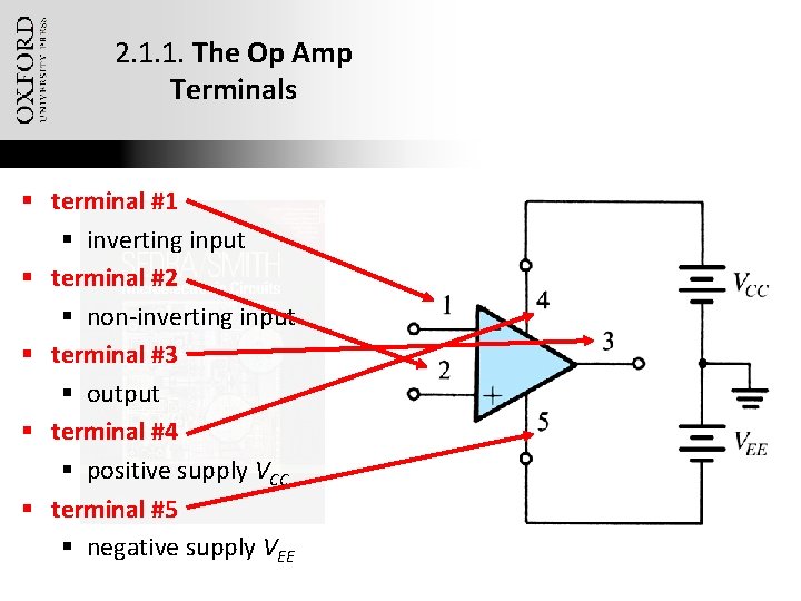
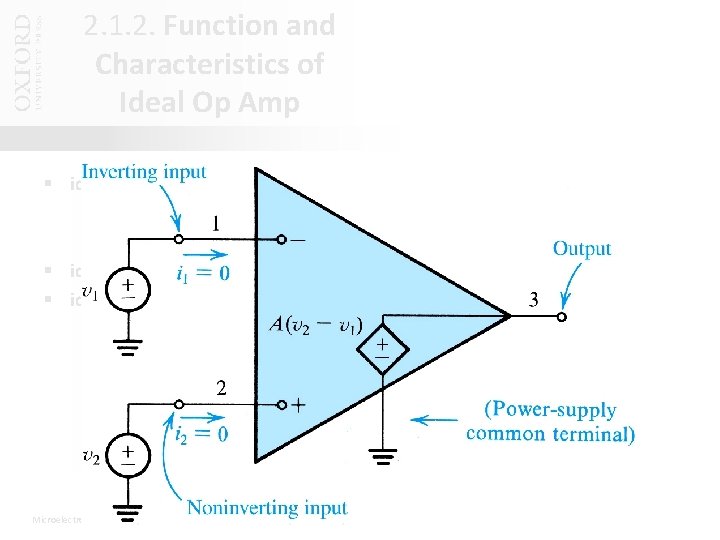
2. 1. 1. The Op Amp Terminals § terminal #1 § inverting input § terminal #2 § non-inverting input § terminal #3 § output § terminal #4 § positive supply VCC § terminal #5 § negative supply VEE Oxford University Publishing Microelectronic Circuits by Adel S. Sedra and Kenneth C. Smith (0195323033)

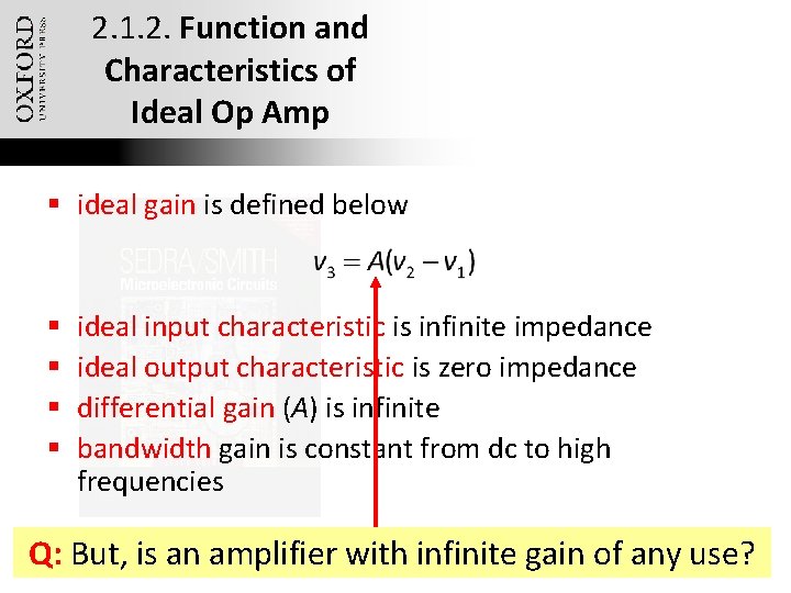
2. 1. 2. Function and Characteristics of Ideal Op Amp § ideal gain is defined below § § ideal input characteristic is infinite impedance ideal output characteristic is zero impedance differential gain (A) is infinite bandwidth gain is constant from dc to high frequencies Q: But, is an amplifier with infinite gain of any use? Oxford University Publishing Microelectronic Circuits by Adel S. Sedra and Kenneth C. Smith (0195323033)

2. 1. 2. Function and Characteristics of Ideal Op Amp § ideal gain: is defined below § ideal input characteristic: infinite impedance § ideal output characteristic: zero impedance Oxford University Publishing Microelectronic Circuits by Adel S. Sedra and Kenneth C. Smith (0195323033)

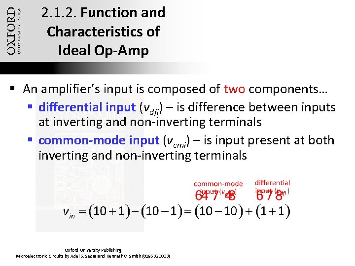
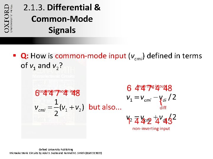
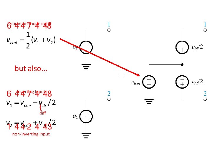
2. 1. 2. Function and Characteristics of Ideal Op-Amp § An amplifier’s input is composed of two components… § differential input (vdfi) – is difference between inputs at inverting and non-inverting terminals § common-mode input (vcmi) – is input present at both inverting and non-inverting terminals Oxford University Publishing Microelectronic Circuits by Adel S. Sedra and Kenneth C. Smith (0195323033)

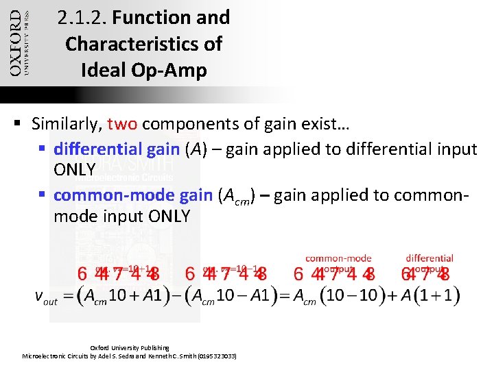
2. 1. 2. Function and Characteristics of Ideal Op-Amp § Similarly, two components of gain exist… § differential gain (A) – gain applied to differential input ONLY § common-mode gain (Acm) – gain applied to commonmode input ONLY Oxford University Publishing Microelectronic Circuits by Adel S. Sedra and Kenneth C. Smith (0195323033)

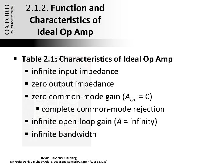
2. 1. 2. Function and Characteristics of Ideal Op Amp § Table 2. 1: Characteristics of Ideal Op Amp § infinite input impedance § zero output impedance § zero common-mode gain (Acm = 0) § complete common-mode rejection § infinite open-loop gain (A = infinity) § infinite bandwidth Oxford University Publishing Microelectronic Circuits by Adel S. Sedra and Kenneth C. Smith (0195323033)

2. 1. 3. Differential & Common-Mode Signals § Q: How is common-mode input (vcmi) defined in terms of v 1 and v 2? Oxford University Publishing Microelectronic Circuits by Adel S. Sedra and Kenneth C. Smith (0195323033)

2. 1. 3. Differential & Common-Mode Signals Oxford University Publishing Microelectronic Circuits by Adel S. Sedra and Kenneth C. Smith (0195323033)

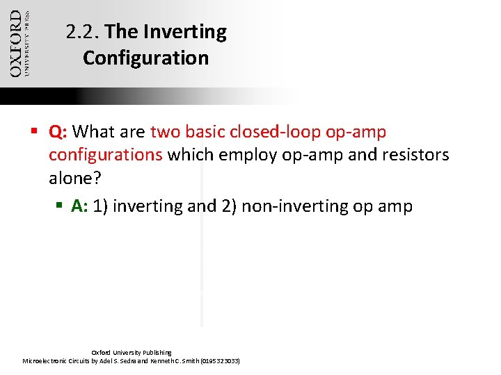
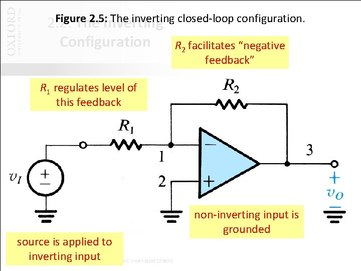
2. 2. The Inverting Configuration § Q: What are two basic closed-loop op-amp configurations which employ op-amp and resistors alone? § A: 1) inverting and 2) non-inverting op amp Oxford University Publishing Microelectronic Circuits by Adel S. Sedra and Kenneth C. Smith (0195323033)

Figure 2. 5: Inverting The inverting closed-loop configuration. 2. 2. The Configuration R 2 facilitates “negative feedback” R 1 regulates level § question: what are twoofbasic closed-loop op amp configurations which this feedback employ op-amp and resistors alone? § answer: inverting and non-inverting op amp § note: here we examine the inverting type source is applied to Oxford University Publishing inverting input Microelectronic Circuits by Adel S. Sedra and Kenneth C. Smith (0195323033) non-inverting input is grounded

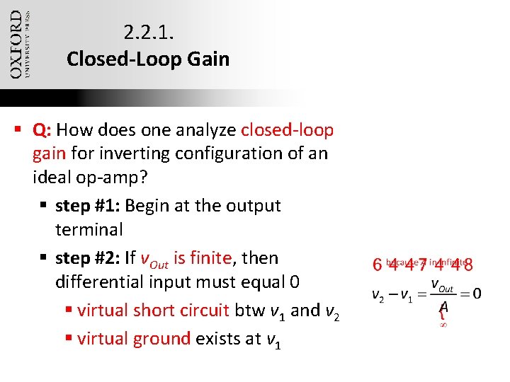
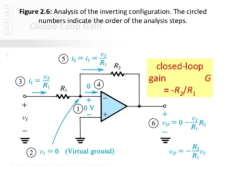
2. 2. 1. Closed-Loop Gain § Q: How does one analyze closed-loop gain for inverting configuration of an ideal op-amp? § step #1: Begin at the output terminal § step #2: If v. Out is finite, then differential input must equal 0 § virtual short circuit btw v 1 and v 2 § virtual ground exists at v 1 Oxford University Publishing Microelectronic Circuits by Adel S. Sedra and Kenneth C. Smith (0195323033)

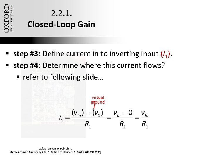
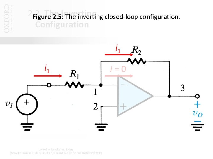
2. 2. 1. Closed-Loop Gain § step #3: Define current in to inverting input (i 1). § step #4: Determine where this current flows? § refer to following slide… Oxford University Publishing Microelectronic Circuits by Adel S. Sedra and Kenneth C. Smith (0195323033)

2. 2. The Figure 2. 5: Inverting The inverting closed-loop configuration. Configuration i 1 § question: what are two basic closed-loop op amp configurations which employ op-amp and resistors alone? i 1 inverting and non-inverting § answer: i =op-amp 0 § note: here we examine the inverting type Oxford University Publishing Microelectronic Circuits by Adel S. Sedra and Kenneth C. Smith (0195323033)

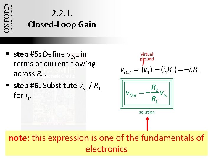
2. 2. 1. Closed-Loop Gain § step #5: Define v. Out in terms of current flowing across R 2. § step #6: Substitute vin / R 1 for i 1. note: this expression is one of the fundamentals of electronics Oxford University Publishing Microelectronic Circuits by Adel S. Sedra and Kenneth C. Smith (0195323033)

Figure 2. 6: Analysis 2. 2. 1. of the inverting configuration. The circled numbers indicate the order of the analysis steps. Closed-Loop Gain § question: how will we… § step #4: define v. Out in terms of current flowing across R 2 § step #5: substitute vin / R 1 for i 1. Oxford University Publishing Microelectronic Circuits by Adel S. Sedra and Kenneth C. Smith (0195323033) closed-loop gain G = -R 2/R 1

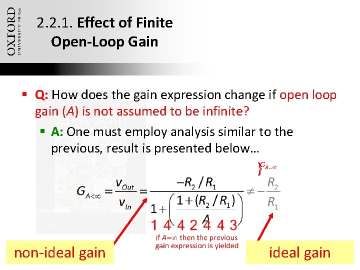
2. 2. 1. Effect of Finite Open-Loop Gain § Q: How does the gain expression change if open loop gain (A) is not assumed to be infinite? § A: One must employ analysis similar to the previous, result is presented below… non-ideal gain Oxford University Publishing Microelectronic Circuits by Adel S. Sedra and Kenneth C. Smith (0195323033) ideal gain

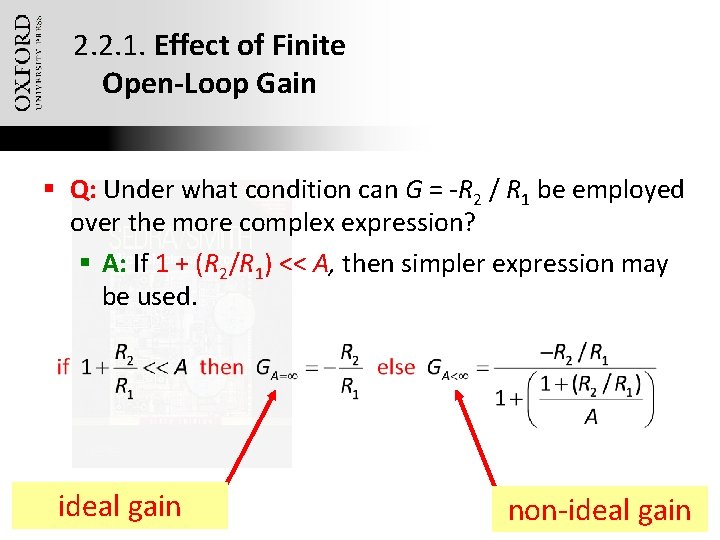
2. 2. 1. Effect of Finite Open-Loop Gain § Q: Under what condition can G = -R 2 / R 1 be employed over the more complex expression? § A: If 1 + (R 2/R 1) << A, then simpler expression may be used. ideal gain Oxford University Publishing Microelectronic Circuits by Adel S. Sedra and Kenneth C. Smith (0195323033) non-ideal gain

Example 2. 1: Simple Inverting Amplifier § Problem Statement: Consider an inverting configuration with R 1 = 1 k. Ohm and R 2 = 100 k. Ohm. § Q(a): Find the closed-loop gain (G) for the cases below. In each case, determine the percentage error in the magnitude of G relative to the ideal value. § cases are A = 103, 104, 105… § Q(b): What is the voltage v 1 that appears at the inverting input terminal when v. In = 0. 1 V. § Q(c): If the open loop gain (A) changes from 100 k to 50 k, what is percentage change in gain (G)? Oxford University Publishing Microelectronic Circuits by Adel S. Sedra and Kenneth C. Smith (0195323033)

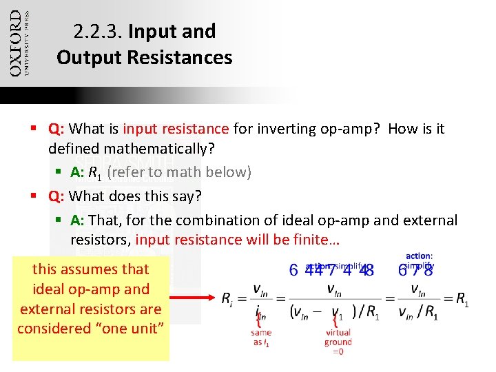
2. 2. 3. Input and Output Resistances § Q: What is input resistance for inverting op-amp? How is it defined mathematically? § A: R 1 (refer to math below) § Q: What does this say? § A: That, for the combination of ideal op-amp and external resistors, input resistance will be finite… this assumes that ideal op-amp and external resistors are considered “one unit” Oxford University Publishing Microelectronic Circuits by Adel S. Sedra and Kenneth C. Smith (0195323033)

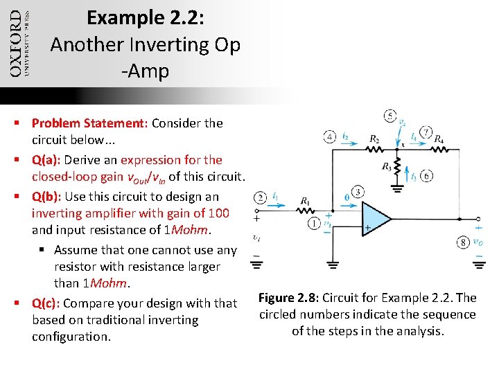
Example 2. 2: Another Inverting Op -Amp § Problem Statement: Consider the circuit below. . . § Q(a): Derive an expression for the closed-loop gain v. Out/v. In of this circuit. § Q(b): Use this circuit to design an inverting amplifier with gain of 100 and input resistance of 1 Mohm. § Assume that one cannot use any resistor with resistance larger than 1 Mohm. Figure 2. 8: Circuit for Example 2. 2. The § Q(c): Compare your design with that circled numbers indicate the sequence based on traditional inverting of the steps in the analysis. configuration. Oxford University Publishing Microelectronic Circuits by Adel S. Sedra and Kenneth C. Smith (0195323033)

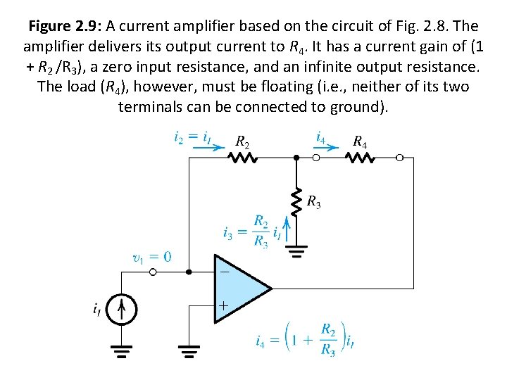
Example 2. 2: Figure 2. 9: A current amplifier based on the circuit of Fig. 2. 8. The amplifier delivers its output current to R 4. It has a current gain of (1 Another Inverting + R 2 /R 3), a zero input resistance, and an infinite output resistance. Op-Amp The load (R 4), however, must be floating (i. e. , neither of its two PART B: Use this circuit to design an inverting amplifier with gain of 100 and input resistance of 1 Mohm. Assume that one cannot use any resistor with resistance larger than 1 Mohm. terminals can be connected to ground). § The largest resistor on may choose is 1 Mohm § Q: Where does one begin (in choosing the resistor values)? Which resistor would you define to be 1 Mohm? § A: The input resistance (R 1) should be set as high as possible, therefore 1 Mohm § Q: What other resistor values should be defined? § A: R 2 = 1 Mohm, R 4 = 1 Mohm, R 3 = 10. 2 kohm Oxford University Publishing Microelectronic Circuits by Adel S. Sedra and Kenneth C. Smith (0195323033)

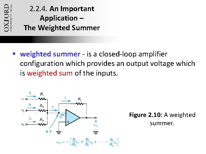
2. 2. 4. An Important Application – The Weighted Summer § weighted summer - is a closed-loop amplifier configuration which provides an output voltage which is weighted sum of the inputs. Figure 2. 10: A weighted summer. Oxford University Publishing Microelectronic Circuits by Adel S. Sedra and Kenneth C. Smith (0195323033)

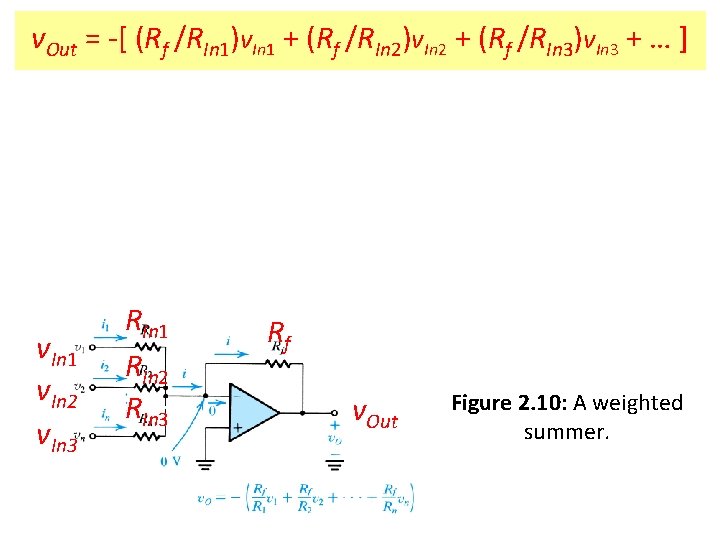
Important v. Out = 2. 2. 4. -[ (Rf. An /RIn 1 )v. In 1 + (Rf. /RIn 2)v. In 2 + (Rf. /RIn 3)v. In 3 + … ] Application – The Weighted Summer § weighted summer - is a closed-loop amplifier configuration which provides an output voltage which is weighted sum of the inputs. v. In 1 v. In 2 v. In 3 RIn 1 RIn 2 RIn 3 Rf Oxford University Publishing Microelectronic Circuits by Adel S. Sedra and Kenneth C. Smith (0195323033) v. Out Figure 2. 10: A weighted summer.

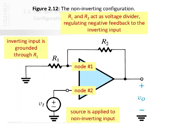
2. 3. The Non-Inverting Configuration § non-inverting op-amp configuration – is one which utilizes external resistances (like the previous) to effect voltage gain. However, the polarity / phase of the output is same as input. Oxford University Publishing Microelectronic Circuits by Adel S. Sedra and Kenneth C. Smith (0195323033)

Figure 2. 12: The non-inverting configuration. 2. 3. The Non-Inverting Configuration R 1 and R 2 act as voltage divider, regulating negative feedback to the inverting input is grounded through R 1 node #2 source is applied to non-inverting input Oxford University Publishing Microelectronic Circuits by Adel S. Sedra and Kenneth C. Smith (0195323033)

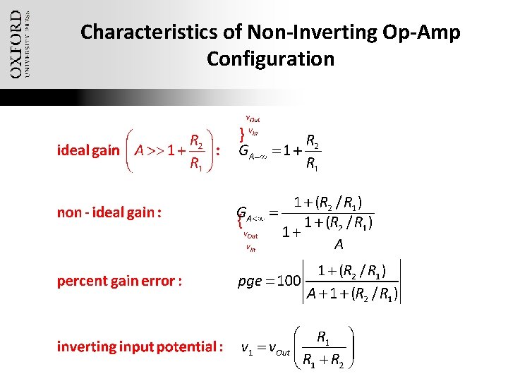
Characteristics of Non-Inverting Op-Amp Configuration Oxford University Publishing Microelectronic Circuits by Adel S. Sedra and Kenneth C. Smith (0195323033)

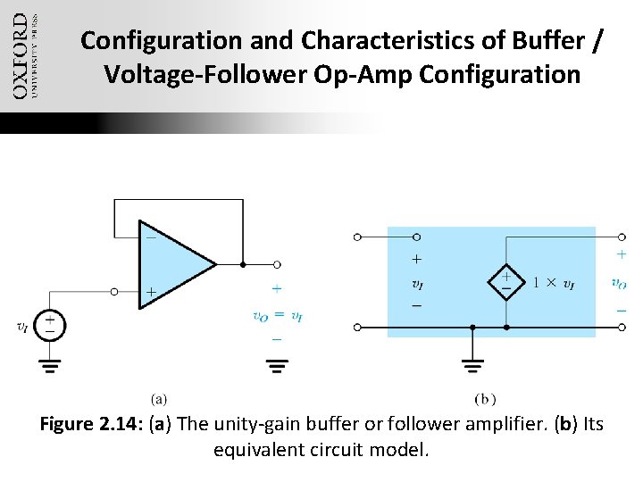
Configuration and Characteristics of Buffer / Voltage-Follower Op-Amp Configuration Figure 2. 14: (a) The unity-gain buffer or follower amplifier. (b) Its equivalent circuit model. Oxford University Publishing Microelectronic Circuits by Adel S. Sedra and Kenneth C. Smith (0195323033)

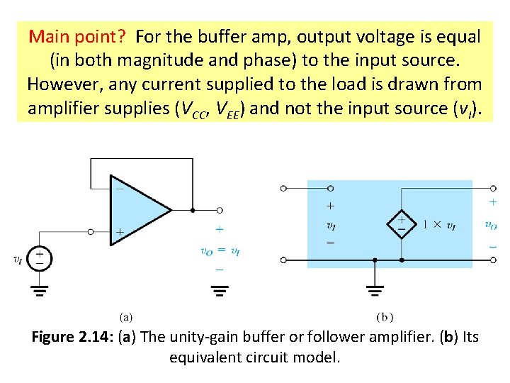
and Characteristics of Buffer / Main. Configuration point? For the buffer amp, output voltage is equal Voltage-Follower Op-Amp Configuration (in both magnitude and phase) to the input source. However, any current supplied to the load is drawn from amplifier supplies (VCC, VEE) and not the input source (v. I). Figure 2. 14: (a) The unity-gain buffer or follower amplifier. (b) Its equivalent circuit model. Oxford University Publishing Microelectronic Circuits by Adel S. Sedra and Kenneth C. Smith (0195323033)

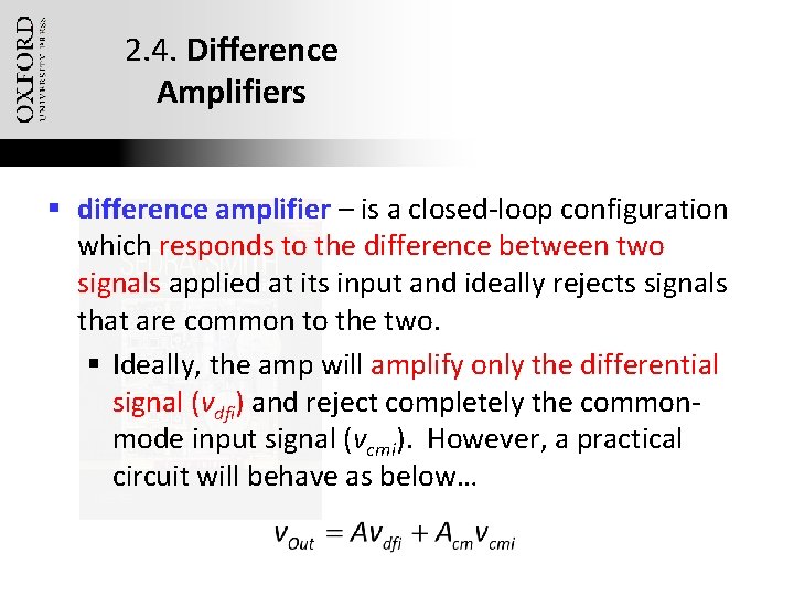
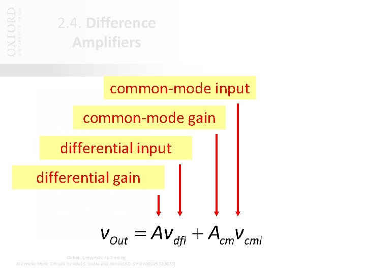
2. 4. Difference Amplifiers § difference amplifier – is a closed-loop configuration which responds to the difference between two signals applied at its input and ideally rejects signals that are common to the two. § Ideally, the amp will amplify only the differential signal (vdfi) and reject completely the commonmode input signal (vcmi). However, a practical circuit will behave as below… Oxford University Publishing Microelectronic Circuits by Adel S. Sedra and Kenneth C. Smith (0195323033)

2. 4. Difference Amplifiers common-mode input common-mode gain differential input differential gain Oxford University Publishing Microelectronic Circuits by Adel S. Sedra and Kenneth C. Smith (0195323033)

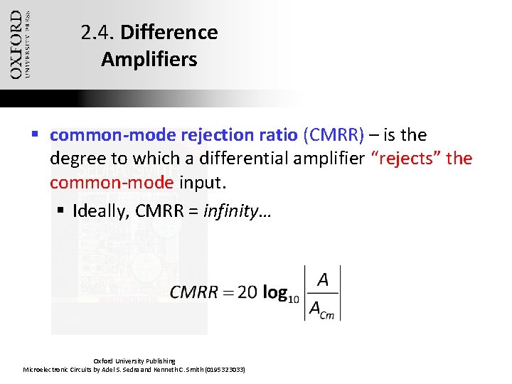
2. 4. Difference Amplifiers § common-mode rejection ratio (CMRR) – is the degree to which a differential amplifier “rejects” the common-mode input. § Ideally, CMRR = infinity… Oxford University Publishing Microelectronic Circuits by Adel S. Sedra and Kenneth C. Smith (0195323033)

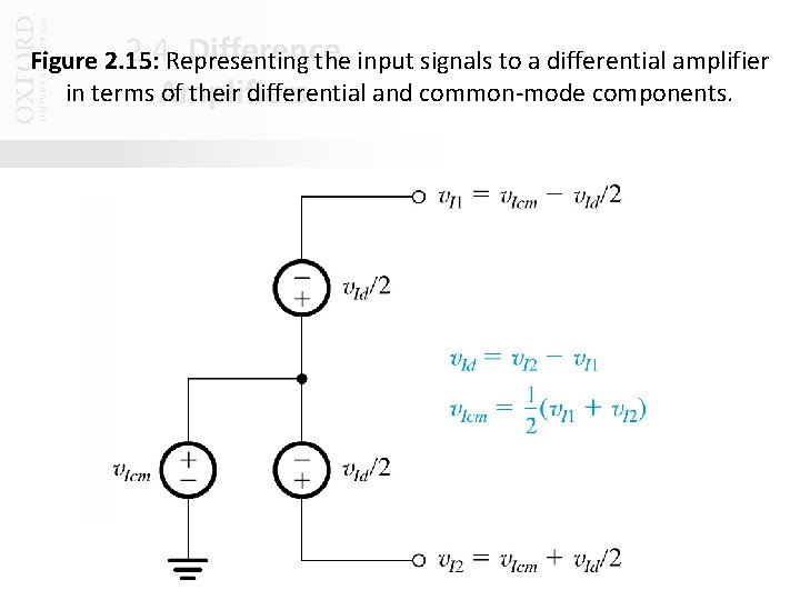
2. 4. Representing Difference Figure 2. 15: the input signals to a differential amplifier in terms Amplifiers of their differential and common-mode components. Oxford University Publishing Microelectronic Circuits by Adel S. Sedra and Kenneth C. Smith (0195323033)

2. 4. Difference Amplifiers § Q: The op amp itself is differential in nature, why cannot it be used by itself? § A: It has an infinite gain, and therefore cannot be used by itself. One must devise a closed-loop configuration which facilitates this operation. Oxford University Publishing Microelectronic Circuits by Adel S. Sedra and Kenneth C. Smith (0195323033)

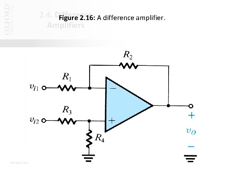
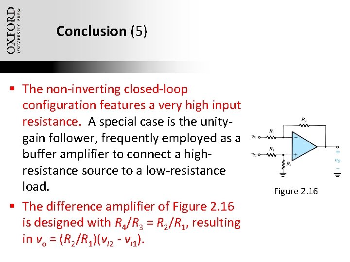
2. 4. Difference Figure 2. 16: A difference amplifier. Amplifiers Oxford University Publishing Microelectronic Circuits by Adel S. Sedra and Kenneth C. Smith (0195323033)

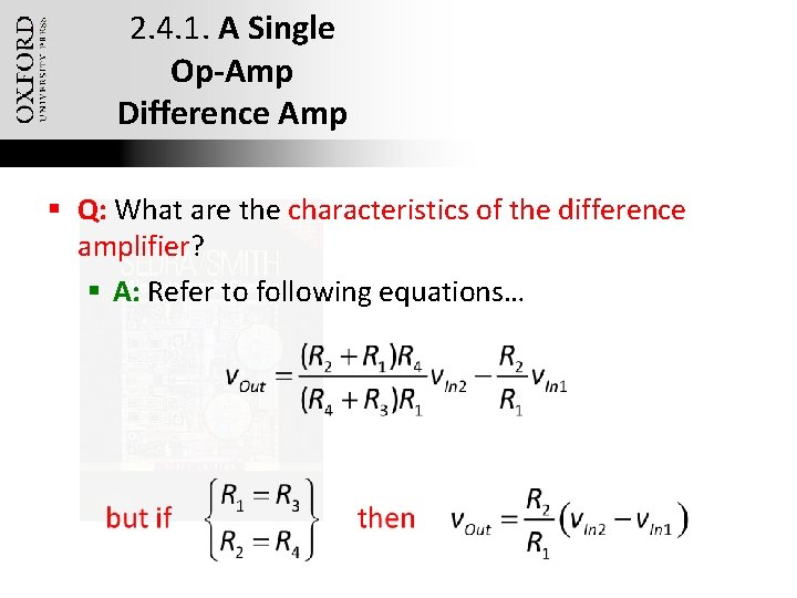
2. 4. 1. A Single Op-Amp Difference Amp § Q: What are the characteristics of the difference amplifier? § A: Refer to following equations… Oxford University Publishing Microelectronic Circuits by Adel S. Sedra and Kenneth C. Smith (0195323033)

A Shift in Notation § Before this point… § The parameter A is used to represent open-loop gain of an op amp. § The parameter G is used to represent ideal / non-ideal closed-loop gain of an op amp. § After this point… § The parameter A is used to represent ideal gain of an op amp in a given closed-loop configuration. § The parameter G is not used. Oxford University Publishing Microelectronic Circuits by Adel S. Sedra and Kenneth C. Smith (0195323033)

2. 4. 2. The Instrumentation Amplifier § Q: What is one problem associated with the difference amplifier? § A: Low input impedance. § Q: And, what does this mean practically? § A: That source impedance will have an effect on gain. § Q: What is the solution? § A: Placement of two buffers at the input terminals, amplifiers which transmit the voltage level but draw minimal current. Oxford University Publishing Microelectronic Circuits by Adel S. Sedra and Kenneth C. Smith (0195323033)

2. 4. 2. The Instrumentation Amplifier § Q: However, can one get “more” from these amps than simply impedance matching? § A: Yes, maybe additional voltage gain? ? ? Oxford University Publishing Microelectronic Circuits by Adel S. Sedra and Kenneth C. Smith (0195323033)

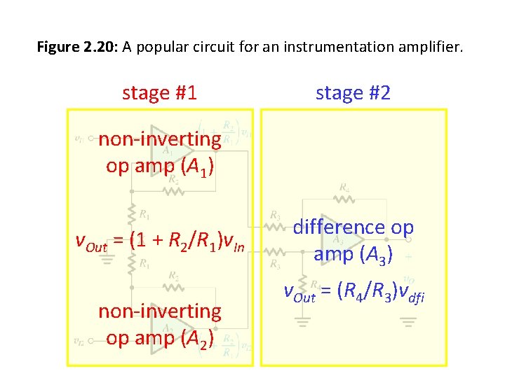
2. 4. 2. The Instrumentation Figure 2. 20: A popular circuit for an instrumentation amplifier. Amplifier stage #1 stage #2 § question: however, can we get “more” from these amps than simply non-inverting impedance matching? § answer: maybe(A additional voltage gain? ? ? opyes, amp 1) v. Out = (1 + R 2/R 1)v. In non-inverting op amp (A 2) Oxford University Publishing Microelectronic Circuits by Adel S. Sedra and Kenneth C. Smith (0195323033) difference op amp (A 3) v. Out = (R 4/R 3)vdfi

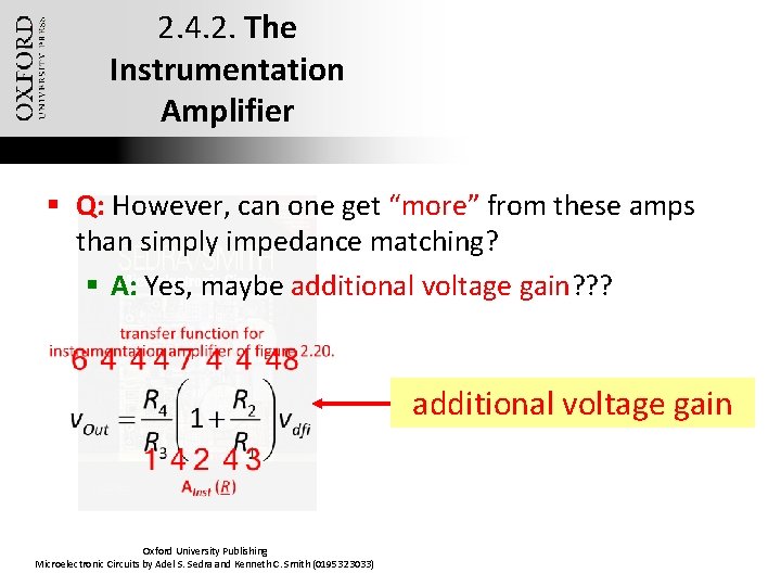
2. 4. 2. The Instrumentation Amplifier § Q: However, can one get “more” from these amps than simply impedance matching? § A: Yes, maybe additional voltage gain? ? ? additional voltage gain Oxford University Publishing Microelectronic Circuits by Adel S. Sedra and Kenneth C. Smith (0195323033)

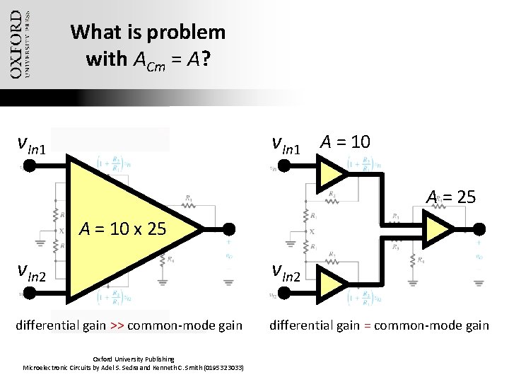
2. 4. 2. The Instrumentation Amplifier § advantages of instrumentation amp § very high input resistance § high differential gain § symmetric gain (assuming that A 1 and A 2 are matched) § disadvantages of instrumentation amp § ADi and ACm are equal in first stage – meaning that the common-mode and differential inputs are amplified with equal gain… Oxford University Publishing Microelectronic Circuits by Adel S. Sedra and Kenneth C. Smith (0195323033)

What is problem with ACm = A? v. In 1 A = 10 A = 25 A = 10 x 25 v. In 2 differential gain >> common-mode gain differential gain = common-mode gain Oxford University Publishing Microelectronic Circuits by Adel S. Sedra and Kenneth C. Smith (0195323033)

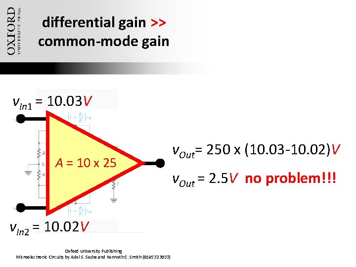
differential gain >> common-mode gain v. In 1 = 10. 03 V A = 10 x 25 v. In 2 = 10. 02 V Oxford University Publishing Microelectronic Circuits by Adel S. Sedra and Kenneth C. Smith (0195323033) v. Out= 250 x (10. 03 -10. 02)V v. Out = 2. 5 V no problem!!!

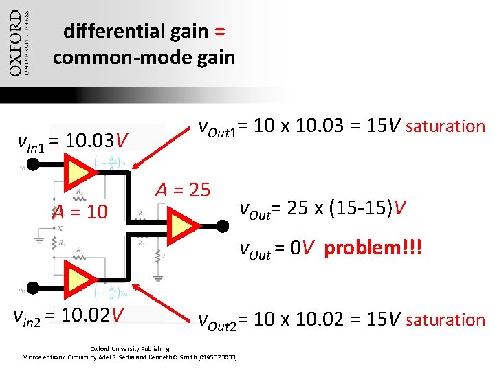
differential gain = common-mode gain v. In 1 = 10. 03 V A = 10 v. Out 1= 10 x 10. 03 = 15 V saturation A = 25 v. Out= 25 x (15 -15)V v. Out = 0 V problem!!! v. In 2 = 10. 02 V v. Out 2= 10 x 10. 02 = 15 V saturation Oxford University Publishing Microelectronic Circuits by Adel S. Sedra and Kenneth C. Smith (0195323033)

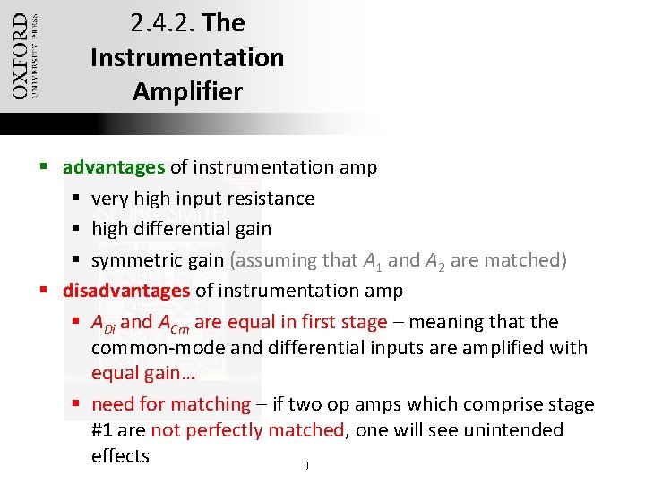
2. 4. 2. The Instrumentation Amplifier § advantages of instrumentation amp § very high input resistance § high differential gain § symmetric gain (assuming that A 1 and A 2 are matched) § disadvantages of instrumentation amp § ADi and ACm are equal in first stage – meaning that the common-mode and differential inputs are amplified with equal gain… § need for matching – if two op amps which comprise stage #1 are not perfectly matched, one will see unintended Oxford University Publishing effects Microelectronic Circuits by Adel S. Sedra and Kenneth C. Smith (0195323033)

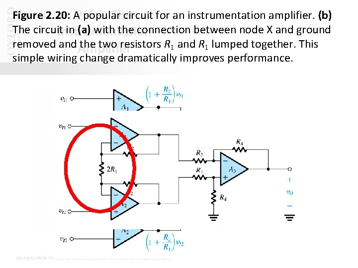
2. 4. 2. The Instrumentation Amplifier § Q: How can one fix this (alleviate these disadvantages)? § A: Disconnect the two resistors (R 1) connected to node X from ground, making the configuration “floating” in nature… § A: Refer to following slide… Oxford University Publishing Microelectronic Circuits by Adel S. Sedra and Kenneth C. Smith (0195323033)

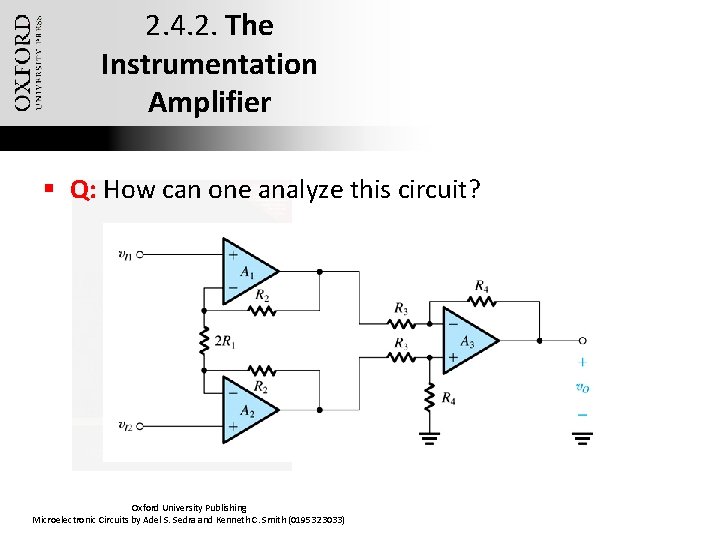
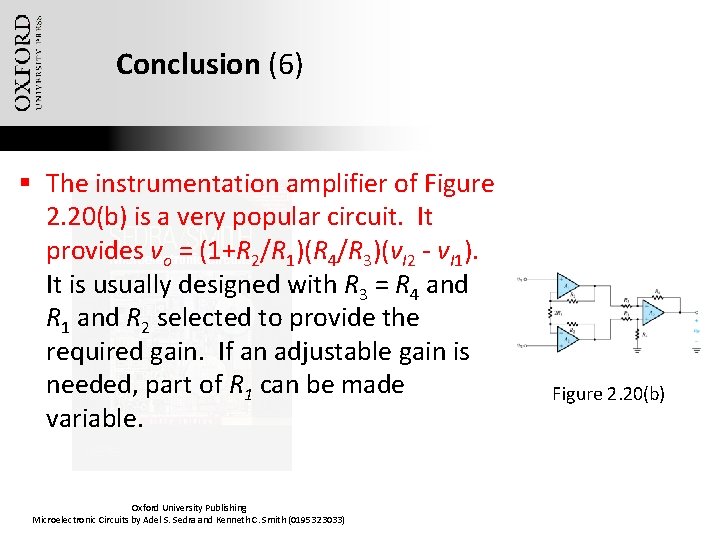
Figure 2. 20: A 2. 4. 2. popular circuit for an instrumentation amplifier. (b) The circuit in (a) with the connection between node X and ground Instrumentation removed and Amplifier the two resistors R 1 and R 1 lumped together. This simple wiring change dramatically improves performance. Oxford University Publishing Microelectronic Circuits by Adel S. Sedra and Kenneth C. Smith (0195323033)

2. 4. 2. The Instrumentation Amplifier § Q: How can one analyze this circuit? Oxford University Publishing Microelectronic Circuits by Adel S. Sedra and Kenneth C. Smith (0195323033)

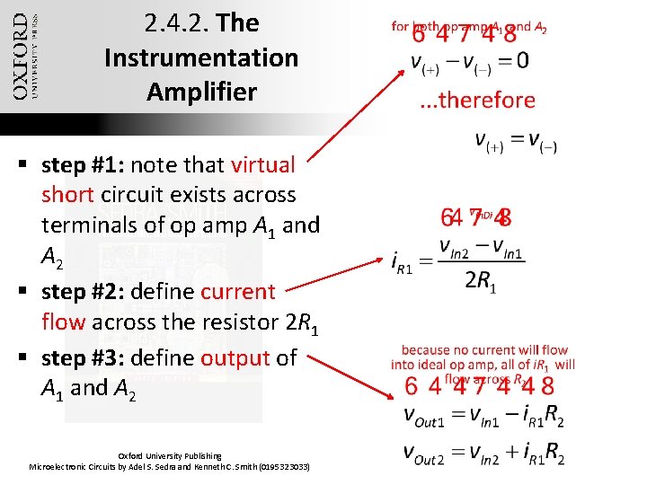
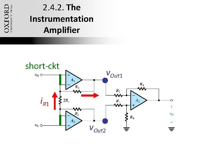
2. 4. 2. The Instrumentation Amplifier § step #1: note that virtual short circuit exists across terminals of op amp A 1 and A 2 § step #2: define current flow across the resistor 2 R 1 § step #3: define output of A 1 and A 2 Oxford University Publishing Microelectronic Circuits by Adel S. Sedra and Kenneth C. Smith (0195323033)

2. 4. 2. The Instrumentation Amplifier short-ckt v. Out 1 i. R 1 v. Out 2 Oxford University Publishing Microelectronic Circuits by Adel S. Sedra and Kenneth C. Smith (0195323033)

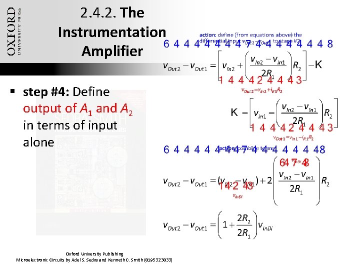
2. 4. 2. The Instrumentation Amplifier § step #4: Define output of A 1 and A 2 in terms of input alone Oxford University Publishing Microelectronic Circuits by Adel S. Sedra and Kenneth C. Smith (0195323033)

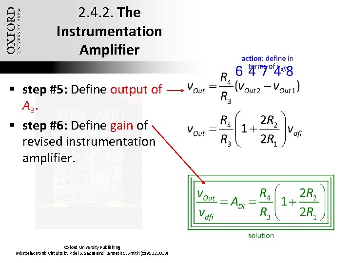
2. 4. 2. The Instrumentation Amplifier § step #5: Define output of A 3. § step #6: Define gain of revised instrumentation amplifier. Oxford University Publishing Microelectronic Circuits by Adel S. Sedra and Kenneth C. Smith (0195323033)

2. 5. Integrators and Differentiators § integrator / differentiator amplifier – is one which outputs an integral or derivative of the input signal. Oxford University Publishing Microelectronic Circuits by Adel S. Sedra and Kenneth C. Smith (0195323033)

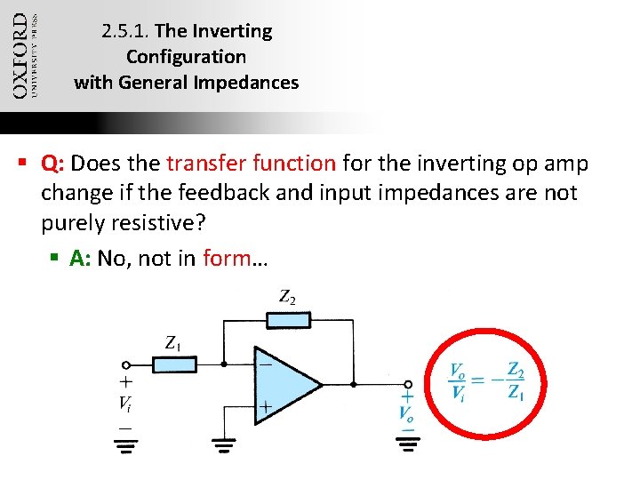
2. 5. 1. The Inverting Configuration with General Impedances § Q: Does the transfer function for the inverting op amp change if the feedback and input impedances are not purely resistive? § A: No, not in form… Oxford University Publishing Microelectronic Circuits by Adel S. Sedra and Kenneth C. Smith (0195323033)

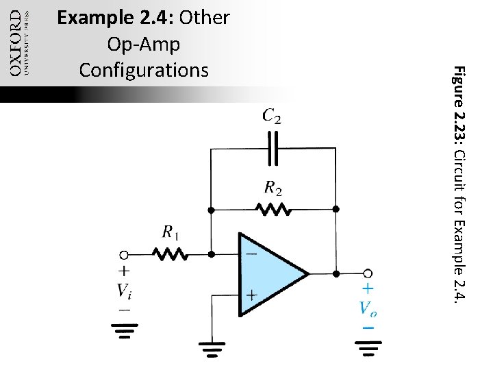
Example 2. 4: Other Op-Amp Configurations § Consider the circuit on next slide page. § Q(a): Derive an expression for the transfer function v. Out / v. In. § Q(b): Show that the transfer function is of a low-pass STC circuit. § Q(c): By expressing the transfer function in standard form of Table 1. 2, find the dc-gain and 3 d. B frequency. Oxford University Publishing Microelectronic Circuits by Adel S. Sedra and Kenneth C. Smith (0195323033)

Oxford University Publishing Microelectronic Circuits by Adel S. Sedra and Kenneth C. Smith (0195323033) Figure 2. 23: Circuit for Example 2. 4: Other Op-Amp Configurations

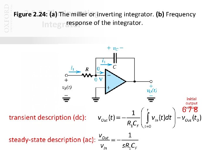
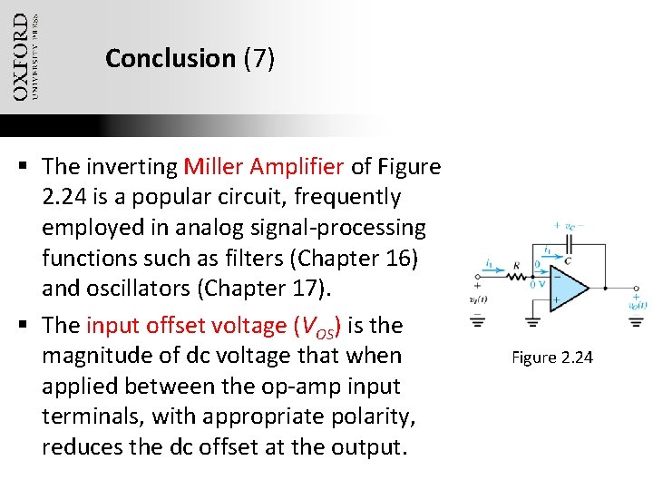
2. 5. 2. The Inverting Integrator § Q: How can inverting op-amp be adapted to perform integration? § A: Utilization of capacitor as feedback impedance. Oxford University Publishing Microelectronic Circuits by Adel S. Sedra and Kenneth C. Smith (0195323033)

2. 5. 2. Inverting Figure 2. 24: The (a) The miller or inverting integrator. (b) Frequency response of the integrator. Integrator Oxford University Publishing Microelectronic Circuits by Adel S. Sedra and Kenneth C. Smith (0195323033)

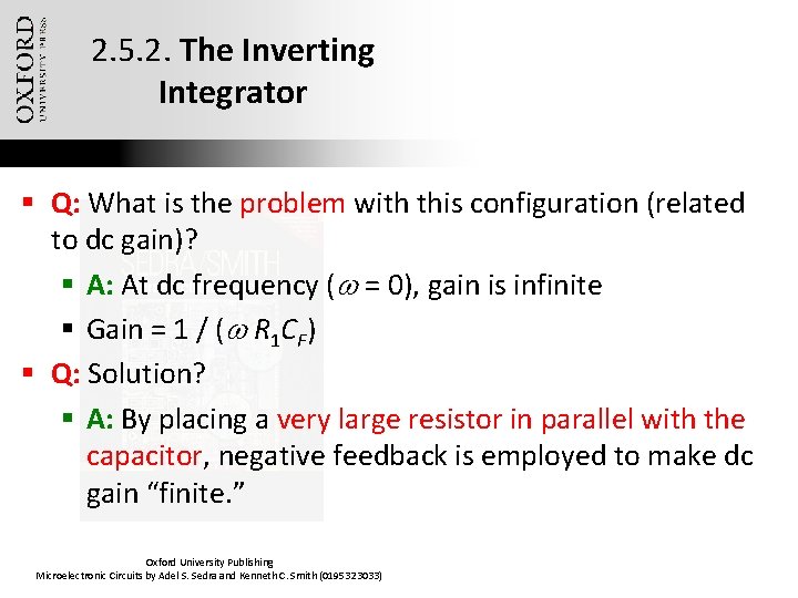
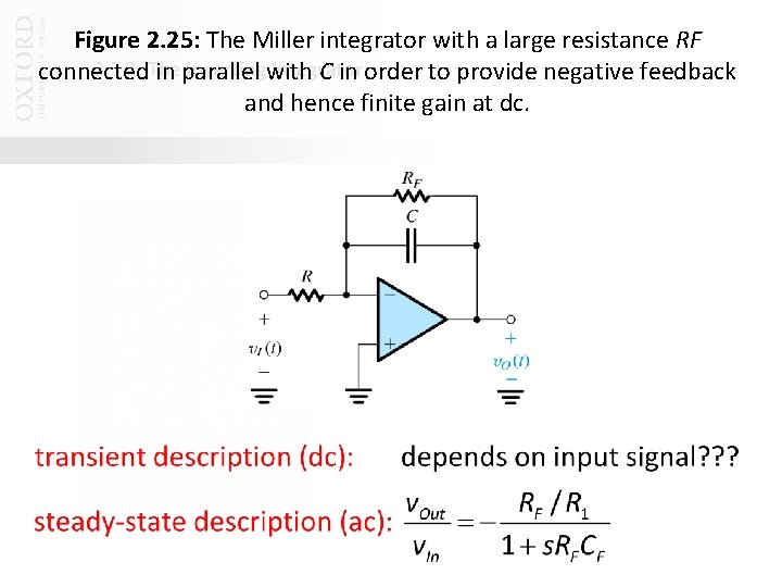
2. 5. 2. The Inverting Integrator § Q: What is the problem with this configuration (related to dc gain)? § A: At dc frequency (w = 0), gain is infinite § Gain = 1 / (w. R 1 CF) § Q: Solution? § A: By placing a very large resistor in parallel with the capacitor, negative feedback is employed to make dc gain “finite. ” Oxford University Publishing Microelectronic Circuits by Adel S. Sedra and Kenneth C. Smith (0195323033)

Figure 2. 25: The Miller integrator with a large resistance RF 2. 5. 2. The Invertingwith Integrator connected in parallel C in order to provide negative feedback and hence finite gain at dc. Oxford University Publishing Microelectronic Circuits by Adel S. Sedra and Kenneth C. Smith (0195323033)

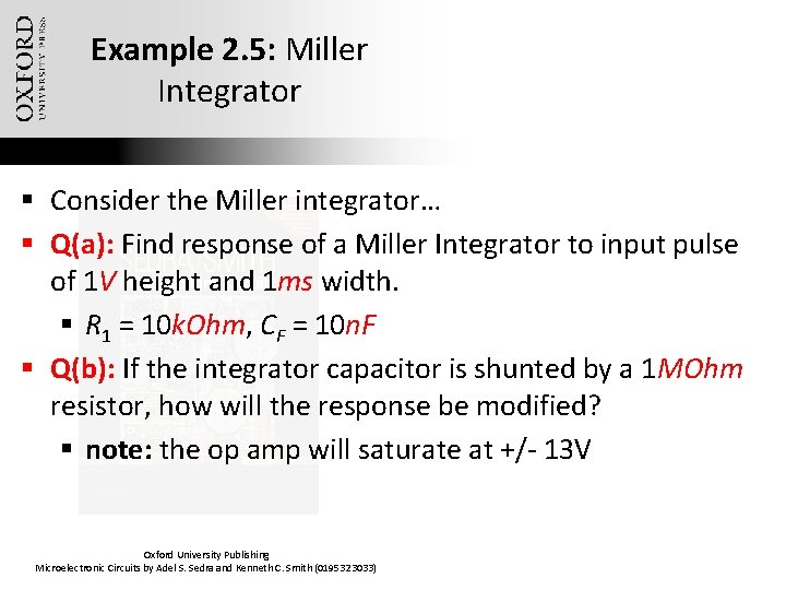
Example 2. 5: Miller Integrator § Consider the Miller integrator… § Q(a): Find response of a Miller Integrator to input pulse of 1 V height and 1 ms width. § R 1 = 10 k. Ohm, CF = 10 n. F § Q(b): If the integrator capacitor is shunted by a 1 MOhm resistor, how will the response be modified? § note: the op amp will saturate at +/- 13 V Oxford University Publishing Microelectronic Circuits by Adel S. Sedra and Kenneth C. Smith (0195323033)

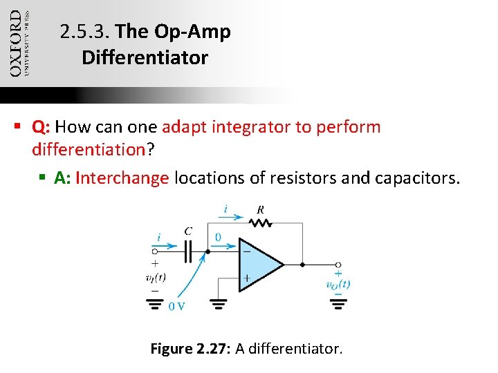
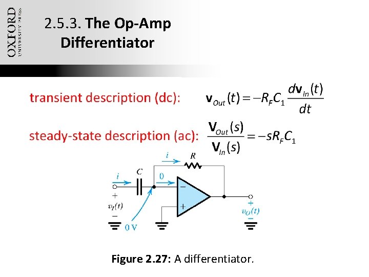
2. 5. 3. The Op-Amp Differentiator § Q: How can one adapt integrator to perform differentiation? § A: Interchange locations of resistors and capacitors. Figure 2. 27: A differentiator. Oxford University Publishing Microelectronic Circuits by Adel S. Sedra and Kenneth C. Smith (0195323033)

2. 5. 3. The Op-Amp Differentiator Figure 2. 27: A differentiator. Oxford University Publishing Microelectronic Circuits by Adel S. Sedra and Kenneth C. Smith (0195323033)

2. 5. 3. The Op-Amp Differentiator filtering characteristic is high pass filter magnitude of transfer function is |VOut / VIn| = w. RFC 1 phase of transfer function is f = -90 O differentiator time-constant is frequency at which unity gain occurs and defined as w = 1 / RFC 1 § Q: What is the problem with differentiator? § A: Differentiator acts as noise amplifier, exhibiting large changes in output from small (but fast) changes in input. As such, it is rarely used in practice. § § Oxford University Publishing Microelectronic Circuits by Adel S. Sedra and Kenneth C. Smith (0195323033)

2. 6. DC Imperfections § Q: What will be discussed moving on? § A: When can one NOT consider an op amp to be ideal, and what effect will that have on operation? Oxford University Publishing Microelectronic Circuits by Adel S. Sedra and Kenneth C. Smith (0195323033)

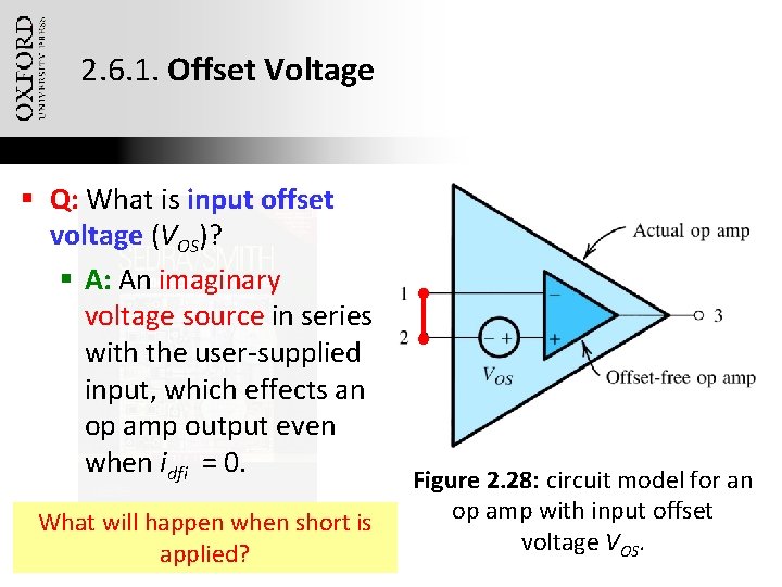
2. 6. 1. Offset Voltage § Q: What is input offset voltage (VOS)? § A: An imaginary voltage source in series with the user-supplied input, which effects an op amp output even when idfi = 0. What will happen when short is Oxford University Publishing applied? Microelectronic Circuits by Adel S. Sedra and Kenneth C. Smith (0195323033) Figure 2. 28: circuit model for an op amp with input offset voltage VOS.

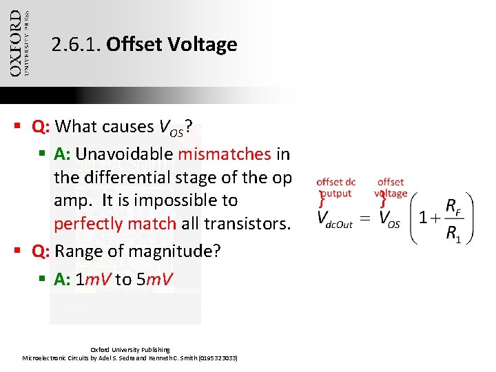
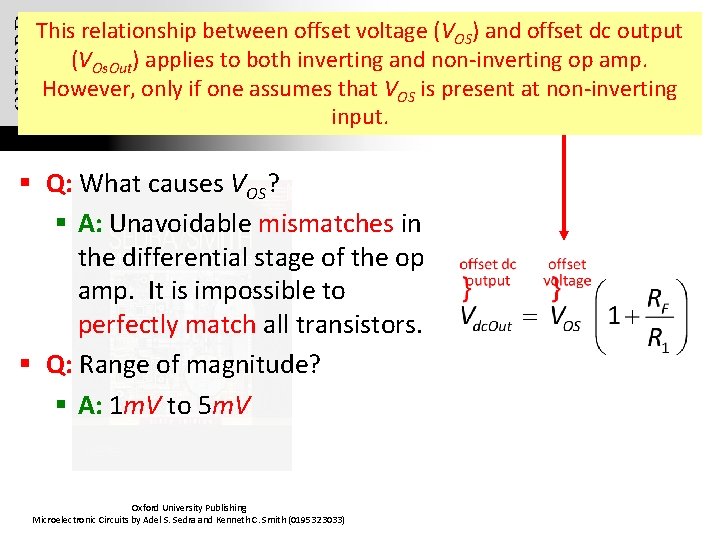
2. 6. 1. Offset Voltage § Q: What causes VOS? § A: Unavoidable mismatches in the differential stage of the op amp. It is impossible to perfectly match all transistors. § Q: Range of magnitude? § A: 1 m. V to 5 m. V Oxford University Publishing Microelectronic Circuits by Adel S. Sedra and Kenneth C. Smith (0195323033)

This relationship between offset voltage (VOS) and offset dc output (V to Voltage both inverting and non-inverting op amp. Os. Out) applies 2. 6. 1. Offset However, only if one assumes that VOS is present at non-inverting input. § Q: What causes VOS? § A: Unavoidable mismatches in the differential stage of the op amp. It is impossible to perfectly match all transistors. § Q: Range of magnitude? § A: 1 m. V to 5 m. V Oxford University Publishing Microelectronic Circuits by Adel S. Sedra and Kenneth C. Smith (0195323033)

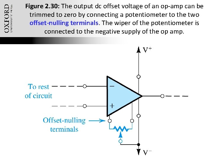
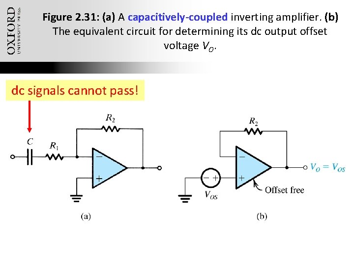
2. 6. 1. Offset Voltage § Q: How can this offset be reduced? § A: offset nulling terminals – A variable resistor (if properly set) may be used to reduce the asymmetry present and, in turn, reduce offset. § A: capacitive coupling – A series capacitor placed between the source and op amp may be used to reduce offset, although it will also filter out dc signals. Oxford University Publishing Microelectronic Circuits by Adel S. Sedra and Kenneth C. Smith (0195323033)

Figure 2. 30: The output dc offset voltage of an op-amp can be trimmed to zero by connecting a potentiometer to the two offset-nulling terminals. The wiper of the potentiometer is connected to the negative supply of the op amp. Oxford University Publishing Microelectronic Circuits by Adel S. Sedra and Kenneth C. Smith (0195323033)

Figure 2. 31: (a) A capacitively-coupled inverting amplifier. (b) The equivalent circuit for determining its dc output offset voltage VO. dc signals cannot pass! Oxford University Publishing Microelectronic Circuits by Adel S. Sedra and Kenneth C. Smith (0195323033)

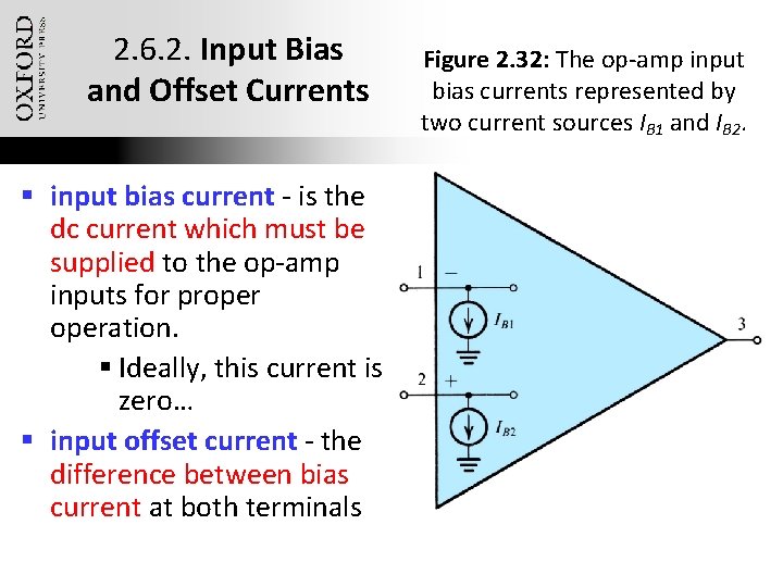
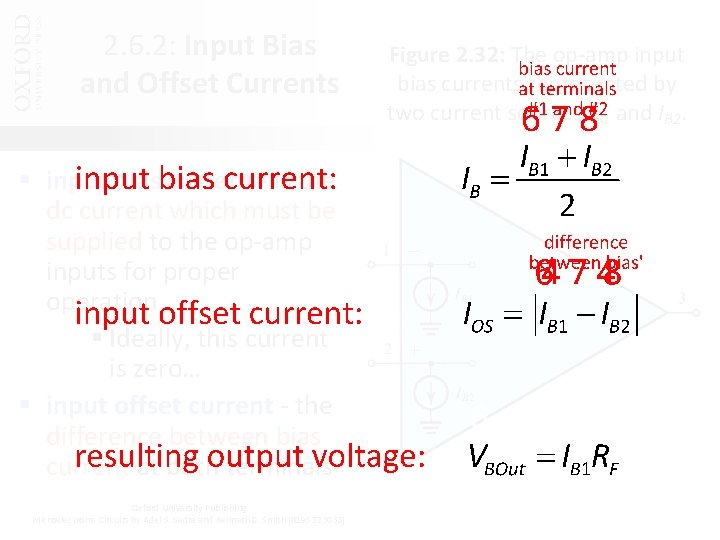
2. 6. 2. Input Bias and Offset Currents § input bias current - is the dc current which must be supplied to the op-amp inputs for properation. § Ideally, this current is zero… § input offset current - the difference between bias current at both terminals Oxford University Publishing Microelectronic Circuits by Adel S. Sedra and Kenneth C. Smith (0195323033) Figure 2. 32: The op-amp input bias currents represented by two current sources IB 1 and IB 2.

2. 6. 2: Input Bias and Offset Currents § input bias current - is the dc current which must be supplied to the op-amp inputs for properation. § Ideally, this current is zero… § input offset current - the difference between bias current at both terminals Oxford University Publishing Microelectronic Circuits by Adel S. Sedra and Kenneth C. Smith (0195323033) Figure 2. 32: The op-amp input bias currents represented by two current sources IB 1 and IB 2.

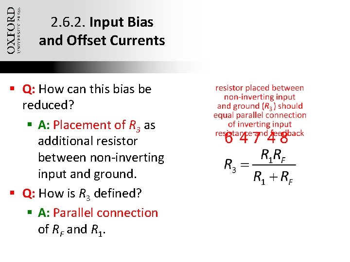
2. 6. 2. Input Bias and Offset Currents § Q: How can this bias be reduced? § A: Placement of R 3 as additional resistor between non-inverting input and ground. § Q: How is R 3 defined? § A: Parallel connection of RF and R 1. Oxford University Publishing Microelectronic Circuits by Adel S. Sedra and Kenneth C. Smith (0195323033)

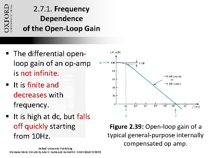
2. 7. 1. Frequency Dependence of the Open-Loop Gain § The differential openloop gain of an op-amp is not infinite. § It is finite and decreases with frequency. § It is high at dc, but falls off quickly starting from 10 Hz. Oxford University Publishing Microelectronic Circuits by Adel S. Sedra and Kenneth C. Smith (0195323033) Figure 2. 39: Open-loop gain of a typical general-purpose internally compensated op amp.

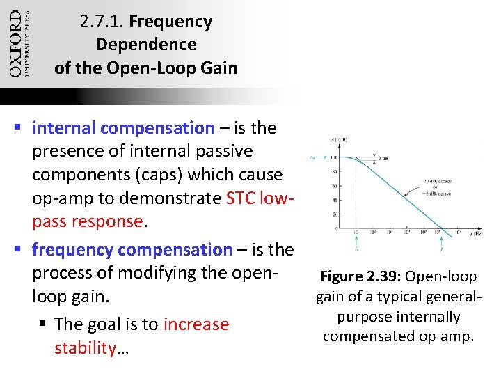
2. 7. 1. Frequency Dependence of the Open-Loop Gain § internal compensation – is the presence of internal passive components (caps) which cause op-amp to demonstrate STC lowpass response. § frequency compensation – is the process of modifying the openloop gain. § The goal is to increase stability… Oxford University Publishing Microelectronic Circuits by Adel S. Sedra and Kenneth C. Smith (0195323033) Figure 2. 39: Open-loop gain of a typical generalpurpose internally compensated op amp.

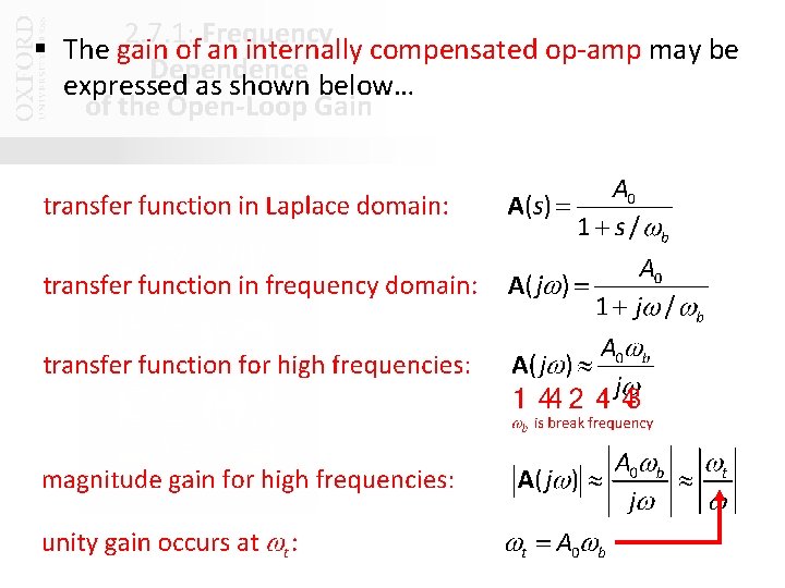
2. 7. 1: Frequency § The gain of an internally compensated op-amp may be Dependence expressed as shown below… of the Open-Loop Gain Oxford University Publishing Microelectronic Circuits by Adel S. Sedra and Kenneth C. Smith (0195323033)

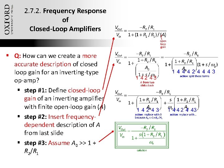
2. 7. 2. Frequency Response of Closed-Loop Amplifiers § Q: How can we create a more accurate description of closed loop gain for an inverting-type op-amp? § step #1: Define closed-loop gain of an inverting amplifier with finite open-loop gain (A) § step #2: Insert frequencydependent description of A from last slide § step #3: Assume A 0 >> 1 + R 2/R 1 Oxford University Publishing Microelectronic Circuits by Adel S. Sedra and Kenneth C. Smith (0195323033)

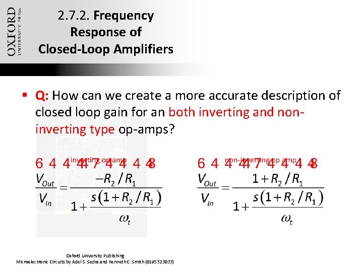
2. 7. 2. Frequency Response of Closed-Loop Amplifiers § Q: How can we create a more accurate description of closed loop gain for an both inverting and noninverting type op-amps? Oxford University Publishing Microelectronic Circuits by Adel S. Sedra and Kenneth C. Smith (0195323033)

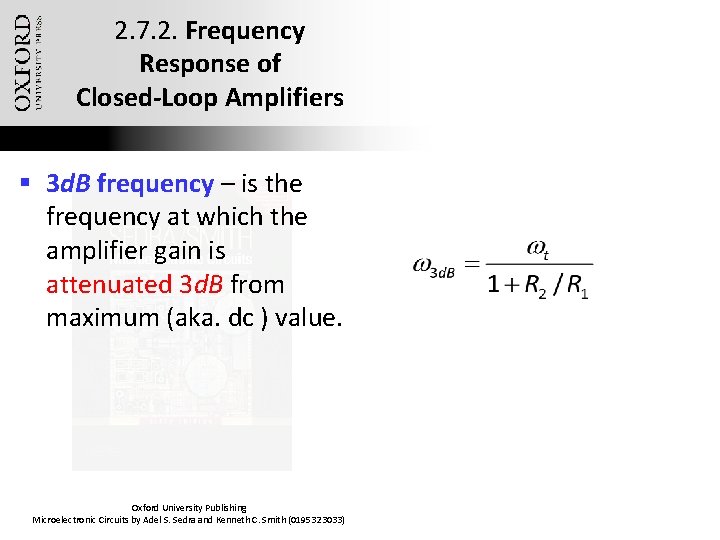
2. 7. 2. Frequency Response of Closed-Loop Amplifiers § 3 d. B frequency – is the frequency at which the amplifier gain is attenuated 3 d. B from maximum (aka. dc ) value. Oxford University Publishing Microelectronic Circuits by Adel S. Sedra and Kenneth C. Smith (0195323033)

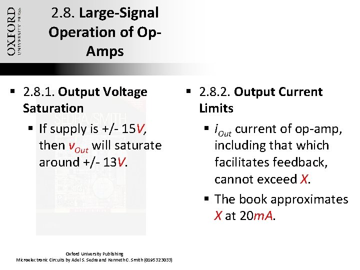
2. 8. Large-Signal Operation of Op. Amps § 2. 8. 1. Output Voltage Saturation § If supply is +/- 15 V, then v. Out will saturate around +/- 13 V. Oxford University Publishing Microelectronic Circuits by Adel S. Sedra and Kenneth C. Smith (0195323033) § 2. 8. 2. Output Current Limits § i. Out current of op-amp, including that which facilitates feedback, cannot exceed X. § The book approximates X at 20 m. A.

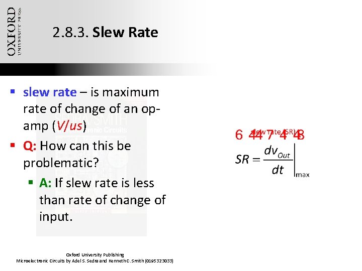
2. 8. 3. Slew Rate § slew rate – is maximum rate of change of an opamp (V/us) § Q: How can this be problematic? § A: If slew rate is less than rate of change of input. Oxford University Publishing Microelectronic Circuits by Adel S. Sedra and Kenneth C. Smith (0195323033)

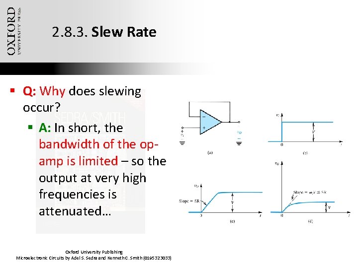
2. 8. 3. Slew Rate § Q: Why does slewing occur? § A: In short, the bandwidth of the opamp is limited – so the output at very high frequencies is attenuated… Oxford University Publishing Microelectronic Circuits by Adel S. Sedra and Kenneth C. Smith (0195323033)

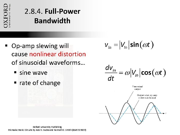
2. 8. 4. Full-Power Bandwidth § Op-amp slewing will cause nonlinear distortion of sinusoidal waveforms… § sine wave § rate of change Oxford University Publishing Microelectronic Circuits by Adel S. Sedra and Kenneth C. Smith (0195323033)

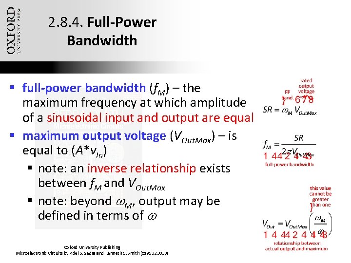
2. 8. 4. Full-Power Bandwidth § full-power bandwidth (f. M) – the maximum frequency at which amplitude of a sinusoidal input and output are equal § maximum output voltage (VOut. Max) – is equal to (A*v. In) § note: an inverse relationship exists between f. M and VOut. Max § note: beyond w. M, output may be defined in terms of w Oxford University Publishing Microelectronic Circuits by Adel S. Sedra and Kenneth C. Smith (0195323033)

Conclusion § The IC op-amp is a versatile circuit building block. It is easy to apply, and the performance of op-amp circuits closely matches theoretical predictions. § The op-amp terminals are the inverting terminal (1), the non-inverting input terminal (2), the output terminal (3), the positive-supply terminal (4) to be connected to the positive power supply (VCC), and the negative-supply terminal (5) to be connected to the negative supply (-VEE). Oxford University Publishing Microelectronic Circuits by Adel S. Sedra and Kenneth C. Smith (0195323033)

Conclusion (2) § The ideal op-amp responds only to the difference input signal, that is (v 2 - v 1). It yields an output between terminals 3 and ground of A(v 2 - v 1). The open-loop gain (A) is assumed to be infinite. The input resistance (Rin) is infinite. The output resistance (Rout) is assumed to be zero. § Negative feedback is applied to an op-amp by connecting a passive component between its output terminal and its inverting (aka. negative) input terminal. Oxford University Publishing Microelectronic Circuits by Adel S. Sedra and Kenneth C. Smith (0195323033)

Conclusion (3) § Negative feedback causes the voltage between the two input terminals to become very small, and ideally zero. Correspondingly, a virtual short is said to exist between the two input terminals. If the positive input terminal is connected to ground, a virtual ground appears on the negative terminal. Oxford University Publishing Microelectronic Circuits by Adel S. Sedra and Kenneth C. Smith (0195323033)

Conclusion (4) § The two most important assumptions in the analysis of op-amp circuits, assuming negative feedback exists, are: § the two input terminals of the op-amp are at the same voltage potential. § zero current flows into the op-amp input terminals. § With negative feedback applied and the loop closed, the gain is almost entirely determined by external components: Vo/Vi = -R 2/R 1 or 1+R 2/R 1. Oxford University Publishing Microelectronic Circuits by Adel S. Sedra and Kenneth C. Smith (0195323033)

Conclusion (5) § The non-inverting closed-loop configuration features a very high input resistance. A special case is the unitygain follower, frequently employed as a buffer amplifier to connect a highresistance source to a low-resistance load. § The difference amplifier of Figure 2. 16 is designed with R 4/R 3 = R 2/R 1, resulting in vo = (R 2/R 1)(v. I 2 - v. I 1). Oxford University Publishing Microelectronic Circuits by Adel S. Sedra and Kenneth C. Smith (0195323033) Figure 2. 16

Conclusion (6) § The instrumentation amplifier of Figure 2. 20(b) is a very popular circuit. It provides vo = (1+R 2/R 1)(R 4/R 3)(v. I 2 - v. I 1). It is usually designed with R 3 = R 4 and R 1 and R 2 selected to provide the required gain. If an adjustable gain is needed, part of R 1 can be made variable. Oxford University Publishing Microelectronic Circuits by Adel S. Sedra and Kenneth C. Smith (0195323033) Figure 2. 20(b)

Conclusion (7) § The inverting Miller Amplifier of Figure 2. 24 is a popular circuit, frequently employed in analog signal-processing functions such as filters (Chapter 16) and oscillators (Chapter 17). § The input offset voltage (VOS) is the magnitude of dc voltage that when applied between the op-amp input terminals, with appropriate polarity, reduces the dc offset at the output. Oxford University Publishing Microelectronic Circuits by Adel S. Sedra and Kenneth C. Smith (0195323033) Figure 2. 24