CCD Technology NEON School 2013 Dr Simon Tulloch




- Slides: 54

CCD Technology NEON School 2013 Dr. Simon Tulloch University of Sheffield Photoelectric Effect Charge collection Basic CCD structure Thinning Charge Transfer Blooming Dark Current Image defects Cosmic rays Fringing Anti-reflection coats Quantum Efficiency Camera Construction June 24 th 2013

1. 4. The CCD

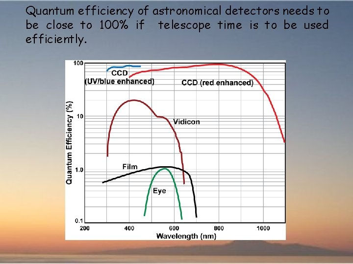
Quantum efficiency of astronomical detectors needs to be close to 100% if telescope time is to be used efficiently.

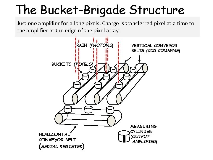
The Bucket-Brigade Structure Just one amplifier for all the pixels. Charge is transferred pixel at a time to the amplifier at the edge of the pixel array. RAIN (PHOTONS) VERTICAL CONVEYOR BELTS (CCD COLUMNS) BUCKETS (PIXELS) HORIZONTAL CONVEYOR BELT (SERIAL REGISTER) MEASURING CYLINDER (OUTPUT AMPLIFIER)

Read out proceeds until all pixel buckets have been measured. `

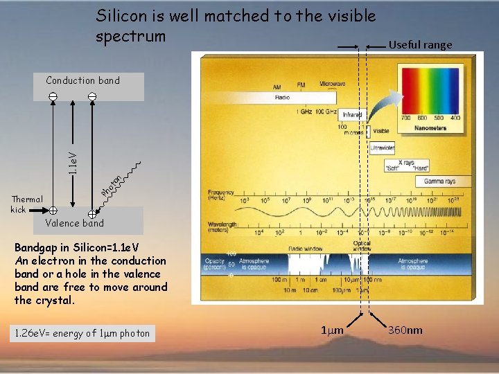
Silicon is well matched to the visible spectrum Useful range Thermal kick Ph ot on 1. 1 e. V Conduction band Valence band Bandgap in Silicon=1. 1 e. V An electron in the conduction band or a hole in the valence band are free to move around the crystal. 1. 26 e. V= energy of 1 mm photon 1 mm 360 nm

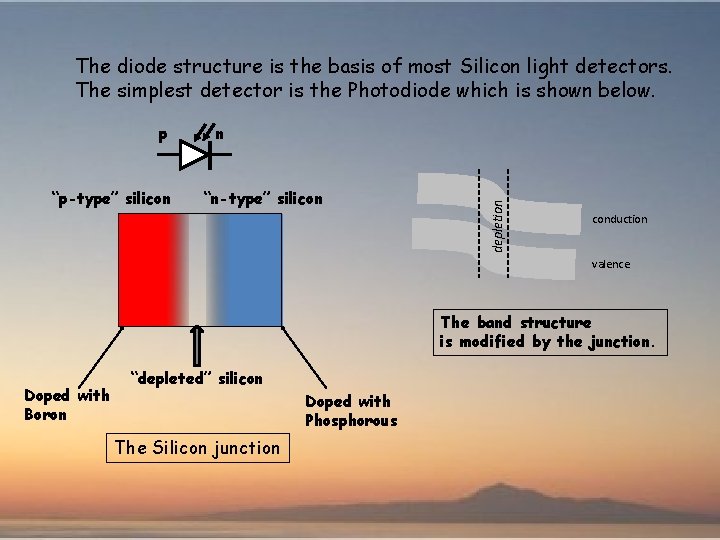
The diode structure is the basis of most Silicon light detectors. The simplest detector is the Photodiode which is shown below. “p-type” silicon n “n-type” silicon depletion p conduction valence The band structure is modified by the junction. Doped with Boron “depleted” silicon Doped with Phosphorous The Silicon junction

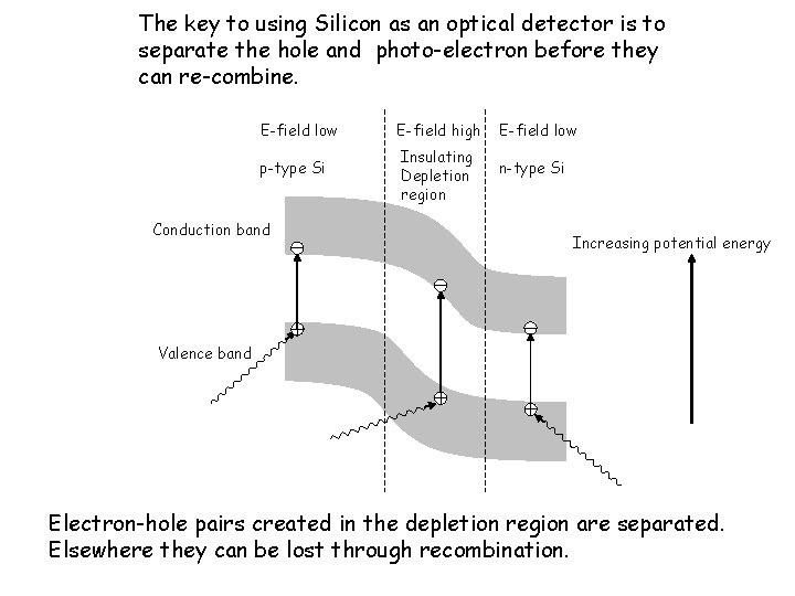
The key to using Silicon as an optical detector is to separate the hole and photo-electron before they can re-combine. E-field low p-type Si Conduction band E-field high Insulating Depletion region E-field low n-type Si Increasing potential energy Valence band Electron-hole pairs created in the depletion region are separated. Elsewhere they can be lost through recombination.

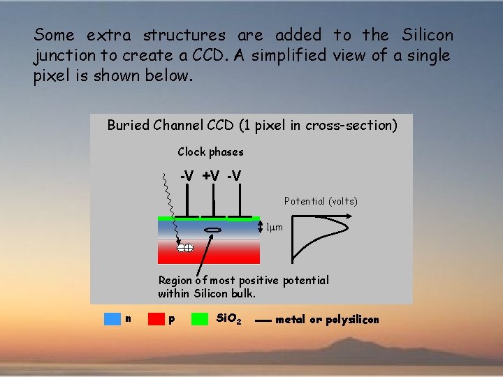
Some extra structures are added to the Silicon junction to create a CCD. A simplified view of a single pixel is shown below. Buried Channel CCD (1 pixel in cross-section) Clock phases -V +V -V Potential (volts) 1 mm Region of most positive potential within Silicon bulk. n p Si. O 2 metal or polysilicon

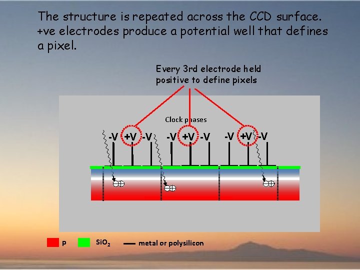
The structure is repeated across the CCD surface. +ve electrodes produce a potential well that defines a pixel. Every 3 rd electrode held positive to define pixels Clock phases -V +V -V p Si. O 2 -V +V -V metal or polysilicon -V +V -V

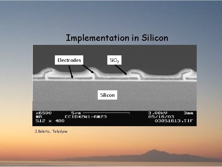
Implementation in Silicon Electrodes Si. O 2 Silicon J. Beletic, Teledyne

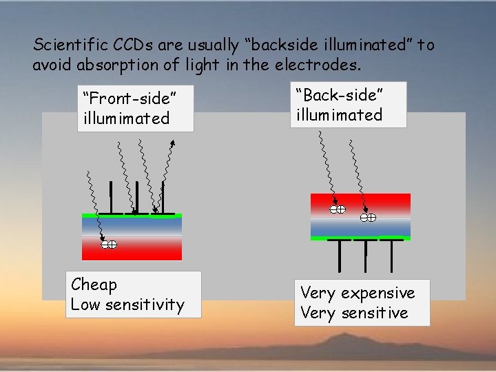
Scientific CCDs are usually “backside illuminated” to avoid absorption of light in the electrodes. “Front-side” illumimated Cheap Low sensitivity “Back-side” illumimated Very expensive Very sensitive

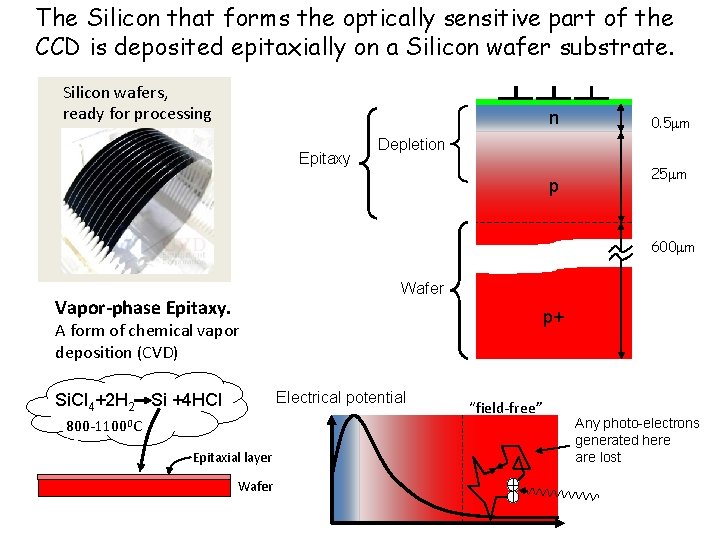
The Silicon that forms the optically sensitive part of the CCD is deposited epitaxially on a Silicon wafer substrate. Silicon wafers, ready for processing n Epitaxy 0. 5 mm Depletion p 25 mm 600 mm Wafer Vapor-phase Epitaxy. p+ A form of chemical vapor deposition (CVD) Electrical potential Si. Cl 4+2 H 2 - Si +4 HCl 800 -11000 C Epitaxial layer Wafer “field-free” Any photo-electrons generated here are lost

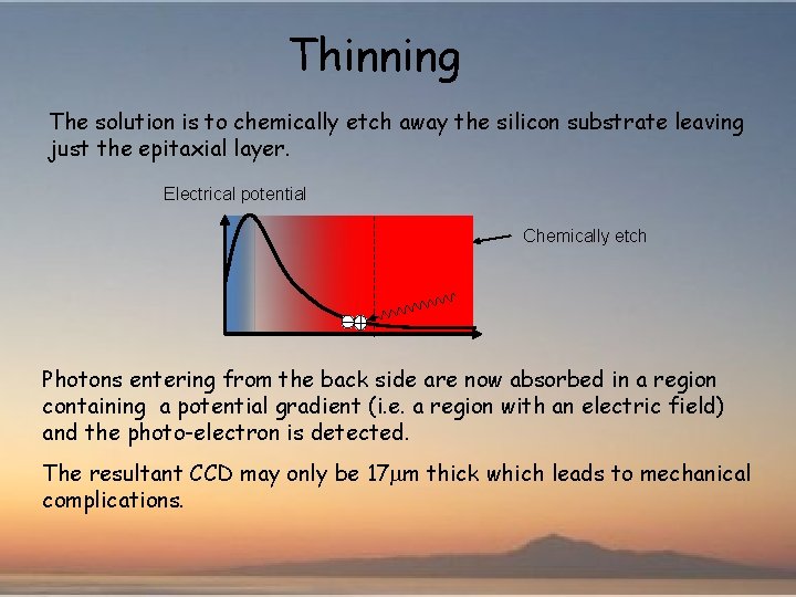
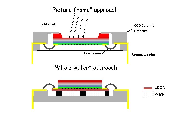
Thinning The solution is to chemically etch away the silicon substrate leaving just the epitaxial layer. Electrical potential Chemically etch Photons entering from the back side are now absorbed in a region containing a potential gradient (i. e. a region with an electric field) and the photo-electron is detected. The resultant CCD may only be 17 mm thick which leads to mechanical complications.

“Picture frame” approach Light input CCD Ceramic package Bond wires Connector pins “Whole wafer” approach Epoxy Wafer

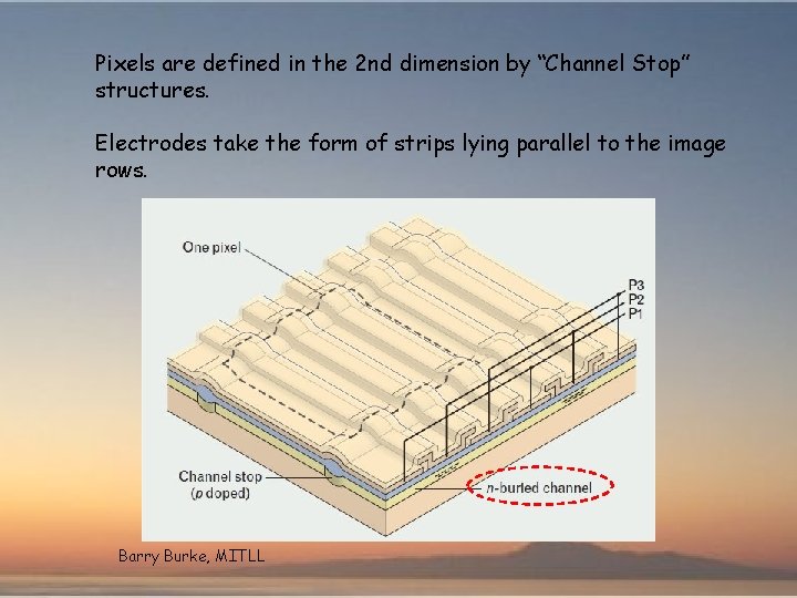
Pixels are defined in the 2 nd dimension by “Channel Stop” structures. Electrodes take the form of strips lying parallel to the image rows. J. Beletic, Teledyne Barry Burke, MITLL

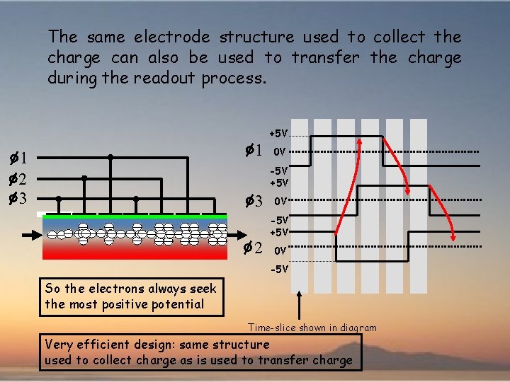
The same electrode structure used to collect the charge can also be used to transfer the charge during the readout process. +5 V 1 1 2 3 0 V -5 V +5 V 3 2 0 V -5 V +5 V 0 V -5 V So the electrons always seek the most positive potential Time-slice shown in diagram Very efficient design: same structure used to collect charge as is used to transfer charge

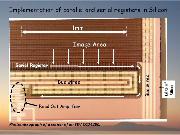
A second “conveyor belt” at right angles to the first is required to transfer each row, pixel at a time to the output amplifier. This is known as the serial register. Image Area Also described as the parallel register Serial Register. Also widely described as: “The register” or ”The horizontal register” On-chip amplifier at end of the serial register. This converts the pixel charge into a voltage

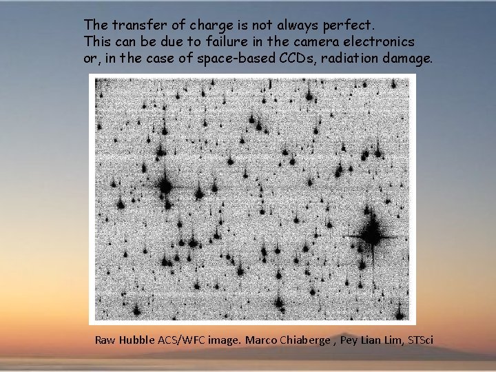
The transfer of charge is not always perfect. This can be due to failure in the camera electronics or, in the case of space-based CCDs, radiation damage. Raw Hubble ACS/WFC image. Marco Chiaberge , Pey Lian Lim, STSci

Implementation of parallel and serial registers in Silicon 1 mm Image Area Read Out Amplifier Photomicrograph of a corner of an EEV CCD 4280. Edge of Silicon Bus wires Serial Register

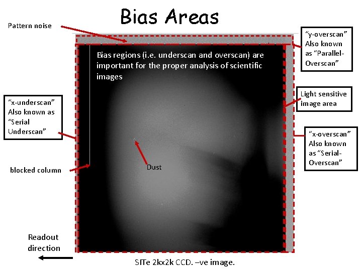
Pattern noise Bias Areas Bias regions (i. e. underscan and overscan) are important for the proper analysis of scientific images Light sensitive image area “x-underscan” Also known as “Serial Underscan” blocked column “y-overscan” Also known as “Parallel. Overscan” Dust Readout direction SITe 2 kx 2 k CCD. –ve image. “x-overscan” Also known as “Serial. Overscan”

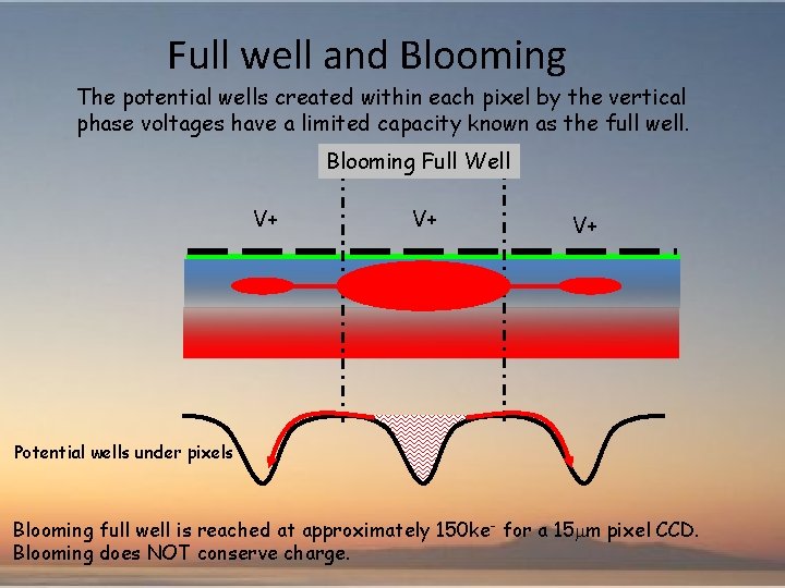
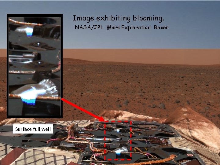
Full well and Blooming The potential wells created within each pixel by the vertical phase voltages have a limited capacity known as the full well. Blooming Surface Full Well V+ V+ V+ Potential wells under pixels Blooming full well is reached at approximately 150 ke - for a 15 mm pixel CCD. Blooming does NOT conserve charge.

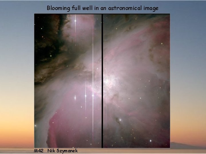
Blooming full well in an astronomical image M 42 Nik Szymanek

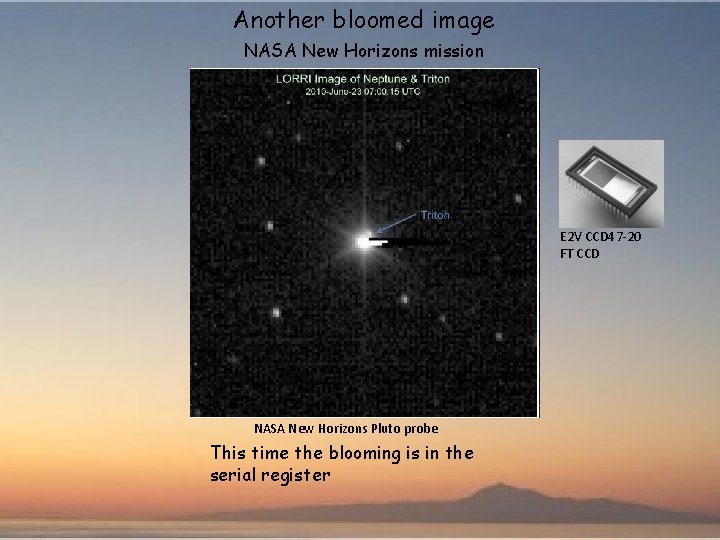
Another bloomed image NASA New Horizons mission E 2 V CCD 47 -20 FT CCD NASA New Horizons Pluto probe This time the blooming is in the serial register

Image exhibiting blooming. NASA/JPL Mars Exploration Rover Surface full well

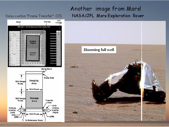
Another image from Mars! Dalsa custom “Frame Transfer” CCD NASA/JPL Mars Exploration Rover Blooming full well

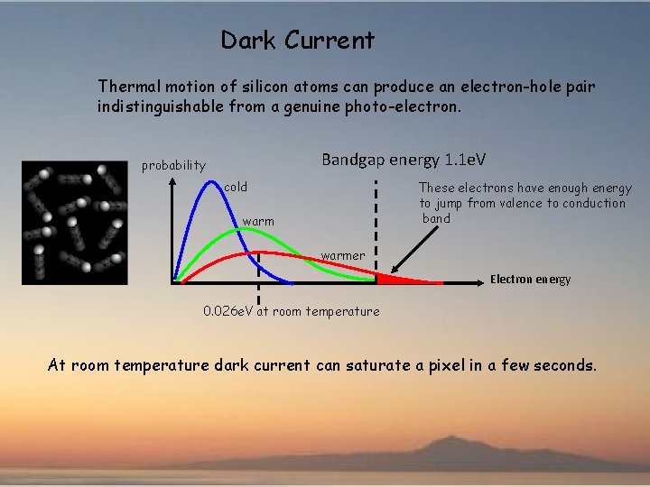
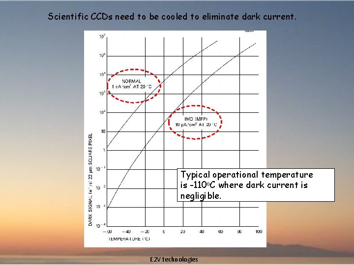
Dark Current Thermal motion of silicon atoms can produce an electron-hole pair indistinguishable from a genuine photo-electron. Bandgap energy 1. 1 e. V probability cold These electrons have enough energy to jump from valence to conduction band warmer Electron energy 0. 026 e. V at room temperature At room temperature dark current can saturate a pixel in a few seconds.

Scientific CCDs need to be cooled to eliminate dark current. Typical operational temperature is -110 o. C where dark current is negligible. E 2 V technologies

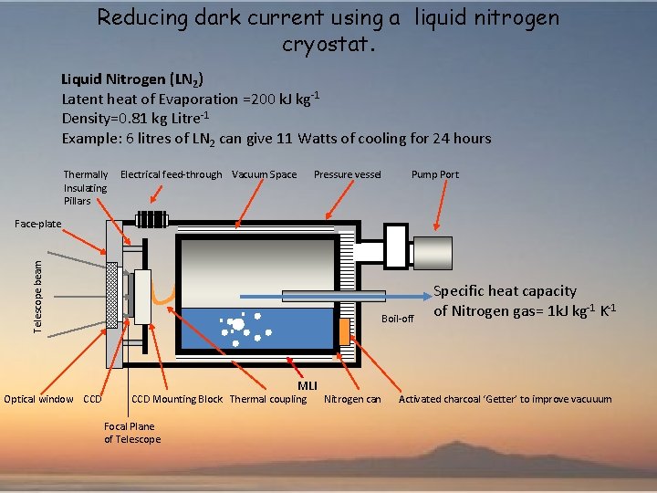
Reducing dark current using a liquid nitrogen cryostat. Liquid Nitrogen (LN 2) Latent heat of Evaporation =200 k. J kg-1 Density=0. 81 kg Litre-1 Example: 6 litres of LN 2 can give 11 Watts of cooling for 24 hours Thermally Insulating Pillars Electrical feed-through Vacuum Space Pressure vessel Pump Port Telescope beam Face-plate Optical window CCD . . . Boil-off MLI CCD Mounting Block Thermal coupling Focal Plane of Telescope Nitrogen can Specific heat capacity of Nitrogen gas= 1 k. J kg-1 K-1 Activated charcoal ‘Getter’ to improve vacuuum

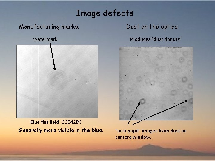
Image defects Manufacturing marks. watermark Dust on the optics. Produces “dust donuts” Blue flat field CCD 4280 Generally more visible in the blue. “anti-pupil” images from dust on camera window.

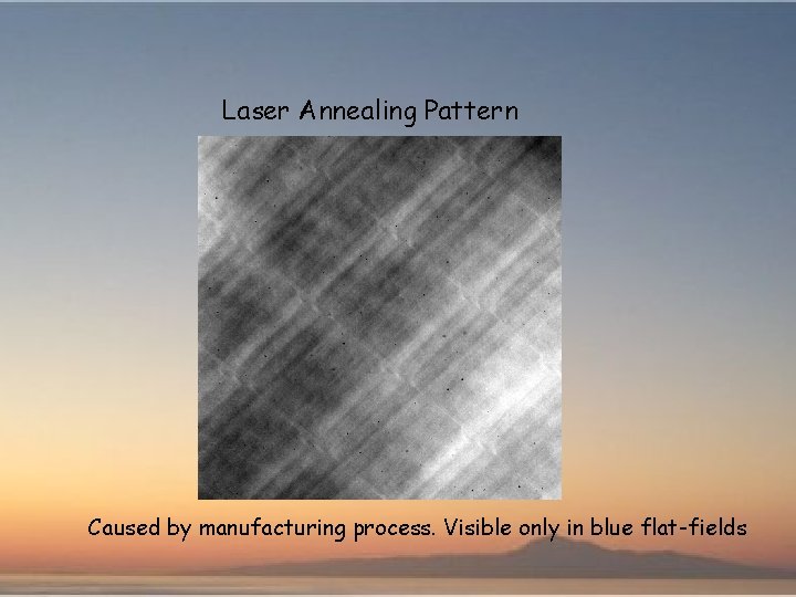
Laser Annealing Pattern Caused by manufacturing process. Visible only in blue flat-fields

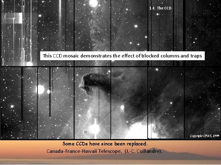
1. 4. The CCD This CCD mosaic demonstrates the effect of blocked columns and traps Some CCDs have since been replaced. Canada-France-Hawaii Telescope. (J. -C. Cuillandre).

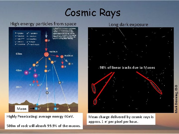
Cosmic Rays High energy particles from space Long dark exposure Mark Downing, ESO 98% of linear tracks due to Muons Muon Highly Penetrating: average energy 4 Ge. V. 500 m of rock will absorb 99. 9% of the muons. Mean charge delivered by cosmic rays is approx. 1 e- per pixel per hour.

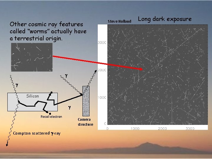
Other cosmic ray features called “worms” actually have a terrestrial origin. g g Silicon g Recoil electron Compton scattered g-ray Camera structure Steve Holland Long dark exposure

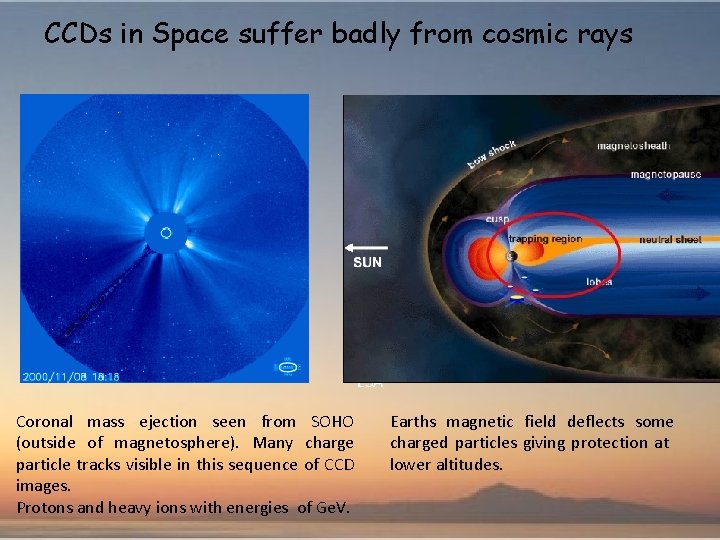
CCDs in Space suffer badly from cosmic rays ESA Coronal mass ejection seen from SOHO (outside of magnetosphere). Many charge particle tracks visible in this sequence of CCD images. Protons and heavy ions with energies of Ge. V. Earths magnetic field deflects some charged particles giving protection at lower altitudes.

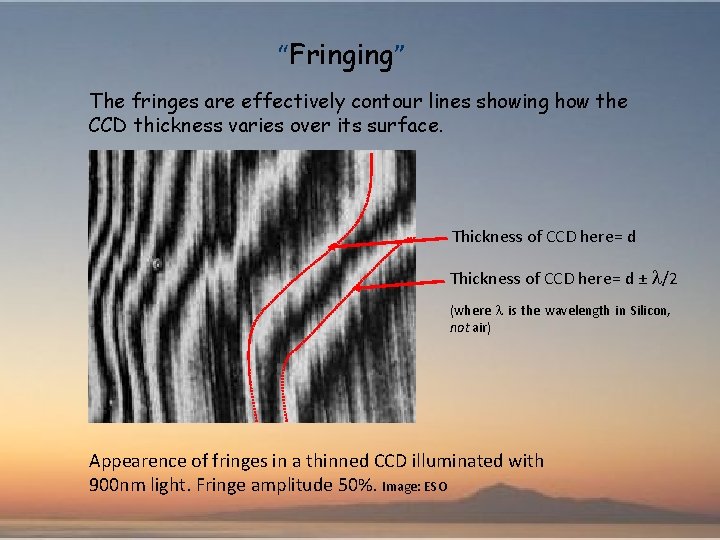
“Fringing” The fringes are effectively contour lines showing how the CCD thickness varies over its surface. Thickness of CCD here= d ± l/2 (where l is the wavelength in Silicon, not air) Appearence of fringes in a thinned CCD illuminated with 900 nm light. Fringe amplitude 50%. Image: ESO

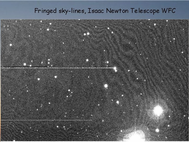
Fringed sky-lines, Isaac Newton Telescope WFC

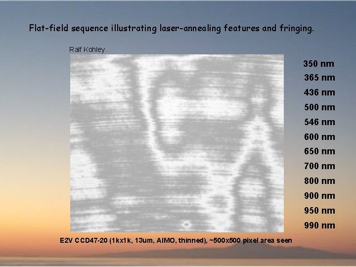
Flat-field sequence illustrating laser-annealing features and fringing. Ralf Kohley. 350 nm 365 nm 436 nm 500 nm 546 nm 600 nm 650 nm 700 nm 800 nm 950 nm 990 nm E 2 V CCD 47 -20 (1 kx 1 k, 13 um, AIMO, thinned), ~500 x 500 pixel area seen

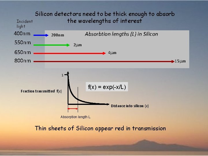
Incident light 400 nm Silicon detectors need to be thick enough to absorb the wavelengths of interest Absorbtion lengths (L) in Silicon 200 nm 550 nm 2 mm 650 nm 800 nm 4 mm 15 mm 1 Fraction transmitted f(x) = exp(-x/L) Distance into silicon (x) Absorption length L Thin sheets of Silicon appear red in transmission

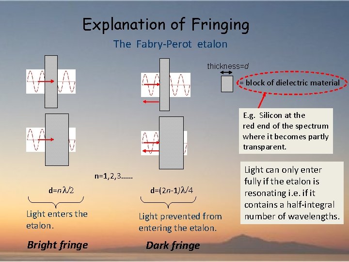
Explanation of Fringing The Fabry-Perot etalon thickness=d = block of dielectric material E. g. Silicon at the red end of the spectrum where it becomes partly transparent. n=1, 2, 3…… d=nl/2 Light enters the etalon. Bright fringe d=(2 n-1)l/4 Light prevented from entering the etalon. Dark fringe Light can only enter fully if the etalon is resonating i. e. if it contains a half-integral number of wavelengths.

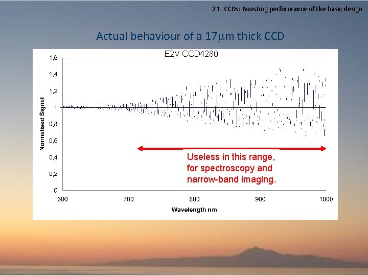
2. 1. CCDs: Boosting performance of the basic design Actual behaviour of a 17 mm thick CCD E 2 V CCD 4280 Useless in this range, for spectroscopy and narrow-band imaging.

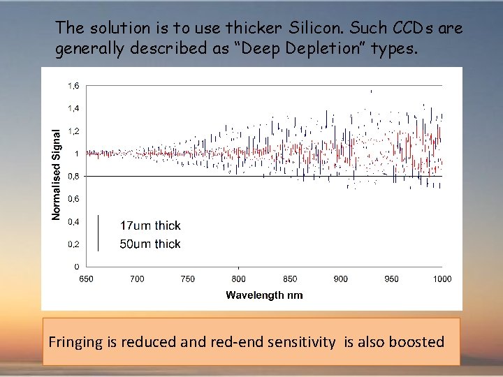
The solution is to use thicker Silicon. Such CCDs are generally described as “Deep Depletion” types. Fringing is reduced and red-end sensitivity is also boosted

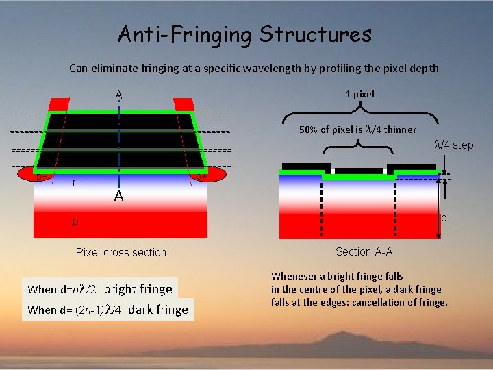
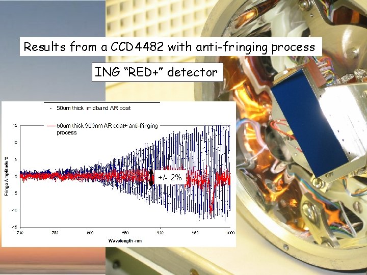
Anti-Fringing Structures Can eliminate fringing at a specific wavelength by profiling the pixel depth 1 pixel A 50% of pixel is l/4 thinner l/4 step p+ p+ n A d p Pixel cross section When d=nl/2 bright fringe When d= (2 n-1)l/4 dark fringe Section A-A Whenever a bright fringe falls in the centre of the pixel, a dark fringe falls at the edges: cancellation of fringe.

Results from a CCD 4482 with anti-fringing process ING “RED+” detector +/- 2%

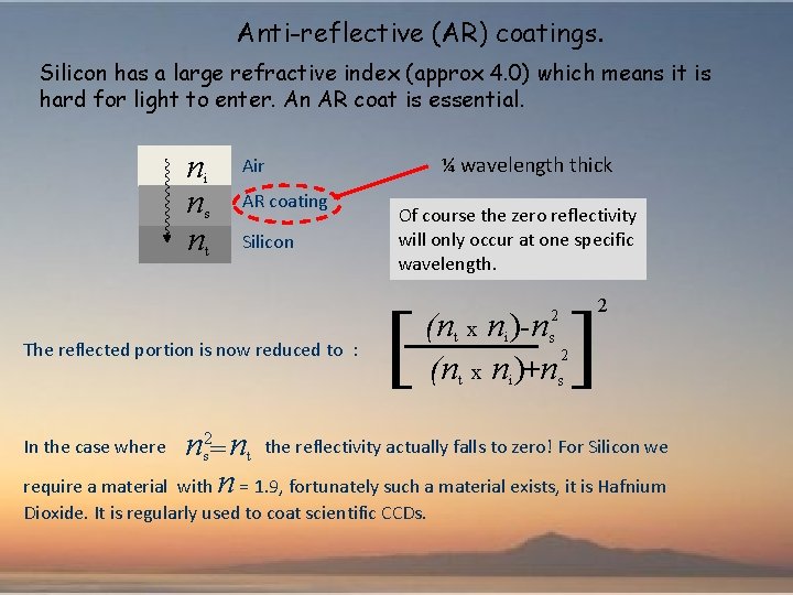
Anti-reflective (AR) coatings. Silicon has a large refractive index (approx 4. 0) which means it is hard for light to enter. An AR coat is essential. ni ns nt ¼ wavelength thick Air AR coating Silicon The reflected portion is now reduced to : Of course the zero reflectivity will only occur at one specific wavelength. [ (nt x ni)-ns 2 (nt x ni)+ns 2 ] 2 ns 2= nt the reflectivity actually falls to zero! For Silicon we require a material with n = 1. 9, fortunately such a material exists, it is Hafnium In the case where Dioxide. It is regularly used to coat scientific CCDs.

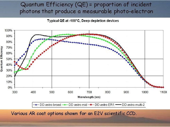
Quantum Efficiency (QE) = proportion of incident photons that produce a measurable photo-electron Various AR coat options shown for an E 2 V scientific CCD.

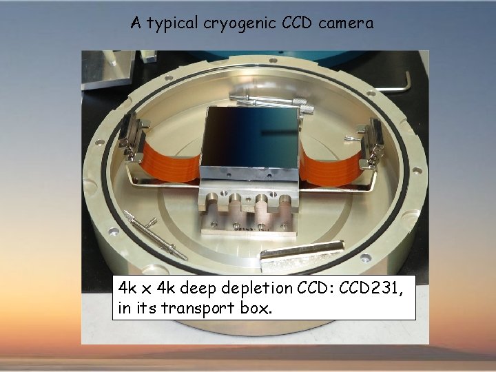
A typical cryogenic CCD camera 4 k x 4 k deep depletion CCD: CCD 231, in its transport box.

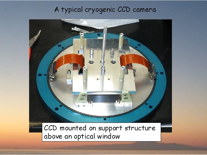
A typical cryogenic CCD camera CCD mounted on support structure above an optical window

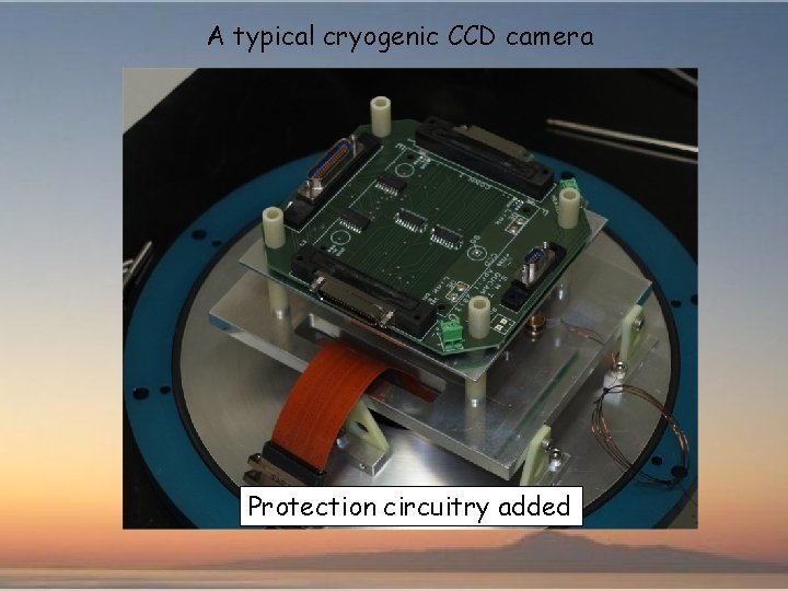
A typical cryogenic CCD camera Protection circuitry added

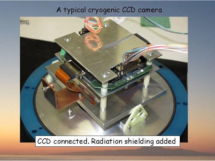
A typical cryogenic CCD camera CCD connected. Radiation shielding added

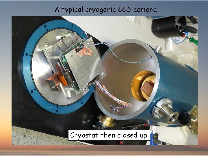
A typical cryogenic CCD camera Cryostat then closed up

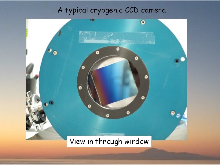
A typical cryogenic CCD camera View in through window

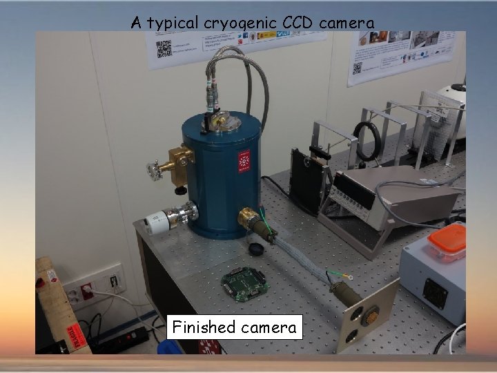
A typical cryogenic CCD camera Finished camera

End of Presentation