Active Pixel Sensors in highvoltage CMOS technologies for






- Slides: 57

Active Pixel Sensors in high-voltage CMOS technologies for ATLAS Ivan Perić University of Heidelberg, Germany Ivan Peric, WIT 2012 1

Introduction: High-Voltage CMOS Pixel Detectors Ivan Peric, WIT 2012 2

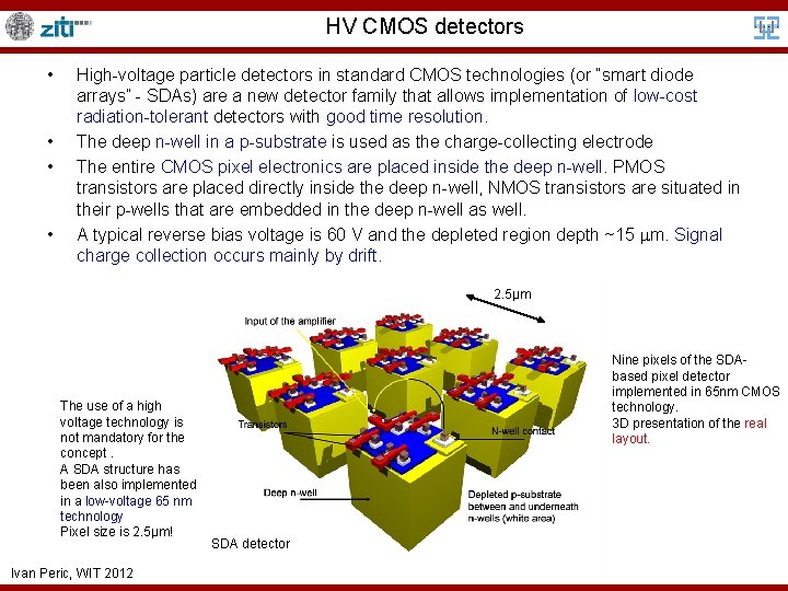
HV CMOS detectors • • High-voltage particle detectors in standard CMOS technologies (or “smart diode arrays” - SDAs) are a new detector family that allows implementation of low-cost radiation-tolerant detectors with good time resolution. The deep n-well in a p-substrate is used as the charge-collecting electrode The entire CMOS pixel electronics are placed inside the deep n-well. PMOS transistors are placed directly inside the deep n-well, NMOS transistors are situated in their p-wells that are embedded in the deep n-well as well. A typical reverse bias voltage is 60 V and the depleted region depth ~15 m. Signal charge collection occurs mainly by drift. 2. 5µm The use of a high voltage technology is not mandatory for the concept. A SDA structure has been also implemented in a low-voltage 65 nm technology Pixel size is 2. 5µm! Ivan Peric, WIT 2012 Nine pixels of the SDAbased pixel detector implemented in 65 nm CMOS technology. 3 D presentation of the real layout. SDA detector

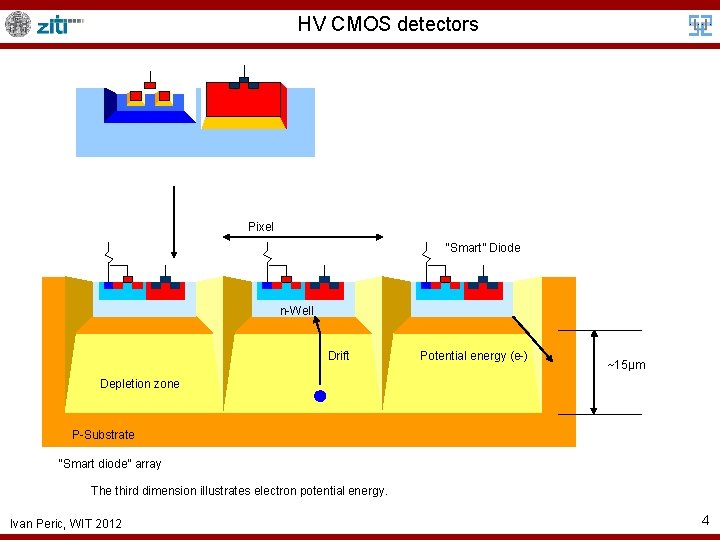
HV CMOS detectors Pixel “Smart” Diode n-Well Drift Potential energy (e-) ~15µm Depletion zone P-Substrate “Smart diode” array The third dimension illustrates electron potential energy. Ivan Peric, WIT 2012 4

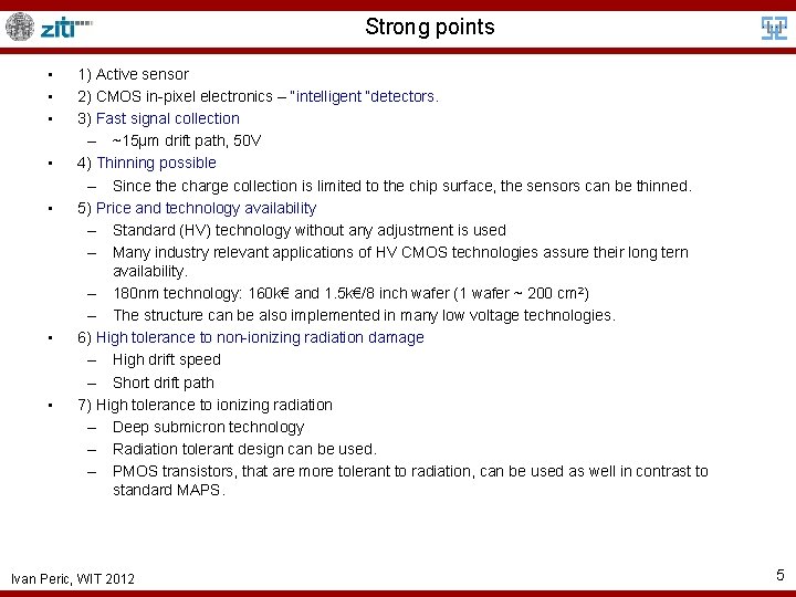
Strong points • • 1) Active sensor 2) CMOS in-pixel electronics – “intelligent “detectors. 3) Fast signal collection – ~15μm drift path, 50 V 4) Thinning possible – Since the charge collection is limited to the chip surface, the sensors can be thinned. 5) Price and technology availability – Standard (HV) technology without any adjustment is used – Many industry relevant applications of HV CMOS technologies assure their long tern availability. – 180 nm technology: 160 k€ and 1. 5 k€/8 inch wafer (1 wafer ~ 200 cm 2) – The structure can be also implemented in many low voltage technologies. 6) High tolerance to non-ionizing radiation damage – High drift speed – Short drift path 7) High tolerance to ionizing radiation – Deep submicron technology – Radiation tolerant design can be used. – PMOS transistors, that are more tolerant to radiation, can be used as well in contrast to standard MAPS. Ivan Peric, WIT 2012 5

Capacitive Coupled Pixel Detectors - CCPDs Ivan Peric, WIT 2012 6

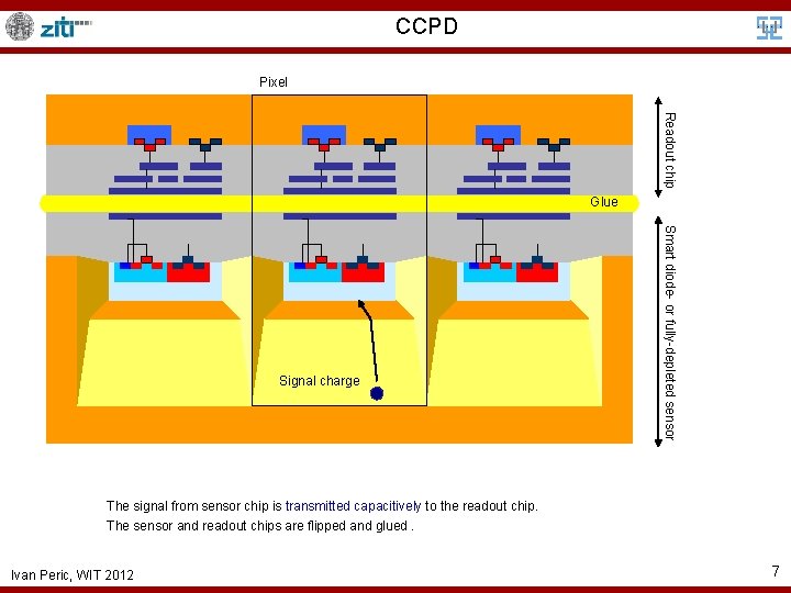
CCPD Pixel Readout chip Glue Smart diode- or fully-depleted sensor Signal charge The signal from sensor chip is transmitted capacitively to the readout chip. The sensor and readout chips are flipped and glued. Ivan Peric, WIT 2012 7

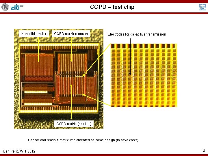
CCPD – test chip Monolithic matrix CCPD matrix (sensor) Electrodes for capacitive transmission CCPD matrix (readout) Sensor and readout matrix implemented as same design (to save costs) Ivan Peric, WIT 2012 8

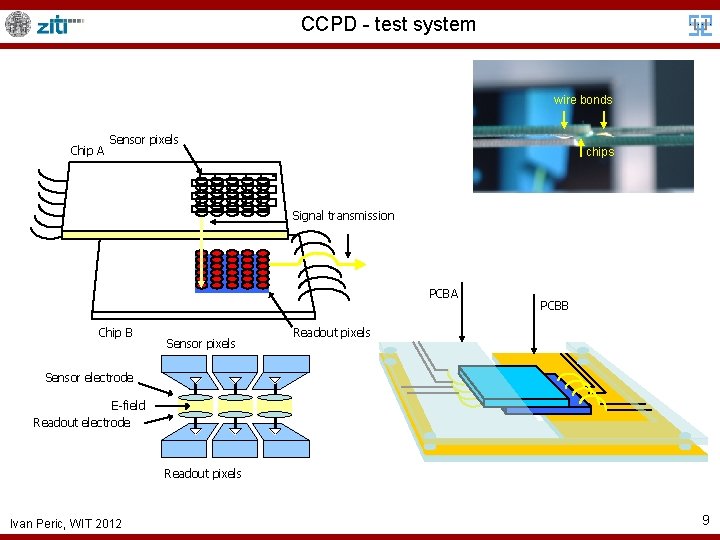
CCPD - test system wire bonds Chip A Sensor pixels chips Signal transmission PCBA Chip B Sensor pixels PCBB Readout pixels Sensor electrode E-field Readout electrode Readout pixels Ivan Peric, WIT 2012 9

High-Voltage CMOS Detectors for ATLAS Ivan Peric, WIT 2012 10

CCPD Concept Ivan Peric, WIT 2012 11

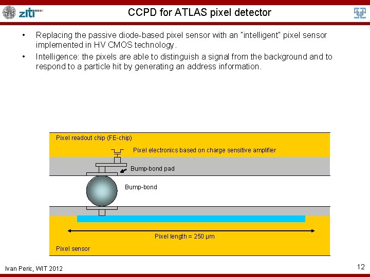
CCPD for ATLAS pixel detector • • Replacing the passive diode-based pixel sensor with an “intelligent” pixel sensor implemented in HV CMOS technology. Intelligence: the pixels are able to distinguish a signal from the background and to respond to a particle hit by generating an address information. Pixel readout chip (FE-chip) Pixel electronics based on charge sensitive amplifier Bump-bond pad Bump-bond Pixel length = 250 μm Pixel sensor Ivan Peric, WIT 2012 12

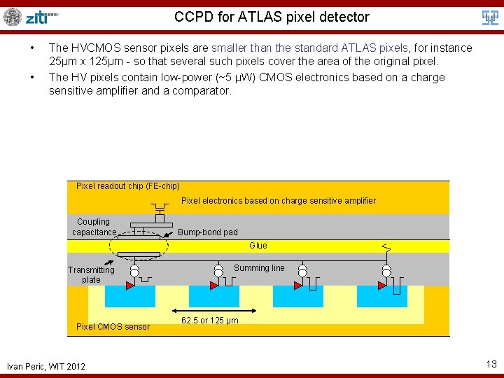
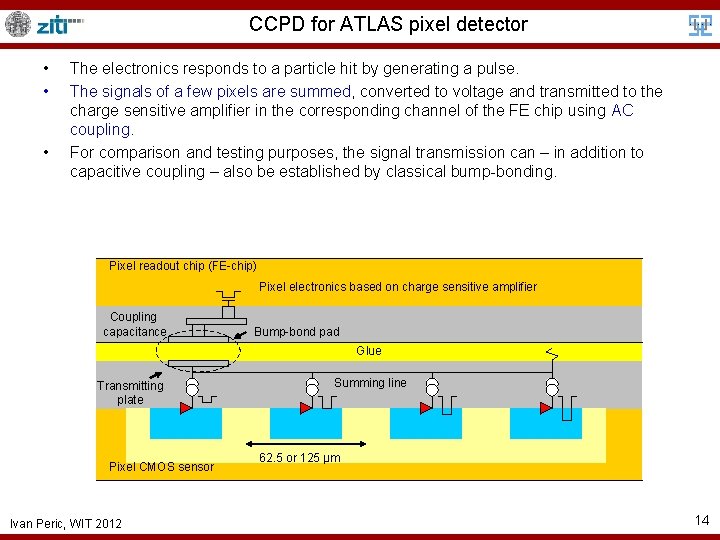
CCPD for ATLAS pixel detector • • The HVCMOS sensor pixels are smaller than the standard ATLAS pixels, for instance 25μm x 125μm - so that several such pixels cover the area of the original pixel. The HV pixels contain low-power (~5 μW) CMOS electronics based on a charge sensitive amplifier and a comparator. Pixel readout chip (FE-chip) Pixel electronics based on charge sensitive amplifier Coupling capacitance Bump-bond pad Glue Transmitting plate Pixel CMOS sensor Ivan Peric, WIT 2012 Summing line 62. 5 or 125 μm 13

CCPD for ATLAS pixel detector • • • The electronics responds to a particle hit by generating a pulse. The signals of a few pixels are summed, converted to voltage and transmitted to the charge sensitive amplifier in the corresponding channel of the FE chip using AC coupling. For comparison and testing purposes, the signal transmission can – in addition to capacitive coupling – also be established by classical bump-bonding. Pixel readout chip (FE-chip) Pixel electronics based on charge sensitive amplifier Coupling capacitance Bump-bond pad Glue Transmitting plate Pixel CMOS sensor Ivan Peric, WIT 2012 Summing line 62. 5 or 125 μm 14

CCPD for ATLAS pixel detector • • Each of the pixels that couple to one FE receiver can have its unique signal amplitude, so that the pixel can be identified by examining the amplitude information generated in FE chip. In this way, spatial resolution in - and z-direction can be improved. Ivan Peric, WIT 2012 15

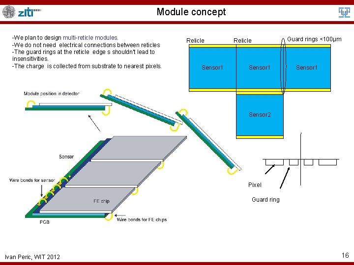
Module concept -We plan to design multi-reticle modules. -We do not need electrical connections between reticles -The guard rings at the reticle edge s shouldn‘t lead to insensitivities. -The charge is collected from substrate to nearest pixels. Relicle Sensor 1 Guard rings <100µm Relicle Sensor 1 Sensor 2 Pixel Guard ring Ivan Peric, WIT 2012 16

Advantages compared to existing detectors • • No need for bump-bond connection between the sensor and readout chip – lower price, better mechanical stability, less material Commercial sensor technology – lower price No need for bias voltages higher than 60 V Operation at temperatures above 0 C is according to tests possible (irradiations to 1015 neq/cm 2) Increased spatial resolution (e. g. 25 m x 125 m binary resolution) with the existing FE chip Smaller clusters at high incidence angles Possibility of sensor-thinning without signal loss. Since we do not use bumps and FE chips can be thinned as well, the amount of material would be very low. Interesting choice for other experiments where low-mass detectors are needed such as CLIC, ILC, CBM, etc. . . Ivan Peric, WIT 2012 17

Strip-like Concept Ivan Peric, WIT 2012 18

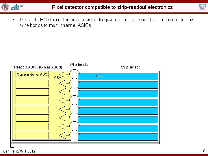
Pixel detector compatible to strip-readout electronics • Present LHC strip detectors consist of large-area strip sensors that are connected by wire bonds to multi-channel ASICs. Readout ASIC (such as ABCN) Comparator or ADC Ivan Peric, WIT 2012 CSA Wire-bonds Strip sensor Strip 19

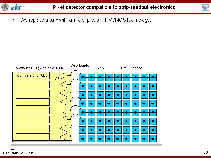
Pixel detector compatible to strip-readout electronics • We replace a strip with a line of pixels in HVCMOS technology. Readout ASIC (such as ABCN) Comparator or ADC Ivan Peric, WIT 2012 Wire-bonds Pixels CMOS sensor CSA 20

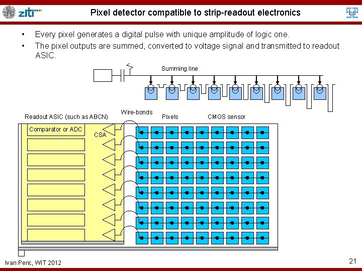
Pixel detector compatible to strip-readout electronics • • Every pixel generates a digital pulse with unique amplitude of logic one. The pixel outputs are summed, converted to voltage signal and transmitted to readout ASIC. Summing line Readout ASIC (such as ABCN) Comparator or ADC Ivan Peric, WIT 2012 Wire-bonds Pixels CMOS sensor CSA 21

Pixel detector compatible to strip-readout electronics • • A large area CMOS sensor can be produced by stitching several 2 cm x 2 cm wafer reticles. Any arbitrary pixel group pattern is possible. Advantages: Commercial sensor technology – lower price per unit area Intrinsic 2 D spatial resolution (e. g. 25 m x 125 m binary resolution) No need for bias voltages higher than 60 V Operation at temperatures above 0 C is according to tests possible (irradiations to 1015 neq/cm 2) Thinning possible Ivan Peric, WIT 2012 22

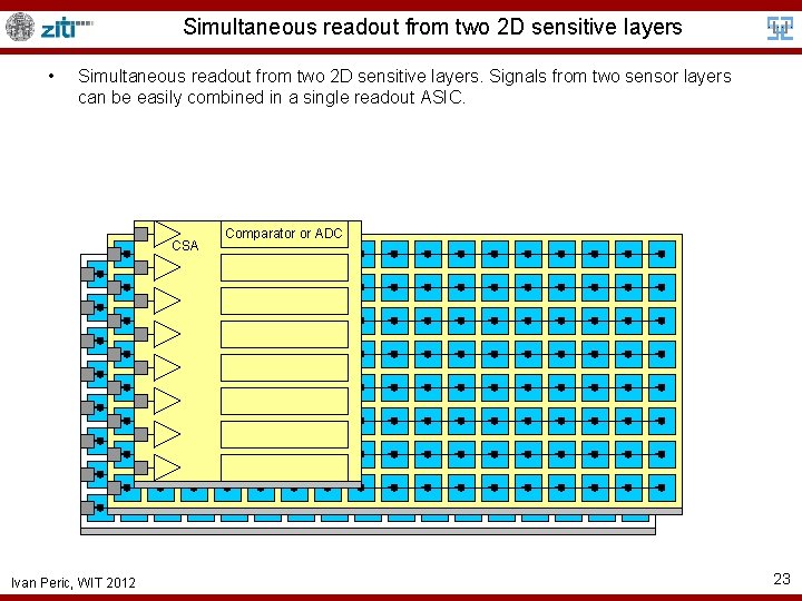
Simultaneous readout from two 2 D sensitive layers • Simultaneous readout from two 2 D sensitive layers. Signals from two sensor layers can be easily combined in a single readout ASIC. CSA Ivan Peric, WIT 2012 Comparator or ADC 23

Test Chip HV 2 FEI 4 Ivan Peric, WIT 2012 24

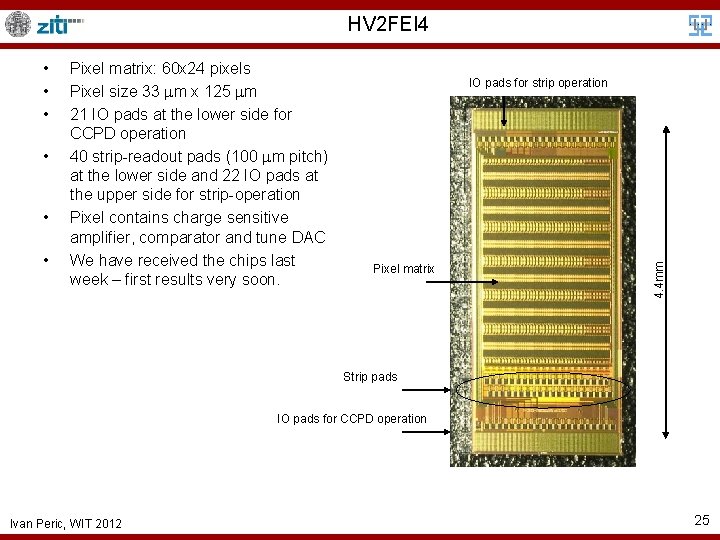
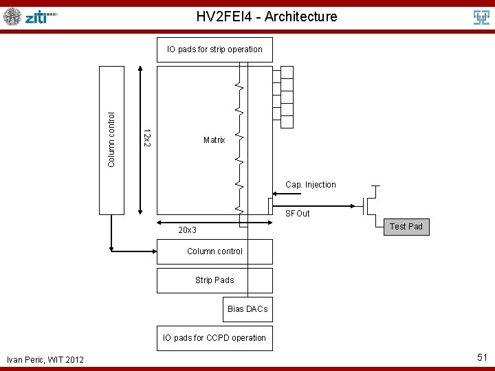
HV 2 FEI 4 • • • Pixel matrix: 60 x 24 pixels Pixel size 33 m x 125 m 21 IO pads at the lower side for CCPD operation 40 strip-readout pads (100 m pitch) at the lower side and 22 IO pads at the upper side for strip-operation Pixel contains charge sensitive amplifier, comparator and tune DAC We have received the chips last week – first results very soon. IO pads for strip operation Pixel matrix 4. 4 mm • • • Strip pads IO pads for CCPD operation Ivan Peric, WIT 2012 25

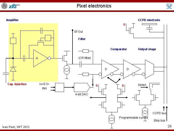
Pixel electronics Amplifier CCPD electrode G SFOut Filter Comparator (CR filter) A D Cap. Injection Output stage In<0: 3> RW G D G Select 4 -bit DAC CCPD bus Programmable current Ivan Peric, WIT 2012 Strip bus 26

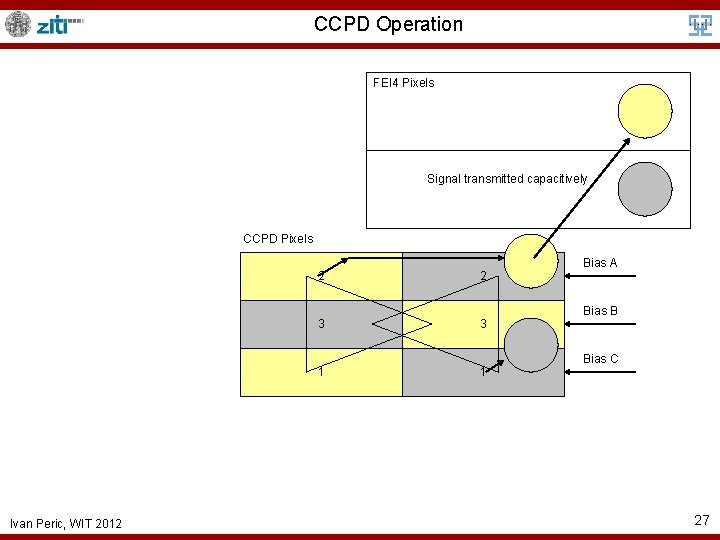
CCPD Operation FEI 4 Pixels Signal transmitted capacitively CCPD Pixels 2 3 1 Ivan Peric, WIT 2012 2 3 1 Bias A Bias B Bias C 27

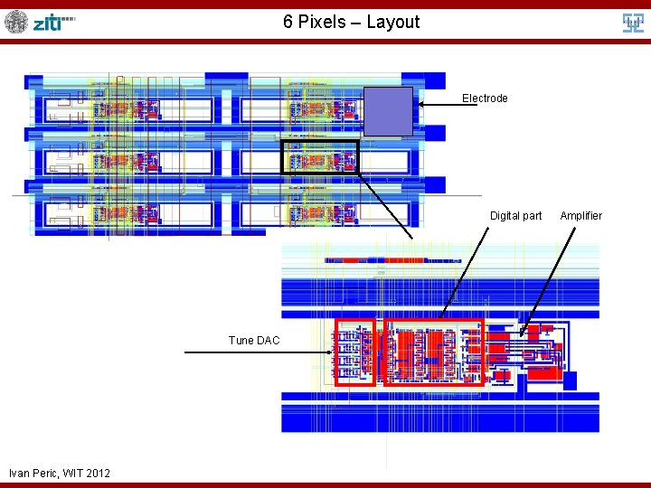
6 Pixels – Layout Electrode Digital part Tune DAC Ivan Peric, WIT 2012 Amplifier

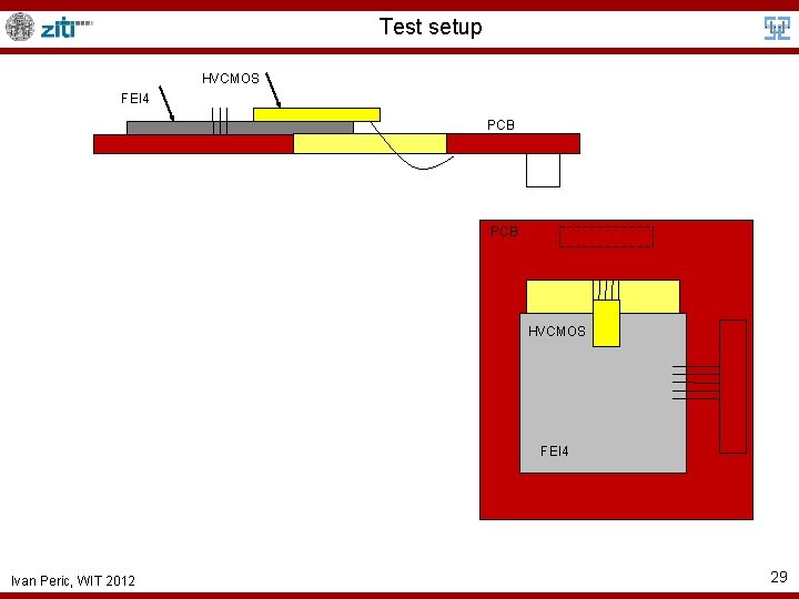
Test setup HVCMOS FEI 4 PCB HVCMOS FEI 4 Ivan Peric, WIT 2012 29

Experimental Results with other Prototypes Ivan Peric, WIT 2012 30

Efficiency and Signal Amplitude Ivan Peric, WIT 2012 31

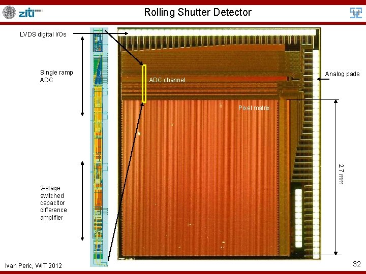
Rolling Shutter Detector LVDS digital I/Os Single ramp ADC Analog pads ADC channel Pixel matrix 2. 7 mm 2 -stage switched capacitor difference amplifier Ivan Peric, WIT 2012 32

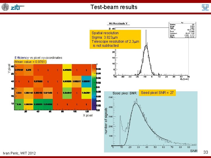
Test-beam results Spatial resolution Sigma: 3. 823 m Telescope resolution of 2. 3 m is not subtracted Y pixel Efficiency vs pixel xy-coordinates (Mean value = 0. 9761) Seed pixel SNR = 27 X pixel Ivan Peric, WIT 2012 33

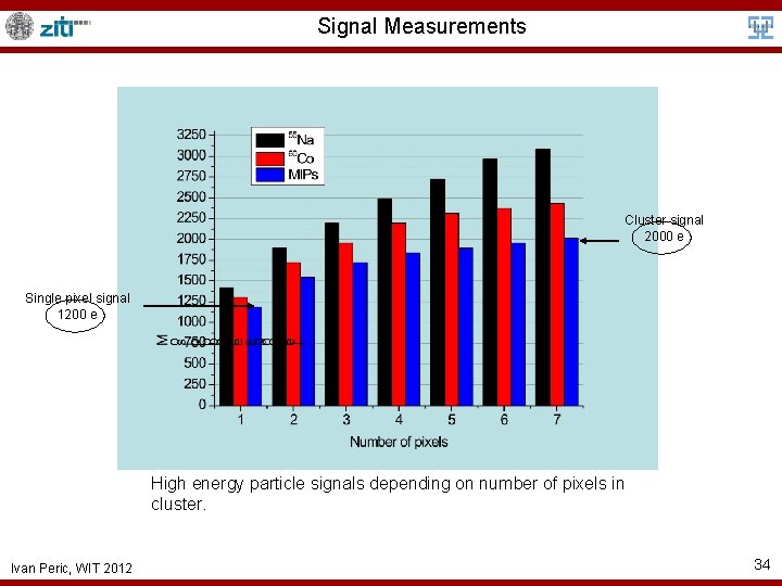
Signal Measurements Cluster signal 2000 e Single pixel signal 1200 e High energy particle signals depending on number of pixels in cluster. Ivan Peric, WIT 2012 34

CCPD Operation Ivan Peric, WIT 2012 35

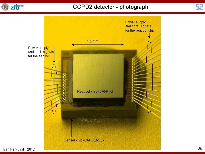
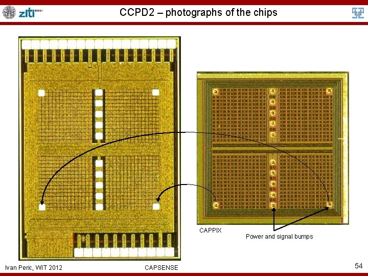
CCPD 2 detector - photograph Power supply and cont. signals for the readout chip 1. 5 mm Power supply and cont. signals for the sensor Readout chip (CAPPIX) Sensor chip (CAPSENSE) Ivan Peric, WIT 2012 36

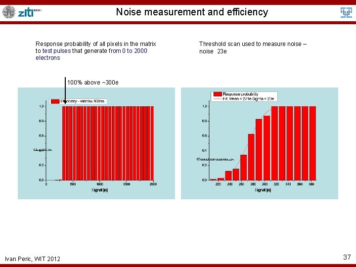
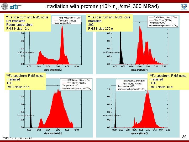
Noise measurement and efficiency Response probability of all pixels in the matrix to test pulses that generate from 0 to 2000 electrons Threshold scan used to measure noise – noise 23 e 100% above ~300 e Ivan Peric, WIT 2012 37

Radiation Tolerance (CCPD 2 Sensor) Ivan Peric, WIT 2012 38

Irradiation with protons (1015 neq/cm 2, 300 MRad) 55 Fe spectrum and RMS noise Not irradiated Room temperature RMS Noise 12 e 55 Fe spectrum, RMS noise Irradiated 10 C RMS Noise 77 e Ivan Peric, WIT 2012 55 Fe spectrum and RMS noise Irradiated 20 C RMS Noise 270 e 55 Fe spectrum, RMS noise Irradiated -10 C RMS Noise 40 e 39

Time Resolution Ivan Peric, WIT 2012 40

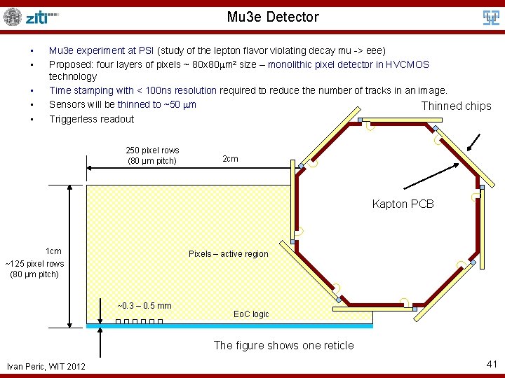
Mu 3 e Detector • • • Mu 3 e experiment at PSI (study of the lepton flavor violating decay mu -> eee) Proposed: four layers of pixels ~ 80 x 80 m 2 size – monolithic pixel detector in HVCMOS technology Time stamping with < 100 ns resolution required to reduce the number of tracks in an image. Sensors will be thinned to ~50 m Thinned chips Triggerless readout 250 pixel rows (80 μm pitch) 2 cm Kapton PCB 1 cm Pixels – active region ~125 pixel rows (80 μm pitch) ~0. 3 – 0. 5 mm Eo. C logic The figure shows one reticle Ivan Peric, WIT 2012 41

Mu 3 e Detector • • More details can be seen in poster session: Dirk Wiedner: “A tracker for the novel mu 3 e experiment based on high voltage monolithic active pixel sensors” Ivan Peric, WIT 2012 42

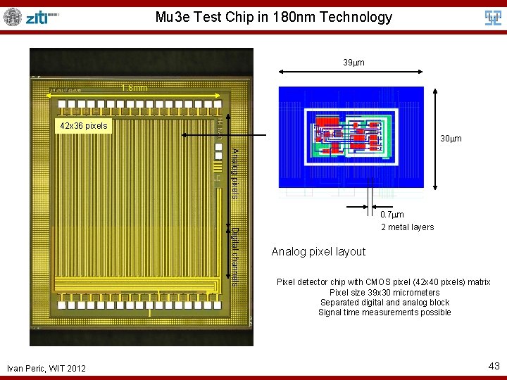
Mu 3 e Test Chip in 180 nm Technology 39 m 1. 8 mm 42 x 36 pixels 30 m Analog pixels Digital channels Ivan Peric, WIT 2012 0. 7 m 2 metal layers Analog pixel layout Pixel detector chip with CMOS pixel (42 x 40 pixels) matrix Pixel size 39 x 30 micrometers Separated digital and analog block Signal time measurements possible 43

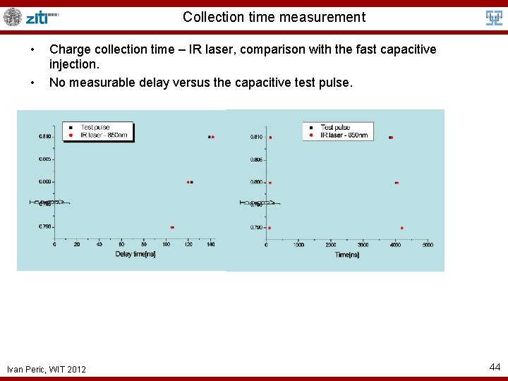
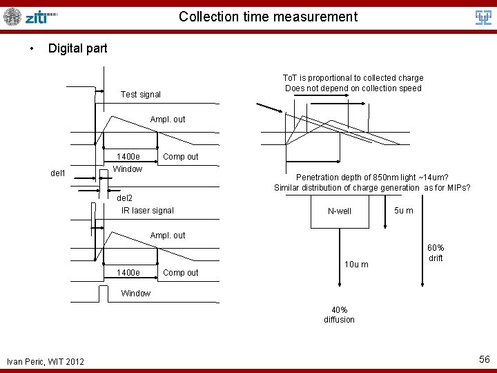
Collection time measurement • • Charge collection time – IR laser, comparison with the fast capacitive injection. No measurable delay versus the capacitive test pulse. Ivan Peric, WIT 2012 44

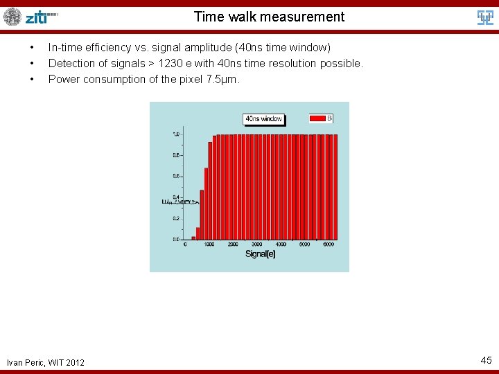
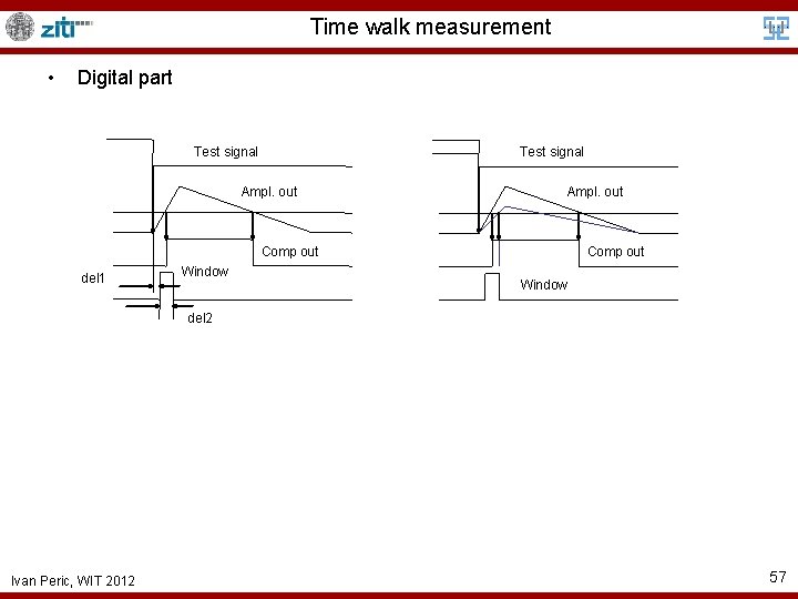
Time walk measurement • • • In-time efficiency vs. signal amplitude (40 ns time window) Detection of signals > 1230 e with 40 ns time resolution possible. Power consumption of the pixel 7. 5µm. Ivan Peric, WIT 2012 45

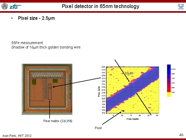
Pixel detector in 65 nm technology • Pixel size - 2. 5µm 55 Fe measurement Shadow of 16 m thick golden bonding wire 16µm Pixel matrix (32 x 256) Pixel Ivan Peric, WIT 2012 46

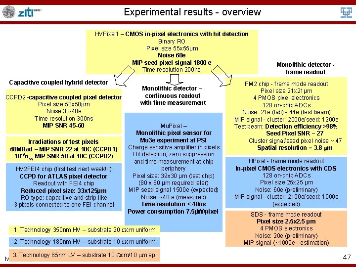
Experimental results - overview HVPixel 1 – CMOS in-pixel electronics with hit detection Binary RO Pixel size 55 x 55μm Noise 60 e MIP seed pixel signal 1800 e Time resolution 200 ns Capacitive coupled hybrid detector CCPD 2 -capacitive coupled pixel detector Pixel size 50 x 50μm Noise 30 -40 e Time resolution 300 ns MIP SNR 45 -60 Irradiations of test pixels 60 MRad – MIP SNR 22 at 10 C (CCPD 1) 1015 neq MIP SNR 50 at 10 C (CCPD 2) HV 2 FEI 4 chip (first test next week!!!) CCPD for ATLAS pixel detector Readout with FEI 4 chip Reduced pixel size: 33 x 125μm RO type: capacitive and strip like 3 pixels connected to one FEI channel Monolithic detector – continuous readout with time measurement Mu. Pixel – Monolithic pixel sensor for Mu 3 e experiment at PSI Charge sensitive amplifier in pixels Hit detection, zero suppression and time measurement at chip periphery Pixel size: 39 x 30 μm (test chip) (80 x 80 μm required later) MIP seed signal 1500 e (expected) Noise: ~40 e (measured) Time resolution < 40 ns Power consumption 7. 5µW/pixel 1. Technology 350 nm HV – substrate 20 cm uniform 2. Technology 180 nm HV – substrate 10 cm uniform 3. Technology 65 nm LV – substrate 10 cm/10 m epi Ivan Peric, WIT 2012 Monolithic detector frame readout PM 2 chip - frame mode readout Pixel size 21 x 21μm 4 PMOS pixel electronics 128 on-chip ADCs Noise: 21 e (lab) - 44 e (test beam) MIP signal - cluster: 2000 e/seed: 1200 e Test beam: Detection efficiency >98% Seed Pixel SNR ~ 27 Cluster signal/seed pixel noise ~ 47 Spatial resolution ~ 3. 8 m HPixel - frame mode readout In-pixel CMOS electronics with CDS 128 on-chip ADCs Pixel size 25 x 25 μm Noise: 60 e (preliminary) MIP signal - cluster: 2100 e/seed: 1000 e (expected) SDS - frame mode readout Pixel size 2. 5 x 2. 5 μm 4 PMOS electronics Noise: 20 e (preliminary) MIP signal (~1000 e - estimation) 47

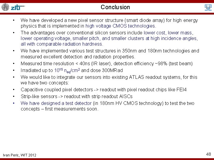
Conclusion • • • We have developed a new pixel sensor structure (smart diode array) for high energy physics that is implemented in high voltage CMOS technologies. The advantages over conventional silicon sensors include lower cost, lower mass, lower operating voltage, smaller pitch, and smaller clusters at high incidence angles, all with comparable radiation hardness. We have implemented various test structures in 350 nm and 180 nm technologies and measured excellent detection and radiation properties. Measured time resolution < 40 ns (IR laser), detection efficiency ~98% (test beam) Irradiated up to 1015 neq/cm 2 and dose 300 MRad We would like to integrate our sensors into existing ATLAS readout systems, for this we have two concepts: Capacitive coupled pixel detectors -> readout with pixel readout chips like FEI 4 Strip-like sensors -> readout with strip readout AISCs We have designed a test detector (in 180 nm HV CMOS technology) to test the two concepts – first measurements soon. Ivan Peric, WIT 2012 48

Thank you Ivan Peric, WIT 2012 49

Backup Slides Ivan Peric, WIT 2012 50

HV 2 FEI 4 - Architecture 12 x 2 Column control IO pads for strip operation Matrix Cap. Injection SFOut Test Pad 20 x 3 Column control Strip Pads Bias DACs IO pads for CCPD operation Ivan Peric, WIT 2012 51

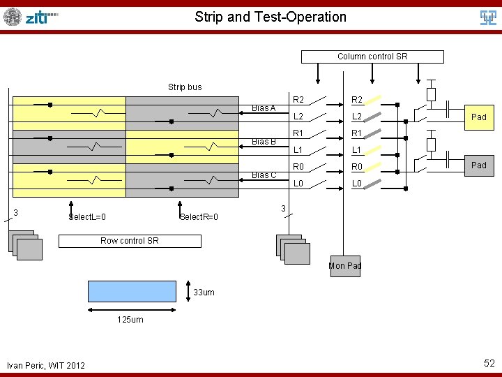
Strip and Test-Operation Column control SR Strip bus Bias A Bias B Bias C 3 Select. L=0 Select. R=0 R 2 L 2 R 1 L 1 R 0 L 0 Pad 3 Row control SR Mon Pad 33 um 125 um Ivan Peric, WIT 2012 52

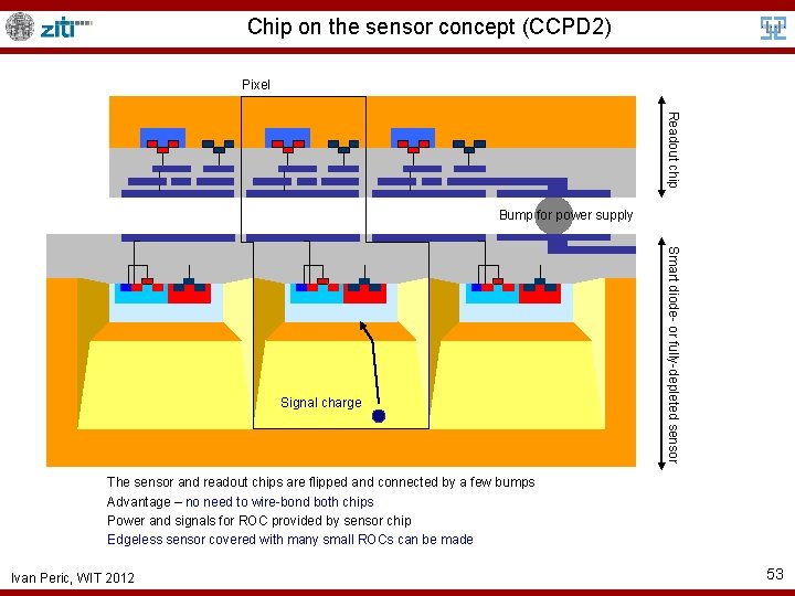
Chip on the sensor concept (CCPD 2) Pixel Readout chip Bump for power supply Smart diode- or fully-depleted sensor Signal charge The sensor and readout chips are flipped and connected by a few bumps Advantage – no need to wire-bond both chips Power and signals for ROC provided by sensor chip Edgeless sensor covered with many small ROCs can be made Ivan Peric, WIT 2012 53

CCPD 2 – photographs of the chips CAPPIX Ivan Peric, WIT 2012 CAPSENSE Power and signal bumps 54

CCPD 2 detector - photograph Power supply and cont. signals for the readout chip 1. 5 mm Power supply and cont. signals for the sensor Readout chip (CAPPIX) Sensor chip (CAPSENSE) Ivan Peric, WIT 2012 55

Collection time measurement • Digital part To. T is proportional to collected charge Does not depend on collection speed Test signal Ampl. out del 1 1400 e Window Comp out Penetration depth of 850 nm light ~14 um? Similar distribution of charge generation as for MIPs? del 2 IR laser signal N-well 5 u m Ampl. out 1400 e Comp out 10 u m 60% drift Window 40% diffusion Ivan Peric, WIT 2012 56

Time walk measurement • Digital part Test signal Ampl. out Comp out del 1 Window Comp out Window del 2 Ivan Peric, WIT 2012 57