A Monolithic Pixel Detector in HighVoltage Technology Ivan

- Slides: 37

A Monolithic Pixel Detector in High-Voltage Technology Ivan Perić University of Mannheim This work draws on the results from an ongoing research project commissioned by the Landesstiftung Baden-Württemberg DPG Tagung 2003, Ivan Peric

Overview § Introduction to the high-voltage CMOS process § The idea behind the HV monolithic pixel Pixel electronics § Electrical tests - Noise - Threshold dispersion - Time over threshold § Measurements with radioactive sources - Estimation of the average MIP signal - Images § Outlook VERTEX 2006 2

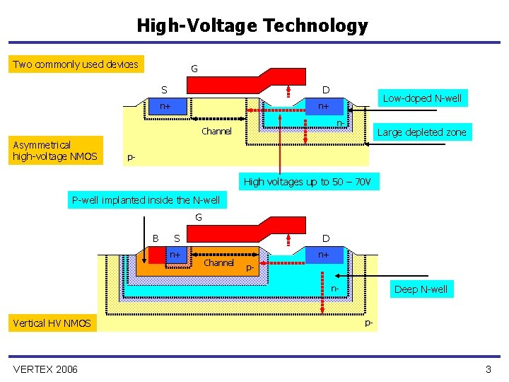
High-Voltage Technology Two commonly used devices G S D n+ n+ n- Channel Asymmetrical high-voltage NMOS Low-doped N-well Large depleted zone p- High voltages up to 50 – 70 V P-well implanted inside the N-well G B S n+ D Channel n+ p- Deep N-well n- Vertical HV NMOS VERTEX 2006 p- 3

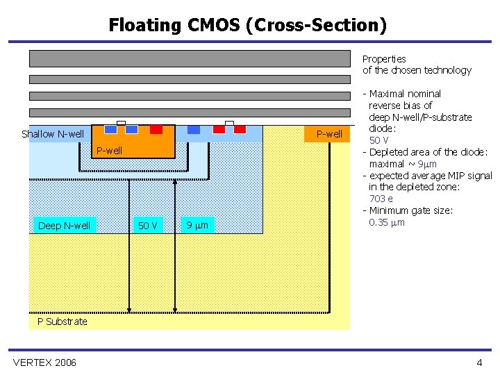
Floating CMOS (Cross-Section) Properties of the chosen technology Shallow N-well P-well Deep N-well 50 V 9 m - Maximal nominal reverse bias of deep N-well/P-substrate diode: 50 V - Depleted area of the diode: maximal ~ 9 m - expected average MIP signal in the depleted zone: 703 e - Minimum gate size: 0. 35 m P Substrate VERTEX 2006 4

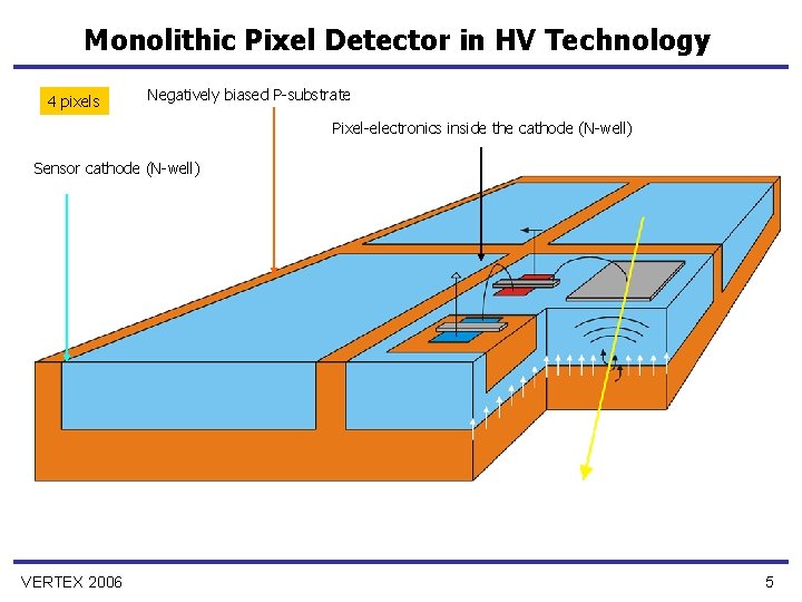
Monolithic Pixel Detector in HV Technology 4 pixels Negatively biased P-substrate Pixel-electronics inside the cathode (N-well) Sensor cathode (N-well) VERTEX 2006 5

Test Chip The first test-chip have been implemented in a 0. 35 m HV CMOS Process Motivations - to investigate the properties of deep N-well/P-substrate diode as a particle sensor - to demonstrate that it is possible to implement complex CMOS pixel electronic in the diode cathode (The electronics can involve - signal amplification, - continuous bias/reset, - threshold discrimination, - hit bit storage - time stamp electronic ) VERTEX 2006 6

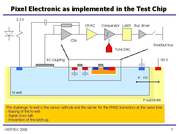
Pixel Electronic as implemented in the Test Chip 3. 3 V CR-RC Comparator Latch Bus driver CSA Readout bus Tune DAC AC coupling -50 V HV N-well P-substrate The challenge: N-well is the sensor cathode and the carrier for the PMOS transistors at the same time - Biasing of the N-well - Signal cross-talk - Prevention of the latch-up VERTEX 2006 7

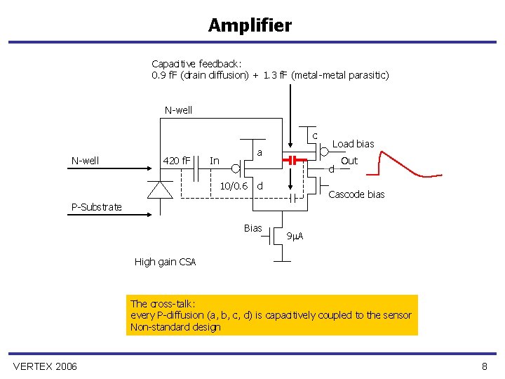
Amplifier Capacitive feedback: 0. 9 f. F (drain diffusion) + 1. 3 f. F (metal-metal parasitic) N-well c N-well 420 f. F In a Load bias d 10/0. 6 d Out Cascode bias P-Substrate Bias 9 A High gain CSA The cross-talk: every P-diffusion (a, b, c, d) is capacitively coupled to the sensor Non-standard design VERTEX 2006 8

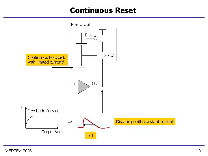
Continuous Reset Bias circuit Bias 30 p. A Continuous feedback with limited current* In * Out Feedback Current Output Volt. VERTEX 2006 Discharge with constant current To. T 9

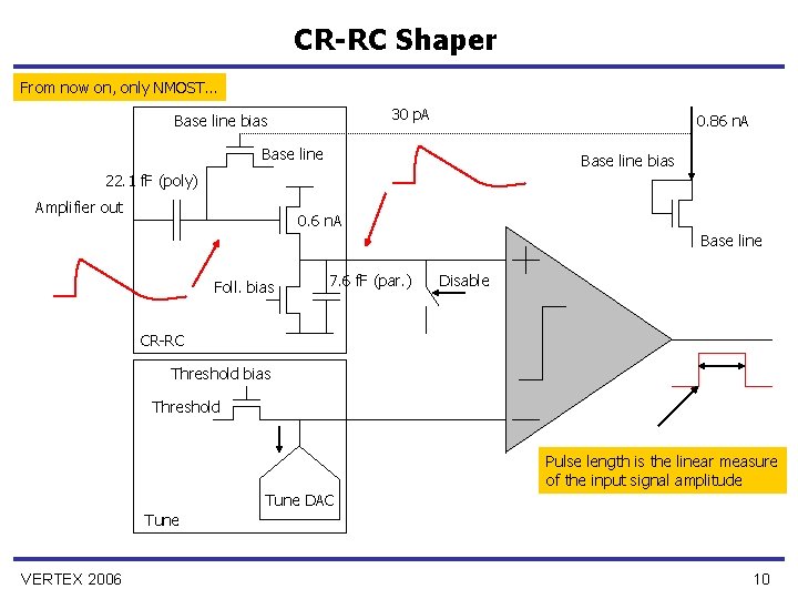
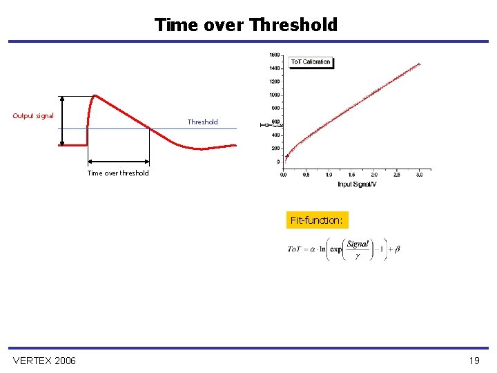
CR-RC Shaper From now on, only NMOST… 30 p. A Base line bias 0. 86 n. A Base line bias 22. 1 f. F (poly) Amplifier out 0. 6 n. A Base line Foll. bias 7. 6 f. F (par. ) Disable CR-RC Threshold bias Threshold Pulse length is the linear measure of the input signal amplitude Tune DAC Tune VERTEX 2006 10

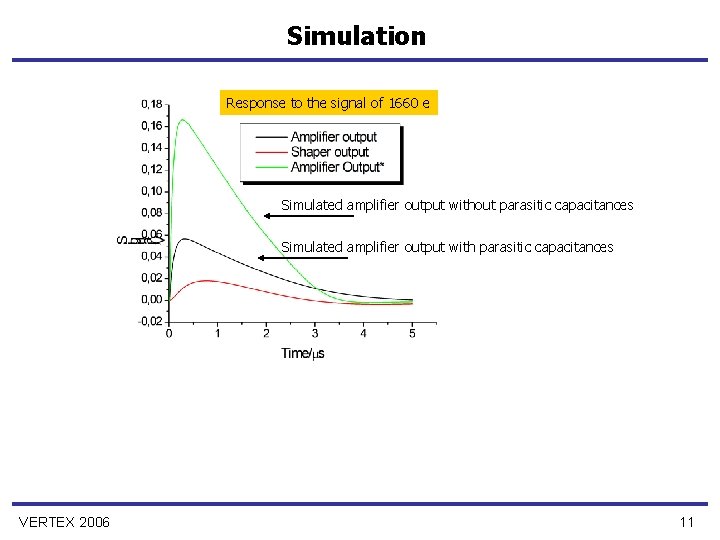
Simulation Response to the signal of 1660 e Simulated amplifier output without parasitic capacitances Simulated amplifier output with parasitic capacitances VERTEX 2006 11

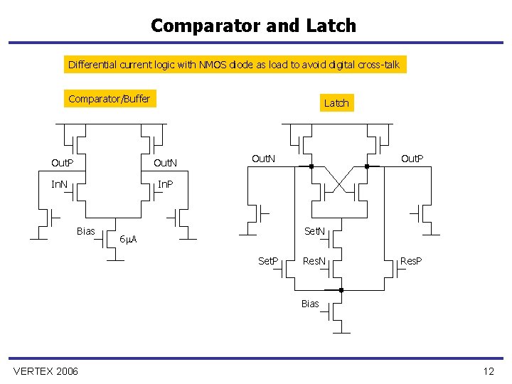
Comparator and Latch Differential current logic with NMOS diode as load to avoid digital cross-talk Comparator/Buffer Latch Out. P Out. N In. P Bias Out. N Out. P Set. N 6 A Set. P Res. N Res. P Bias VERTEX 2006 12

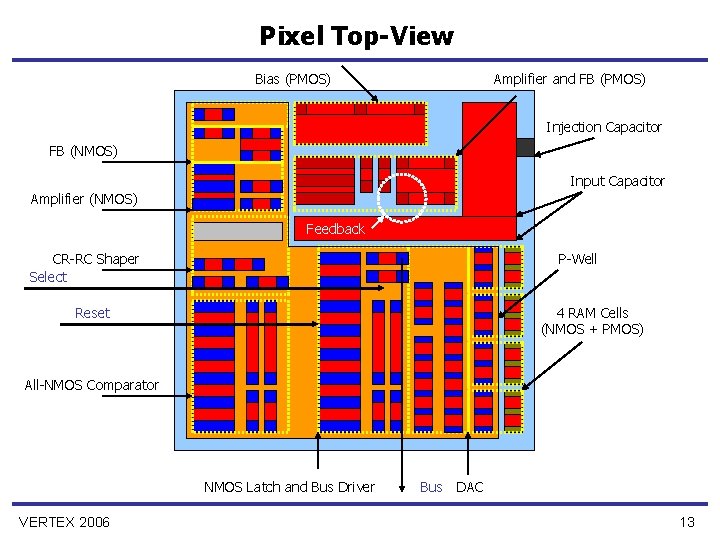
Pixel Top-View Bias (PMOS) Amplifier and FB (PMOS) Injection Capacitor FB (NMOS) Input Capacitor Amplifier (NMOS) Feedback CR-RC Shaper Select P-Well Reset 4 RAM Cells (NMOS + PMOS) All-NMOS Comparator NMOS Latch and Bus Driver VERTEX 2006 Bus DAC 13

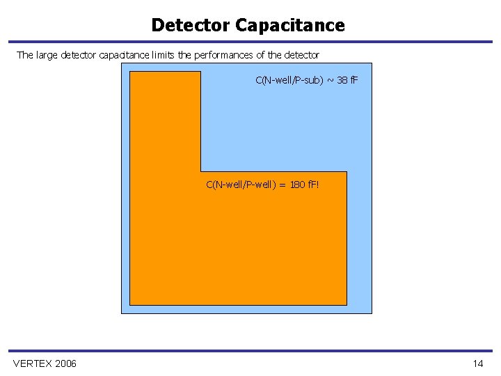
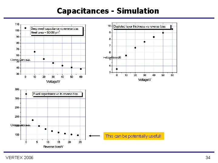
Detector Capacitance The large detector capacitance limits the performances of the detector C(N-well/P-sub) ~ 38 f. F C(N-well/P-well) = 180 f. F! VERTEX 2006 14

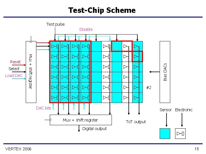
Test-Chip Scheme Test pulse Disable Load DAC Bias DACs Select Mux + shift register Reset #2 DAC bits Sensor Electronic Mux + shift register To. T output Digital output VERTEX 2006 15

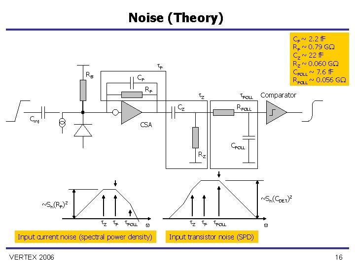
Noise (Theory) RB CF ~ 2. 2 f. F RF ~ 0. 79 G CZ ~ 22 f. F RZ ~ 0. 060 G CFOLL ~ 7. 6 f. F RFOLL ~ 0. 056 G F CF RF Z CZ Cinj FOLL Comparator RFOLL CSA RZ ~Sn(RF ~Sn(CDET)2 )2 Z F FOLL Input current noise (spectral power density) VERTEX 2006 CFOLL Z F FOLL Input transistor noise (SPD) 16

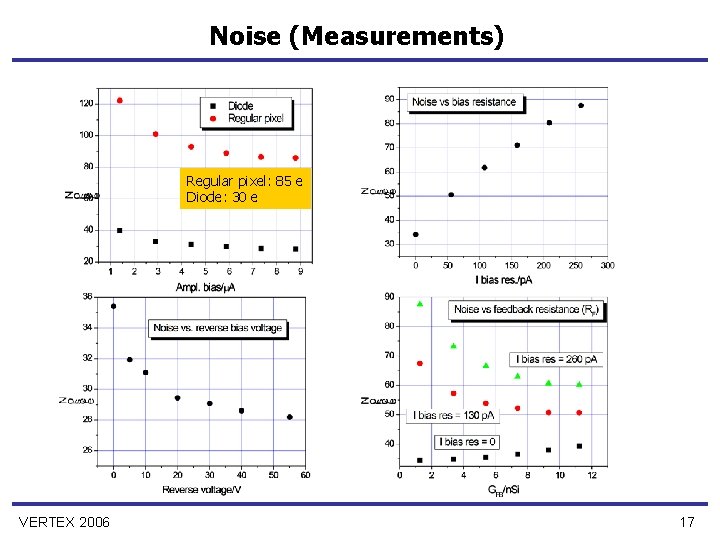
Noise (Measurements) Regular pixel: 85 e Diode: 30 e VERTEX 2006 17

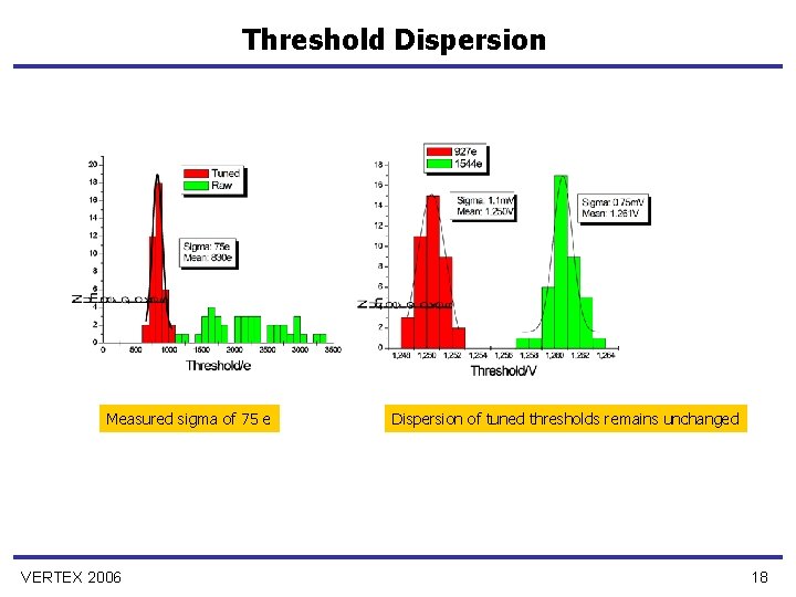
Threshold Dispersion Measured sigma of 75 e VERTEX 2006 Dispersion of tuned thresholds remains unchanged 18

Time over Threshold Output signal Threshold Time over threshold Fit-function: VERTEX 2006 19

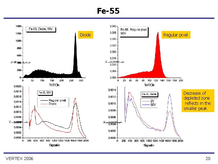
Fe-55 Diode Regular pixel Decrease of depleted zone reflects in the smaller peak VERTEX 2006 20

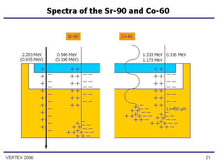
Spectra of the Sr-90 and Co-60 Sr-90 2. 283 Me. V (0. 935 Me. V) 0. 546 Me. V (0. 196 Me. V) Co-60 1. 333 Me. V 0. 316 Me. V 1. 173 Me. V L=450 m VERTEX 2006 21

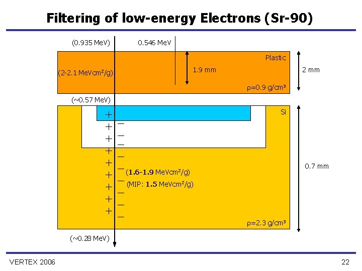
Filtering of low-energy Electrons (Sr-90) (0. 935 Me. V) 0. 546 Me. V Plastic 1. 9 mm (2 -2. 1 Me. Vcm 2/g) 2 mm =0. 9 g/cm 3 (~0. 57 Me. V) Si 0. 7 mm (1. 6 -1. 9 Me. Vcm 2/g) (MIP: 1. 5 Me. Vcm 2/g) =2. 3 g/cm 3 (~0. 28 Me. V) VERTEX 2006 22

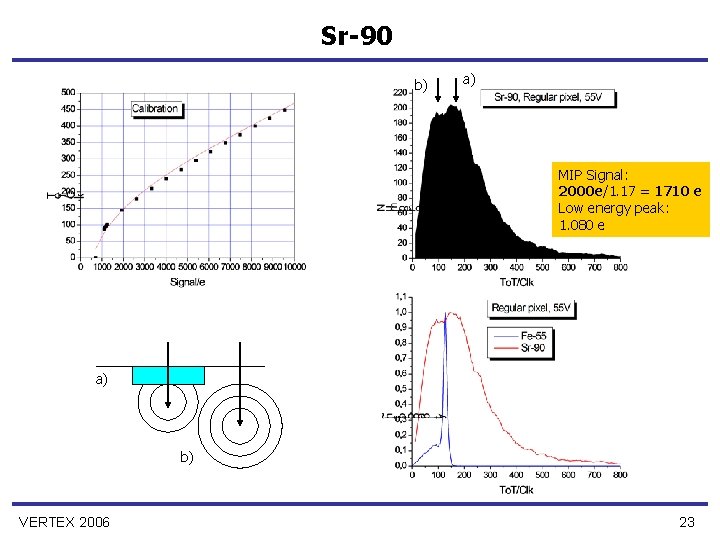
Sr-90 b) a) MIP Signal: 2000 e/1. 17 = 1710 e Low energy peak: 1. 080 e a) b) VERTEX 2006 23

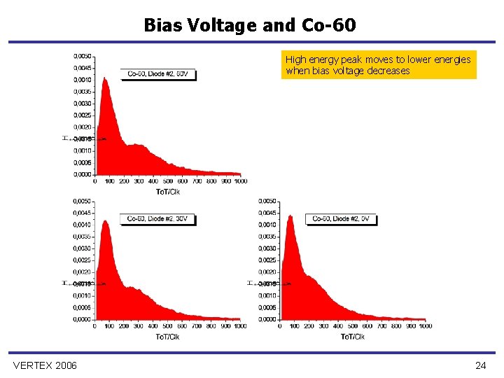
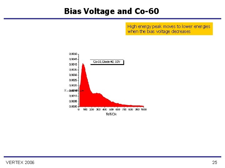
Bias Voltage and Co-60 High energy peak moves to lower energies when bias voltage decreases VERTEX 2006 24

Bias Voltage and Co-60 High energy peak moves to lower energies when the bias voltage decreases VERTEX 2006 25

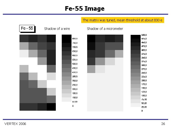
Fe-55 Image The matrix was tuned, mean threshold at about 830 e Shadow of a wire VERTEX 2006 Shadow of a micrometer 26

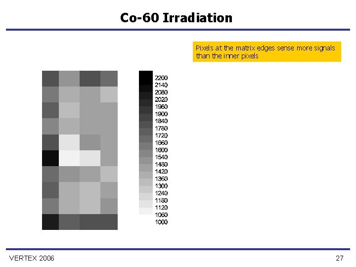
Co-60 Irradiation Pixels at the matrix edges sense more signals than the inner pixels VERTEX 2006 27

Summary § The idea: - The use of reverse biased N-well/P-substrate diode as sensor - Depleted zone of ~ 9 m can be induced by applying of relatively high bias voltage - CMOS pixel electronics can been implemented in the sensor cathode (N-well) § The first test-chip have been implemented in a 0. 35 m HV CMOS Process § The pixel electronics comprises - Charge sensitive amplifier and CR-RC shaper Continuous reset and bias Threshold discrimination with 4 -bit tune DAC NMOS-based latch and bus driver § Various electrical test demonstrate fully functionality of the detector § The average MIP signal estimated from the measurements with Sr-90 radioactive sources is 1710 e – it is by far more than expected; probably due to collection of the signal from bulk § Noise is about 80 e § Threshold dispersion is 75 e § Test-beam measurement has to be done; from the presented results I expect good efficiency of the detector § New submission with different test matrices is planned VERTEX 2006 28

Thank you for your attention VERTEX 2006 29

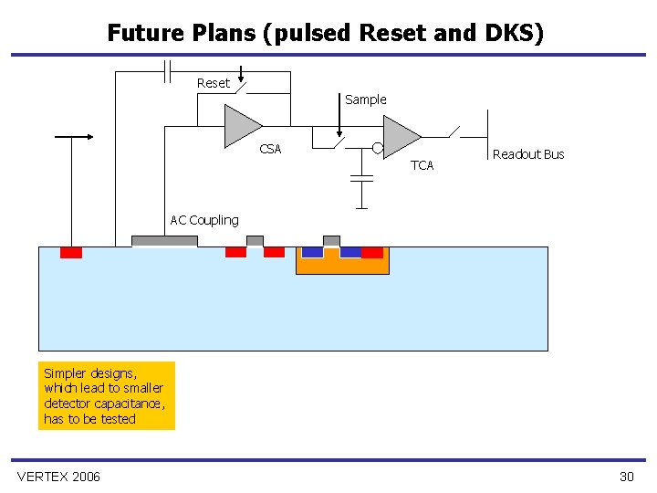
Future Plans (pulsed Reset and DKS) Reset Sample CSA TCA Readout Bus AC Coupling Simpler designs, which lead to smaller detector capacitance, has to be tested VERTEX 2006 30

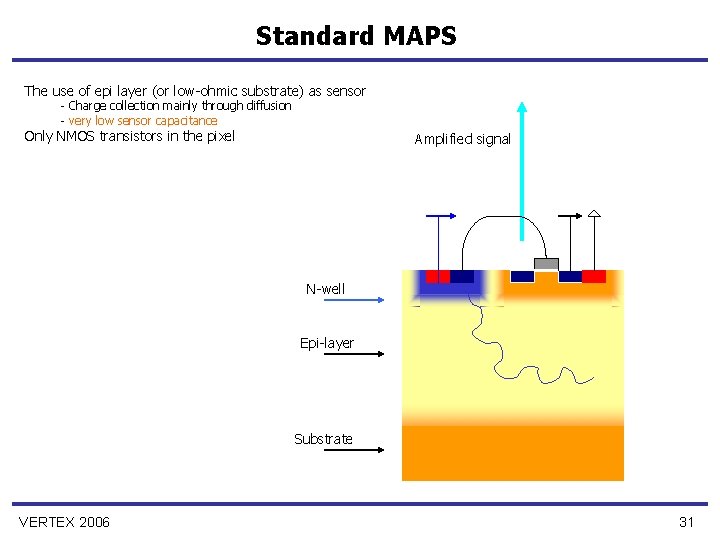
Standard MAPS The use of epi layer (or low-ohmic substrate) as sensor - Charge collection mainly through diffusion - very low sensor capacitance Only NMOS transistors in the pixel Amplified signal N-well Epi-layer Substrate VERTEX 2006 31

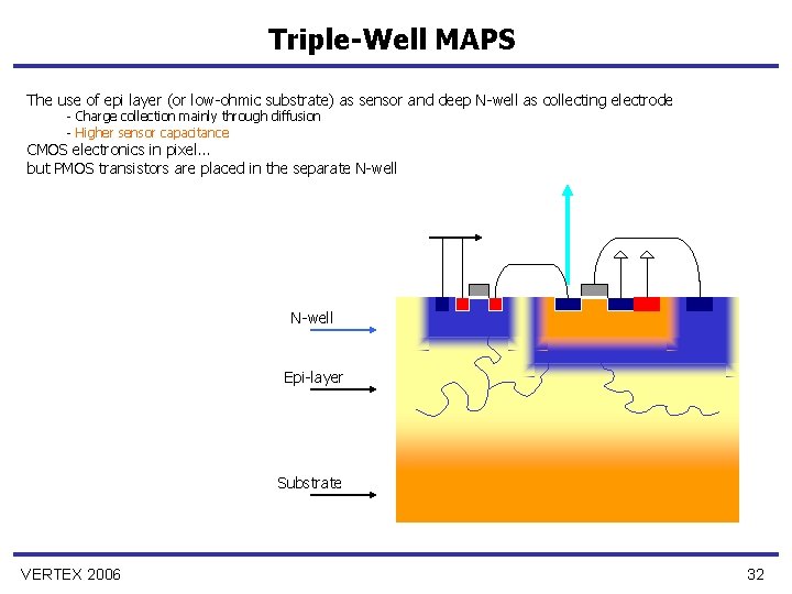
Triple-Well MAPS The use of epi layer (or low-ohmic substrate) as sensor and deep N-well as collecting electrode - Charge collection mainly through diffusion - Higher sensor capacitance CMOS electronics in pixel… but PMOS transistors are placed in the separate N-well Epi-layer Substrate VERTEX 2006 32

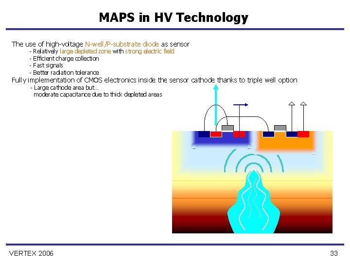
MAPS in HV Technology The use of high-voltage N-well/P-substrate diode as sensor - Relatively large depleted zone with strong electric field Efficient charge collection Fast signals Better radiation tolerance Fully implementation of CMOS electronics inside the sensor cathode thanks to triple well option - Large cathode area but… moderate capacitance due to thick depleted areas VERTEX 2006 33

Capacitances - Simulation This can be potentially useful! VERTEX 2006 34

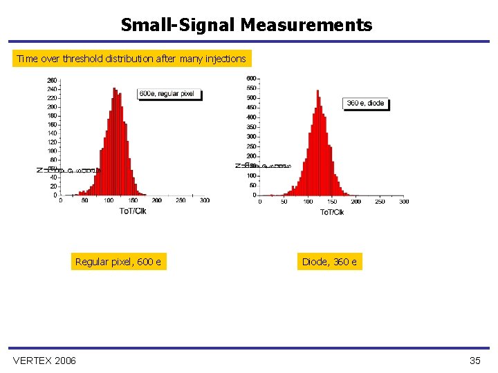
Small-Signal Measurements Time over threshold distribution after many injections Regular pixel, 600 e VERTEX 2006 Diode, 360 e 35

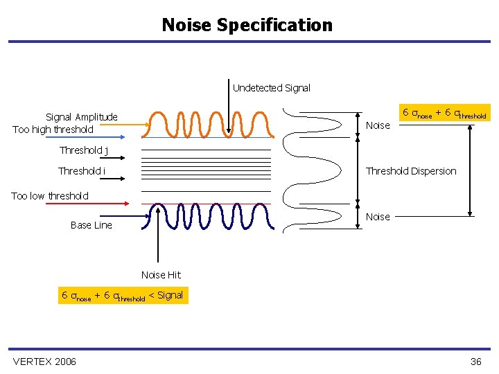
Noise Specification Undetected Signal Amplitude Too high threshold Noise 6 noise + 6 threshold Threshold j Threshold i Threshold Dispersion Too low threshold Noise Base Line Noise Hit 6 noise + 6 threshold < Signal VERTEX 2006 36

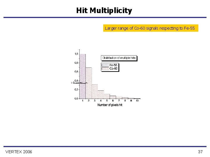
Hit Multiplicity Larger range of Co-60 signals respecting to Fe-55 VERTEX 2006 37