
Hybrid pixel pilot and bus K Tanida RIKEN
Hybrid pixel: pilot and bus K. Tanida (RIKEN) 06/09/03 Si upgrade workshop Outline • Overview on ALICE pilot and bus • Requirements • Pilot options • Bus options • R&D plans
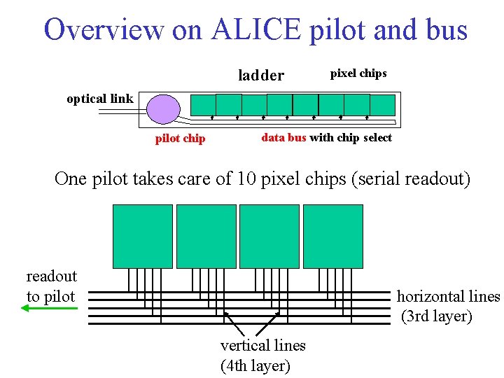
Overview on ALICE pilot and bus ladder pixel chips optical link pilot chip data bus with chip select One pilot takes care of 10 pixel chips (serial readout) readout to pilot horizontal lines (3 rd layer) vertical lines (4 th layer)

Bus: cross section 6 layers: Digital GND: Digital power: Hori. line: Vert. line: Analog power: Analog GND: 25 mm 10 mm 5 mm 25 mm passive components 290µm PIXELS DETECTOR 150 to 200µm READOUT CHIP carbon fiber support cooling • Material: Al (conductor) + Kapton (insulator) 150 to 200µm
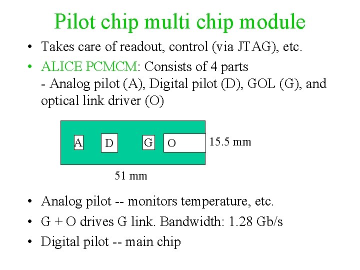
Pilot chip multi chip module • Takes care of readout, control (via JTAG), etc. • ALICE PCMCM: Consists of 4 parts - Analog pilot (A), Digital pilot (D), GOL (G), and optical link driver (O) A D G O 15. 5 mm 51 mm • Analog pilot -- monitors temperature, etc. • G + O drives G link. Bandwidth: 1. 28 Gb/s • Digital pilot -- main chip
Requirements • Parallel readout -- 8 chips max. - 256 lines instead of 32 Bus: high density and/or more layers Pilot: multi pilot chips or more inputs • Data size: 32× 256× 8 bit/event - 1. 6 Gb/s > 1. 28 Gb/s (ALICE G-link bandwidth) zero suppression at front-end • Other issues - Space (width: ~1. 5 cm) - thickness - cost, rate of bad product
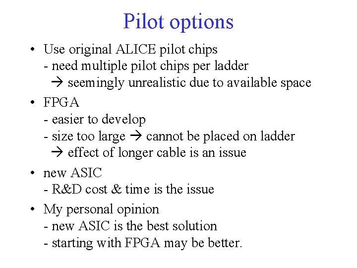
Pilot options • Use original ALICE pilot chips - need multiple pilot chips per ladder seemingly unrealistic due to available space • FPGA - easier to develop - size too large cannot be placed on ladder effect of longer cable is an issue • new ASIC - R&D cost & time is the issue • My personal opinion - new ASIC is the best solution - starting with FPGA may be better.
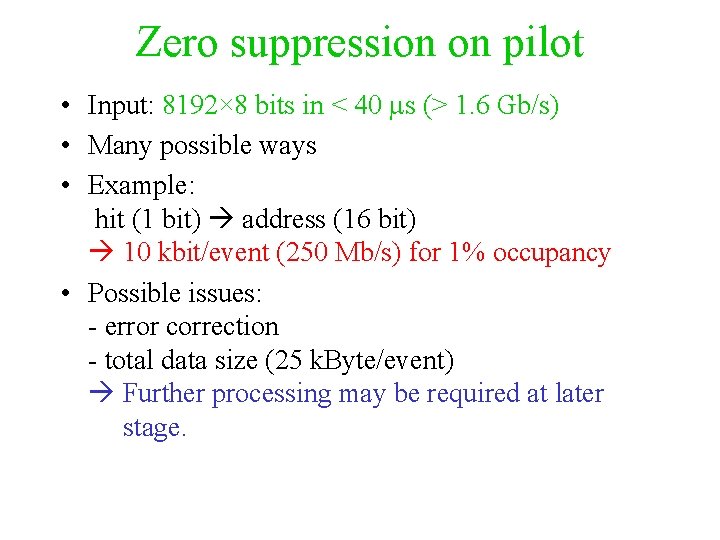
Zero suppression on pilot • Input: 8192× 8 bits in < 40 ms (> 1. 6 Gb/s) • Many possible ways • Example: hit (1 bit) address (16 bit) 10 kbit/event (250 Mb/s) for 1% occupancy • Possible issues: - error correction - total data size (25 k. Byte/event) Further processing may be required at later stage.
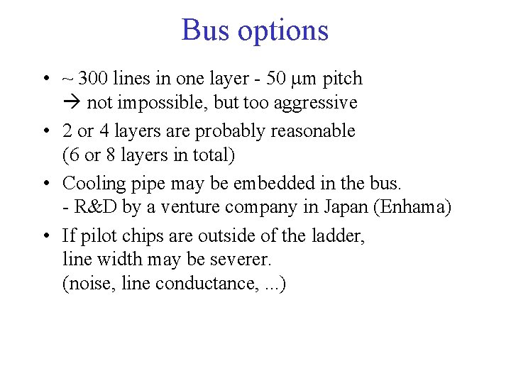
Bus options • ~ 300 lines in one layer - 50 mm pitch not impossible, but too aggressive • 2 or 4 layers are probably reasonable (6 or 8 layers in total) • Cooling pipe may be embedded in the bus. - R&D by a venture company in Japan (Enhama) • If pilot chips are outside of the ladder, line width may be severer. (noise, line conductance, . . . )
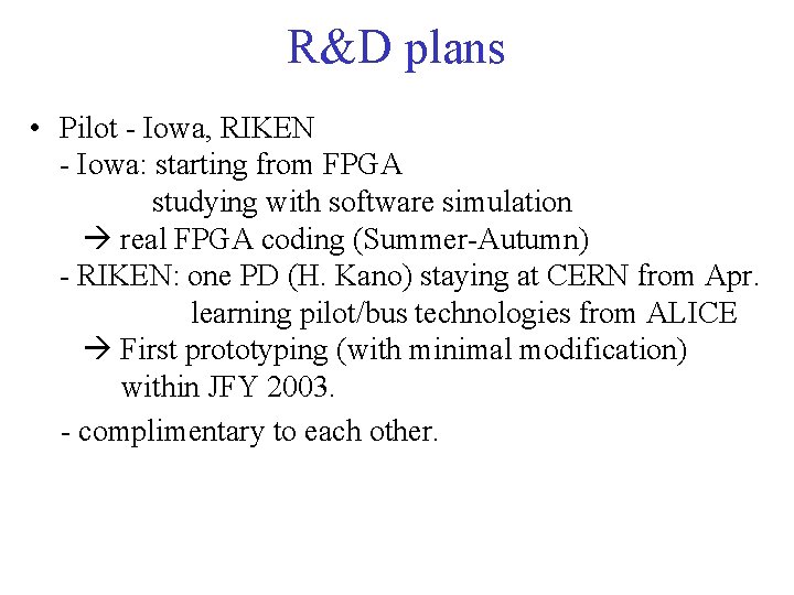
R&D plans • Pilot - Iowa, RIKEN - Iowa: starting from FPGA studying with software simulation real FPGA coding (Summer-Autumn) - RIKEN: one PD (H. Kano) staying at CERN from Apr. learning pilot/bus technologies from ALICE First prototyping (with minimal modification) within JFY 2003. - complimentary to each other.
Bus R&D • First trial on prototyping with minimal modification - same bus configuration - PCMCM and bus are on the same (flexy) board - power, GND: Al, signal lines: Cu - try cooling pipe embedded bus • Currently doing design with KEK engineers. Submit by July, expecting to finish in Autumn. • If successful, we will try buses with more layers/lines-per-layer.
Summary • Pilot chip/bus modification is required due to readout time limit in PHENIX. • Up to 8 chips must be read out in parallel. Zero suppression at pilot is also necessary. • Pilot R&D: Iowa (FPGA) and RIKEN (ASIC) - complimentary to each other. • Bus R&D: RIKEN • Both started. First prototype will be available in this year.
- Slides: 11