Overview of HVHRCMOS Pixel Sensors Ivan Peric PIXEL








- Slides: 83

Overview of HV/HR-CMOS Pixel Sensors Ivan Peric PIXEL 2014, Niagara Falls, Canada 1

HVCMOS Introduction PIXEL 2014, Niagara Falls, Canada 2

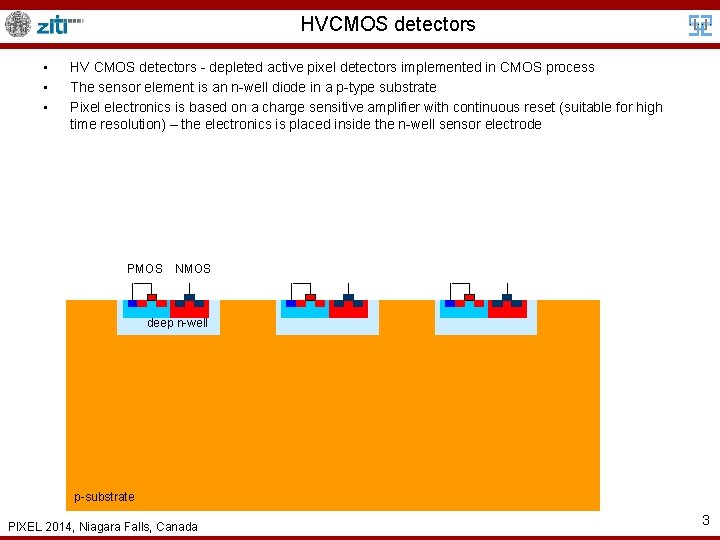
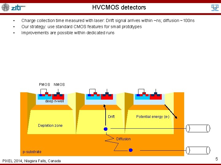
HVCMOS detectors • • • HV CMOS detectors - depleted active pixel detectors implemented in CMOS process The sensor element is an n-well diode in a p-type substrate Pixel electronics is based on a charge sensitive amplifier with continuous reset (suitable for high time resolution) – the electronics is placed inside the n-well sensor electrode PMOS NMOS deep n-well p-substrate PIXEL 2014, Niagara Falls, Canada 3

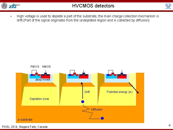
HVCMOS detectors • High voltage is used to deplete a part of the substrate, the main charge collection mechanism is drift (Part of the signal originates from the undepleted region and is collected by diffusion) PMOS NMOS deep n-well Drift Potential energy (e-) Depletion zone Diffusion p-substrate PIXEL 2014, Niagara Falls, Canada 4

HVCMOS detectors • • • Charge collection time measured with laser: Drift signal arrives within ~ns; diffusion ~100 ns Our strategy: use standard CMOS features for small prototypes Improvements are possible within dedicated runs PMOS NMOS deep n-well Drift Potential energy (e-) Depletion zone Diffusion p-substrate PIXEL 2014, Niagara Falls, Canada 5

Improved HVCMOS Structures HRCMOS PIXEL 2014, Niagara Falls, Canada 6

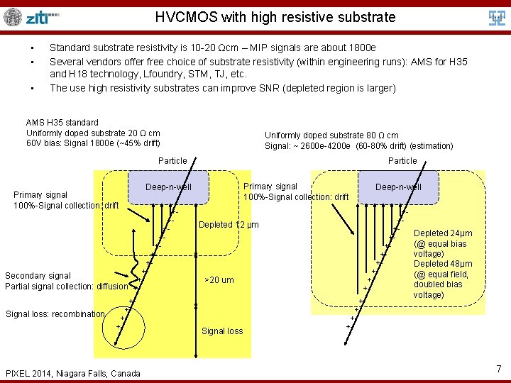
HVCMOS with high resistive substrate • • • Standard substrate resistivity is 10 -20 Ωcm – MIP signals are about 1800 e Several vendors offer free choice of substrate resistivity (within engineering runs): AMS for H 35 and H 18 technology, Lfoundry, STM, TJ, etc. The use high resistivity substrates can improve SNR (depleted region is larger) AMS H 35 standard Uniformly doped substrate 20 Ω cm 60 V bias: Signal 1800 e (~45% drift) Uniformly doped substrate 80 Ω cm Signal: ~ 2600 e-4200 e (60 -80% drift) (estimation) Particle Primary signal 100%-Signal collection: drift Deep-n-well ++++Secondary signal +Partial signal collection: diffusion +++Signal loss: recombination ++- PIXEL 2014, Niagara Falls, Canada Particle Depleted 12 µm >20 um Signal loss Deep-n-well +++++++- Depleted 24µm (@ equal bias voltage) Depleted 48µm (@ equal field, doubled bias voltage) 7

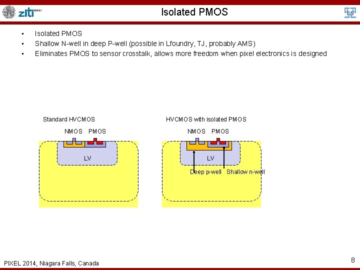
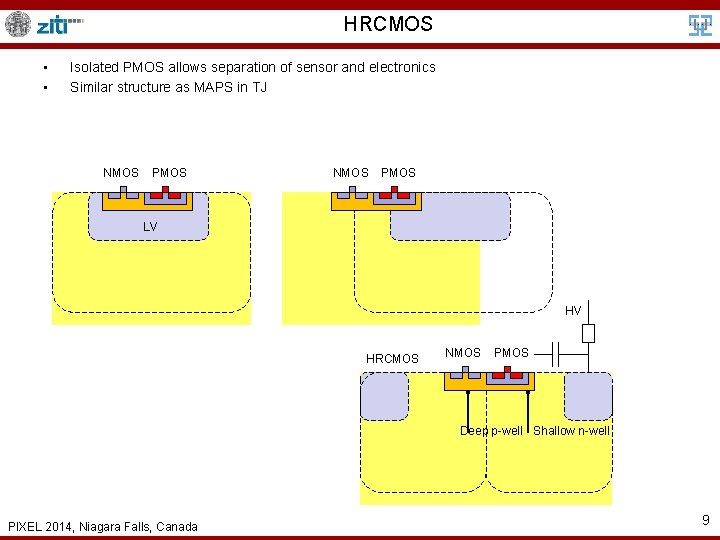
Isolated PMOS • • • Isolated PMOS Shallow N-well in deep P-well (possible in Lfoundry, TJ, probably AMS) Eliminates PMOS to sensor crosstalk, allows more freedom when pixel electronics is designed Standard HVCMOS NMOS PMOS LV HVCMOS with isolated PMOS NMOS PMOS LV Deep p-well Shallow n-well PIXEL 2014, Niagara Falls, Canada 8

HRCMOS • • Isolated PMOS allows separation of sensor and electronics Similar structure as MAPS in TJ NMOS PMOS LV HV HRCMOS NMOS PMOS Deep p-well Shallow n-well PIXEL 2014, Niagara Falls, Canada 9

HVCMOS Projects PIXEL 2014, Niagara Falls, Canada 10

Mu 3 e PIXEL 2014, Niagara Falls, Canada 11

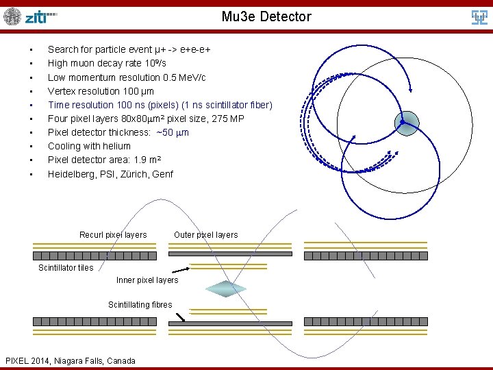
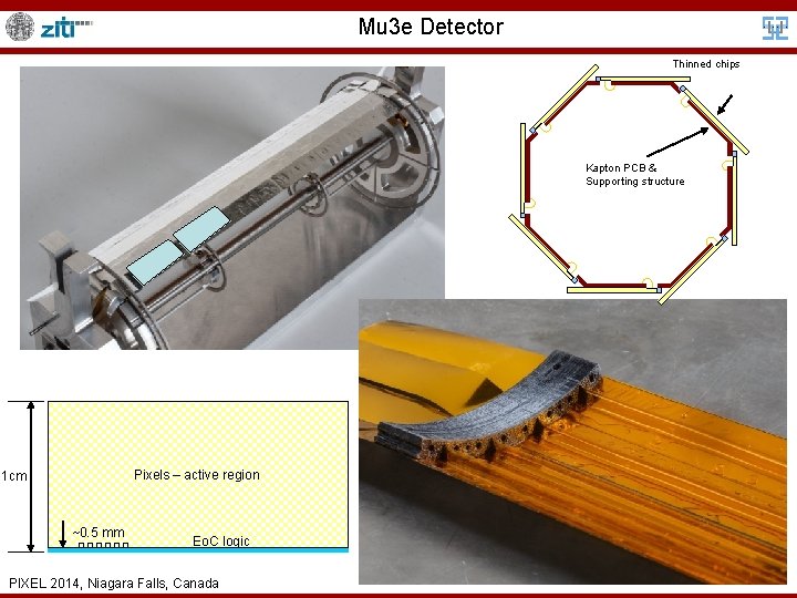
Mu 3 e Detector • • • Search for particle event µ+ -> e+e-e+ High muon decay rate 109/s Low momentum resolution 0. 5 Me. V/c Vertex resolution 100 µm Time resolution 100 ns (pixels) (1 ns scintillator fiber) Four pixel layers 80 x 80 m 2 pixel size, 275 MP Pixel detector thickness: ~50 m Cooling with helium Pixel detector area: 1. 9 m 2 Heidelberg, PSI, Zürich, Genf Recurl pixel layers Outer pixel layers Scintillator tiles Inner pixel layers Scintillating fibres PIXEL 2014, Niagara Falls, Canada

Mu 3 e Detector Thinned chips Kapton PCB & Supporting structure Pixels – active region 1 cm ~0. 5 mm Eo. C logic PIXEL 2014, Niagara Falls, Canada

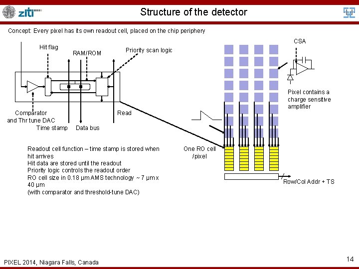
Structure of the detector Concept: Every pixel has its own readout cell, placed on the chip periphery Hit flag Comparator and Thr tune DAC Time stamp CSA RAM/ROM Priority scan logic Pixel contains a charge sensitive amplifier Read Data bus Readout cell function – time stamp is stored when hit arrives Hit data are stored until the readout Priority logic controls the readout order RO cell size in 0. 18 µm AMS technology ~ 7 µm x 40 µm (with comparator and threshold-tune DAC) PIXEL 2014, Niagara Falls, Canada One RO cell /pixel Row/Col Addr + TS 14

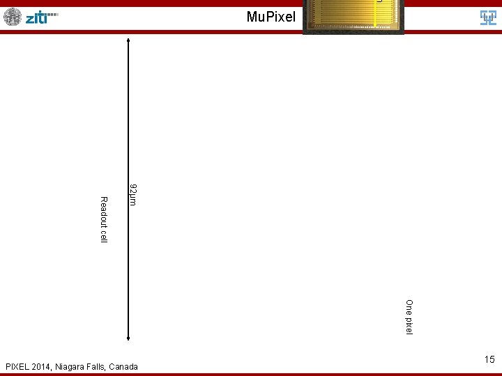
m Mu. Pixel 92µm Readout cell One pixel PIXEL 2014, Niagara Falls, Canada 15

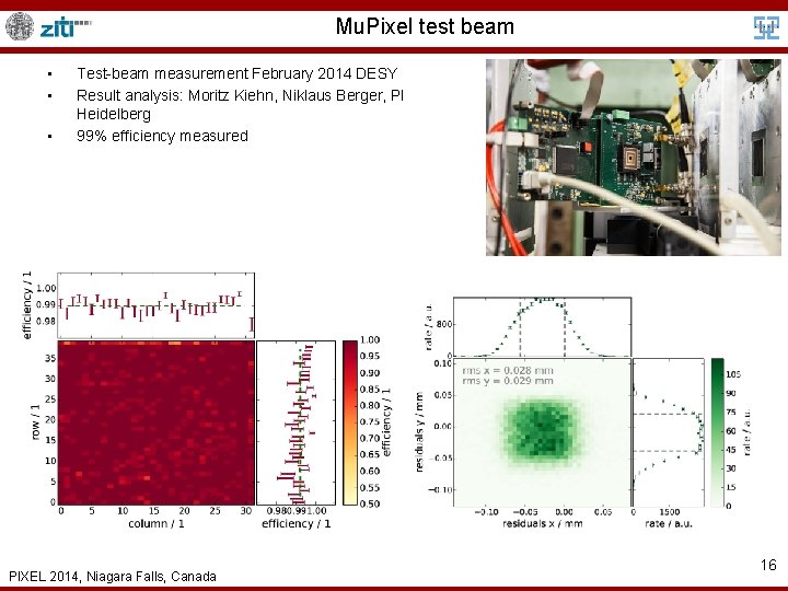
Mu. Pixel test beam • • • Test-beam measurement February 2014 DESY Result analysis: Moritz Kiehn, Niklaus Berger, PI Heidelberg 99% efficiency measured PIXEL 2014, Niagara Falls, Canada 16

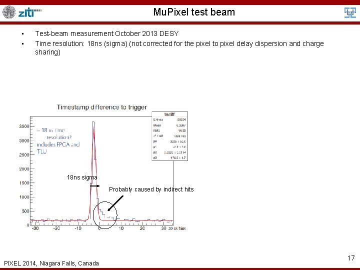
Mu. Pixel test beam • • Test-beam measurement October 2013 DESY Time resolution: 18 ns (sigma) (not corrected for the pixel to pixel delay dispersion and charge sharing) 18 ns sigma Probably caused by indirect hits PIXEL 2014, Niagara Falls, Canada 17

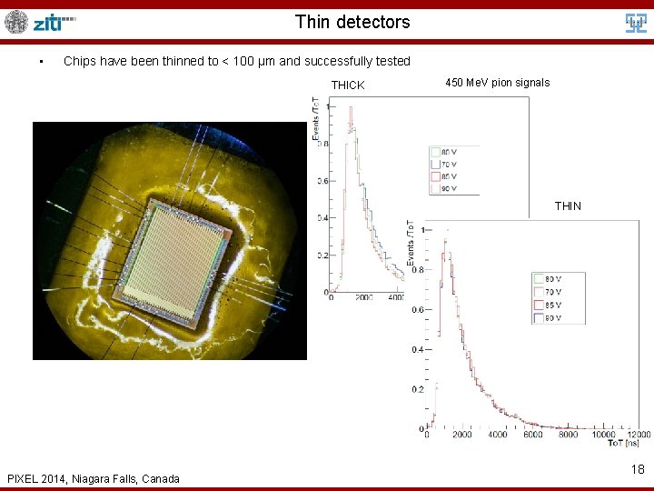
Thin detectors • Chips have been thinned to < 100 μm and successfully tested THICK 450 Me. V pion signals THIN PIXEL 2014, Niagara Falls, Canada 18

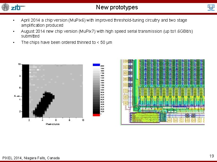
New prototypes • • • April 2014 a chip version (Mu. Pix 6) with improved threshold-tuning circuitry and two stage amplification produced August 2014 new chip version (Mu. Pix 7) with high speed serial transmission (up to 1. 6 GBit/s) submitted The chips have been ordered thinned to < 50 μm PIXEL 2014, Niagara Falls, Canada 19

ATLAS Pixels CPPM Marseille, CERN, University of Geneve, INFN Genova, Bonn University, LBNL Berkeley, University of Göttingen, Jozef Stefan Institute Ljubljana, University of Glasgow, University of Liverpool, IFAE Barcelona, Heidelberg University… PIXEL 2014, Niagara Falls, Canada 20

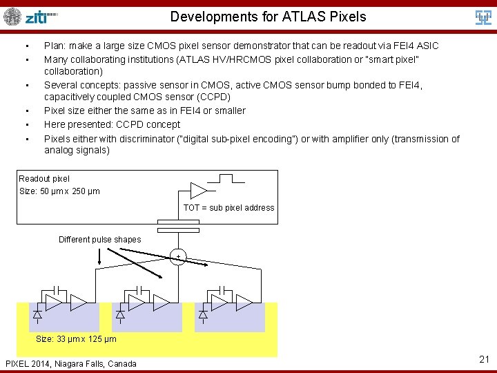
Developments for ATLAS Pixels • • • Plan: make a large size CMOS pixel sensor demonstrator that can be readout via FEI 4 ASIC Many collaborating institutions (ATLAS HV/HRCMOS pixel collaboration or “smart pixel” collaboration) Several concepts: passive sensor in CMOS, active CMOS sensor bump bonded to FEI 4, capacitively coupled CMOS sensor (CCPD) Pixel size either the same as in FEI 4 or smaller Here presented: CCPD concept Pixels either with discriminator (“digital sub-pixel encoding”) or with amplifier only (transmission of analog signals) Readout pixel Size: 50 µm x 250 µm TOT = sub pixel address Different pulse shapes + Size: 33 µm x 125 µm PIXEL 2014, Niagara Falls, Canada 21

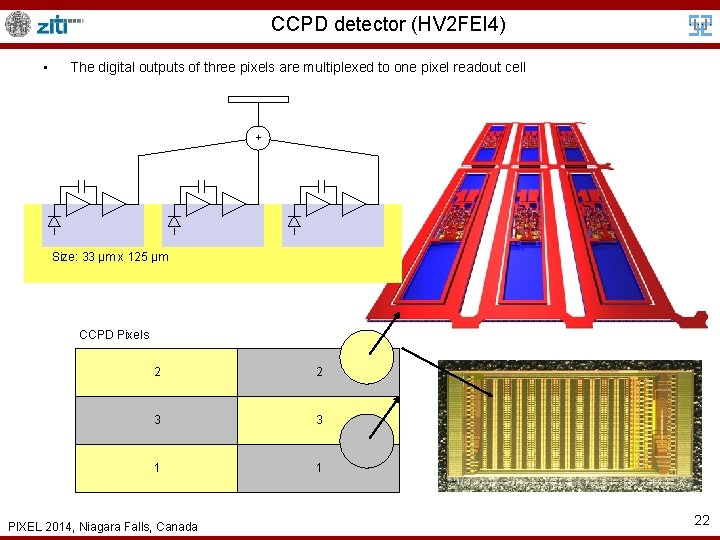
CCPD detector (HV 2 FEI 4) • The digital outputs of three pixels are multiplexed to one pixel readout cell + Size: 33 µm x 125 µm CCPD Pixels 2 2 3 3 1 1 PIXEL 2014, Niagara Falls, Canada 22

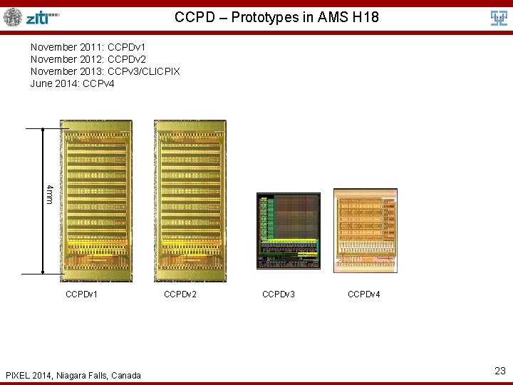
CCPD – Prototypes in AMS H 18 November 2011: CCPDv 1 November 2012: CCPDv 2 November 2013: CCPv 3/CLICPIX June 2014: CCPv 4 4 mm CCPDv 1 PIXEL 2014, Niagara Falls, Canada CCPDv 2 CCPDv 3 CCPDv 4 23

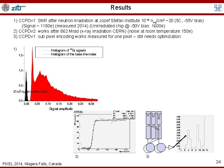
Results 1) CCPDv 1: SNR after neutron irradiation at Jozef Stefan Institute 1015 neq/cm 2 ~20 (5 C, -55 V bias) (Signal ~ 1180 e) (measured 2014) (Unirradiated chip @ -50 V bias: 1600 e) 2) CCPDv 2: works after 862 Mrad (x-ray irradiation CERN) (noise at room temperature 150 e) 3) CCPDv 1: sub pixel encoding works measured for one pixel – still needs optimization 1) 2) PIXEL 2014, Niagara Falls, Canada 3) 24

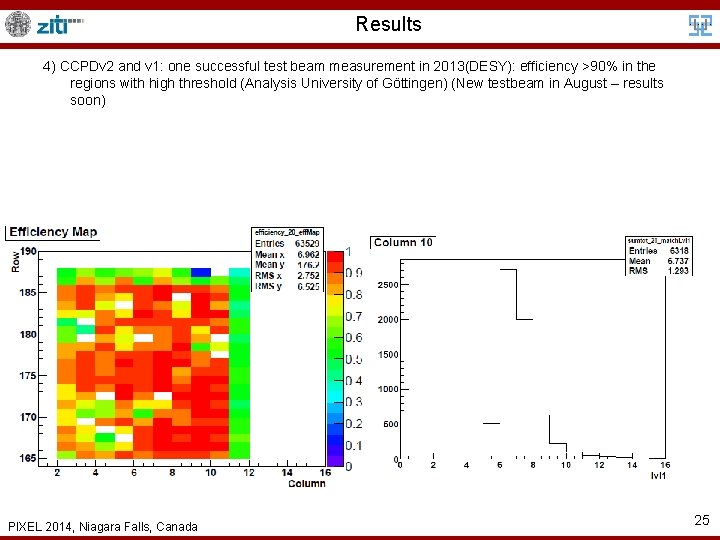
Results 4) CCPDv 2 and v 1: one successful test beam measurement in 2013(DESY): efficiency >90% in the regions with high threshold (Analysis University of Göttingen) (New testbeam in August – results soon) 2) PIXEL 2014, Niagara Falls, Canada 25

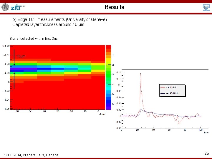
Results 5) Edge TCT measurements (University of Geneve) Depleted layer thickness around 15 μm Signal collected within first 3 ns 15μm PIXEL 2014, Niagara Falls, Canada 26

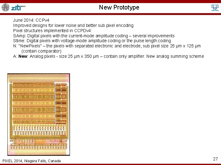
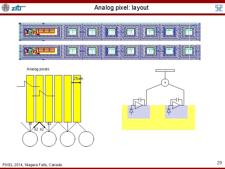
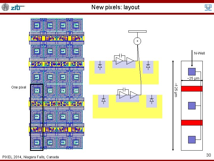
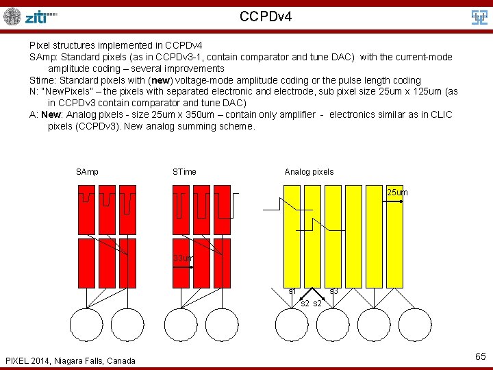
New Prototype June 2014: CCPv 4 Improved designs for lower noise and better sub pixel encoding Pixel structures implemented in CCPDv 4: SAmp: Digital pixels with the current-mode amplitude coding – several improvements Stime: Digital pixels with voltage-mode amplitude coding or the pulse length coding N: “New. Pixels” – the pixels with separated electronic and electrode, sub pixel size 25 μm x 125 μm (contain comparator) A: New: Analog pixels - size 25 μm x 350 μm – contain only amplifier. New analog summing scheme PIXEL 2014, Niagara Falls, Canada 27

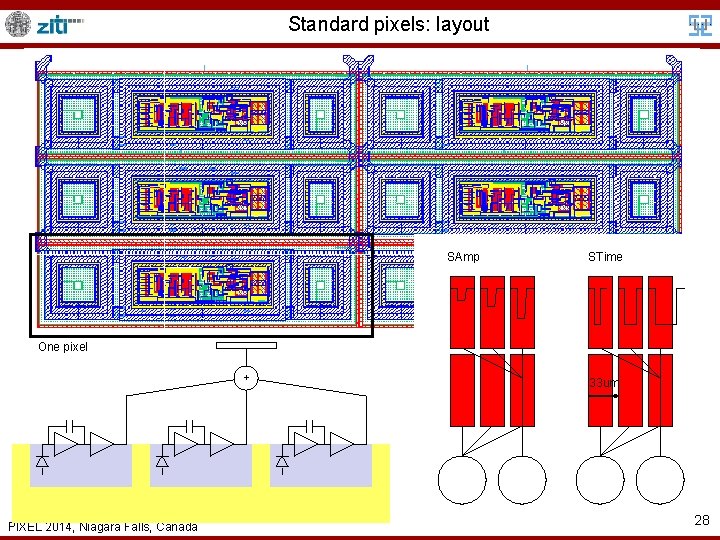
Standard pixels: layout SAmp STime One pixel + PIXEL 2014, Niagara Falls, Canada 33 um 28

Analog pixel: layout Analog pixels 25 um s 1 + s 3 s 2 PIXEL 2014, Niagara Falls, Canada 29

New pixels: layout + N-Well ~25 µm PIXEL 2014, Niagara Falls, Canada ~125 µm One pixel 30

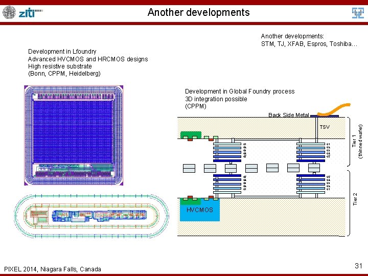
Another developments: STM, TJ, XFAB, Espros, Toshiba… Development in Lfoundry Advanced HVCMOS and HRCMOS designs High resistive substrate (Bonn, CPPM, Heidelberg) Development in Global Foundry process 3 D integration possible (CPPM) TSV M 1 M 2 M 3 M 4 M 5 M 4 M 3 M 2 M 1 Tier 2 M 1 M 2 M 3 M 4 M 5 Tier 1 (thinned wafer) Back Side Metal HVCMOS PIXEL 2014, Niagara Falls, Canada 31

CLIC PIXEL 2014, Niagara Falls, Canada 32

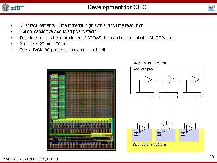
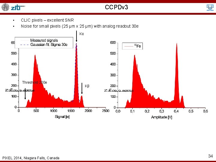
Development for CLIC • • • CLIC requirements – little material, high spatial and time resolution Option: capacitively coupled pixel detector Test detector has been produced (CCPDv 3) that can be readout with CLICPIX chip Pixel size: 25 µm x 25 µm Every HVCMOS pixel has its own readout cell Size: 25 µm x 25 µm Readout pixel Size: 25 µm x 25 µm PIXEL 2014, Niagara Falls, Canada 33

CCPDv 3 • • CLIC pixels – excellent SNR Noise for small pixels (25 μm x 25 μm) with analog readout 30 e Kα Threshold 200 e PIXEL 2014, Niagara Falls, Canada Kβ 34

ATLAS Strips PIXEL 2014, Niagara Falls, Canada 35

HVCMOS for ATLAS strip layers The development is coordinated by ATLAS strip WP 1 Presently two CMOS technologies are investigated: AMS H 35 and TJ (LF development is planned) Heidelberg: AMS (and LF) The foundries offer inexpensive engineering runs with high resistive substrates and low cost production PIXEL 2014, Niagara Falls, Canada 36

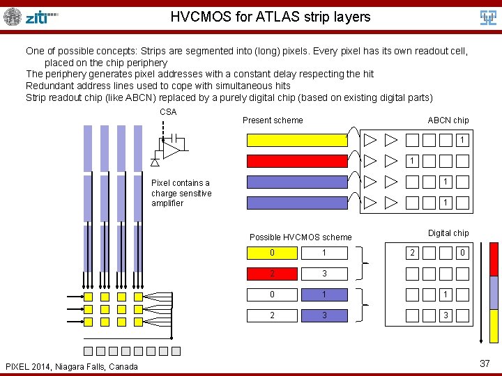
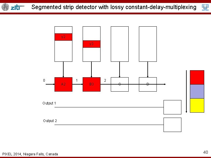
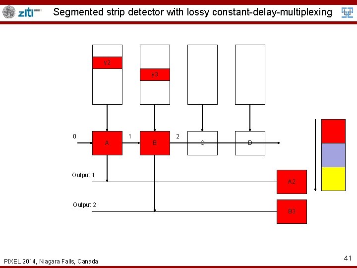
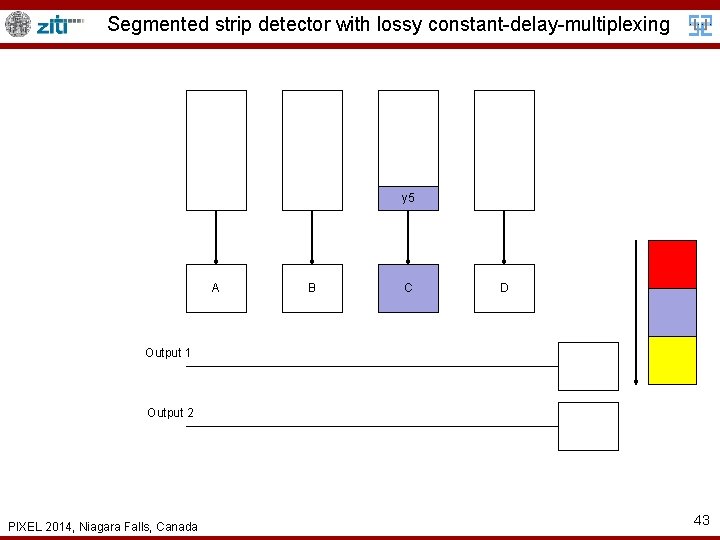
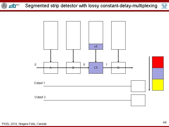
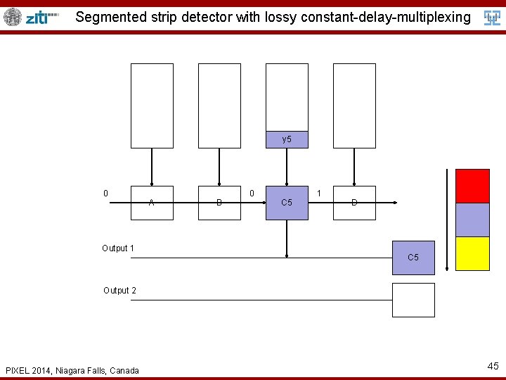
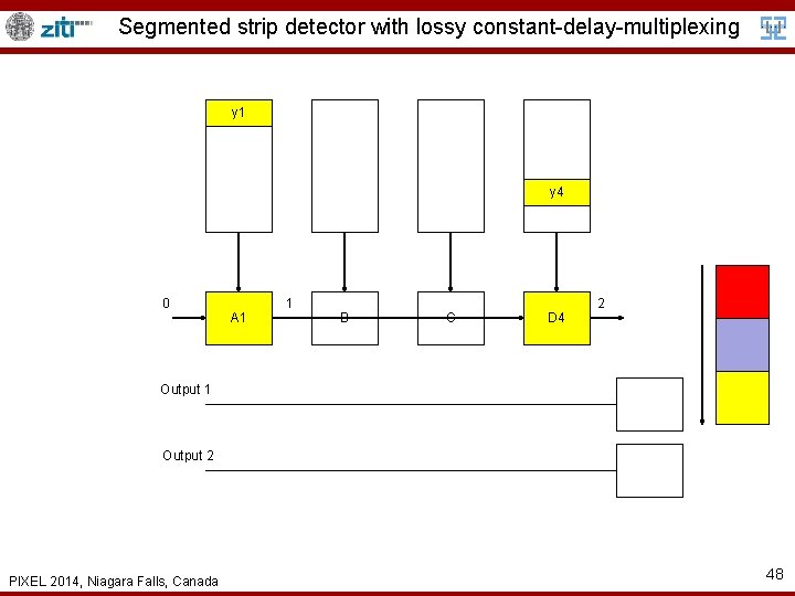
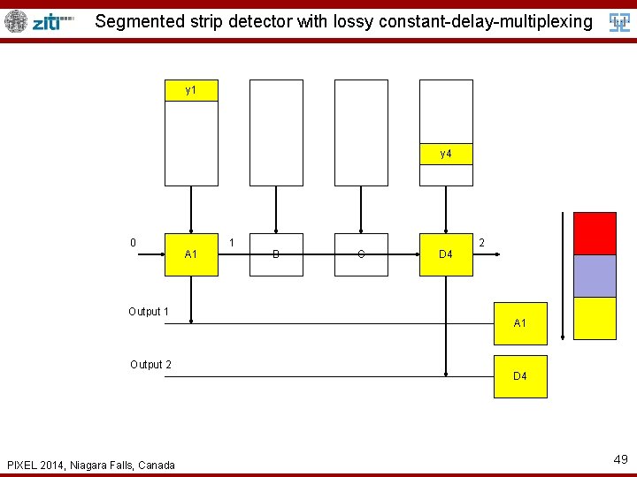
HVCMOS for ATLAS strip layers One of possible concepts: Strips are segmented into (long) pixels. Every pixel has its own readout cell, placed on the chip periphery The periphery generates pixel addresses with a constant delay respecting the hit Redundant address lines used to cope with simultaneous hits Strip readout chip (like ABCN) replaced by a purely digital chip (based on existing digital parts) CSA Present scheme ABCN chip 1 1 1 Pixel contains a charge sensitive amplifier 1 Digital chip Possible HVCMOS scheme PIXEL 2014, Niagara Falls, Canada 0 1 2 0 2 3 0 1 1 2 3 3 37

Segmented strip detector with lossy constant-delay-multiplexing A B C D Output 1 Output 2 PIXEL 2014, Niagara Falls, Canada 38

Segmented strip detector with lossy constant-delay-multiplexing y 2 y 3 A B C D Output 1 Output 2 PIXEL 2014, Niagara Falls, Canada 39

Segmented strip detector with lossy constant-delay-multiplexing y 2 y 3 0 A 2 1 B 3 2 C D Output 1 Output 2 PIXEL 2014, Niagara Falls, Canada 40

Segmented strip detector with lossy constant-delay-multiplexing y 2 y 3 0 Output 1 Output 2 PIXEL 2014, Niagara Falls, Canada A 1 B 2 C D A 2 B 3 41

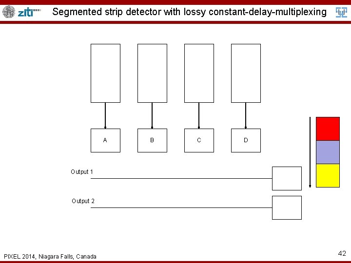
Segmented strip detector with lossy constant-delay-multiplexing A B C D Output 1 Output 2 PIXEL 2014, Niagara Falls, Canada 42

Segmented strip detector with lossy constant-delay-multiplexing y 5 A B C D Output 1 Output 2 PIXEL 2014, Niagara Falls, Canada 43

Segmented strip detector with lossy constant-delay-multiplexing y 5 0 A B 0 C 5 1 D Output 1 Output 2 PIXEL 2014, Niagara Falls, Canada 44

Segmented strip detector with lossy constant-delay-multiplexing y 5 0 Output 1 A B 0 C 5 1 D C 5 Output 2 PIXEL 2014, Niagara Falls, Canada 45

Segmented strip detector with lossy constant-delay-multiplexing A B C D Output 1 Output 2 PIXEL 2014, Niagara Falls, Canada 46

Segmented strip detector with lossy constant-delay-multiplexing y 1 y 4 A B C D Output 1 Output 2 PIXEL 2014, Niagara Falls, Canada 47

Segmented strip detector with lossy constant-delay-multiplexing y 1 y 4 0 A 1 1 B C D 4 2 Output 1 Output 2 PIXEL 2014, Niagara Falls, Canada 48

Segmented strip detector with lossy constant-delay-multiplexing y 1 y 4 0 Output 1 Output 2 PIXEL 2014, Niagara Falls, Canada A 1 1 B C D 4 2 A 1 D 4 49

Segmented strip detector with lossy constant-delay-multiplexing A B C D Output 1 Output 2 PIXEL 2014, Niagara Falls, Canada 50

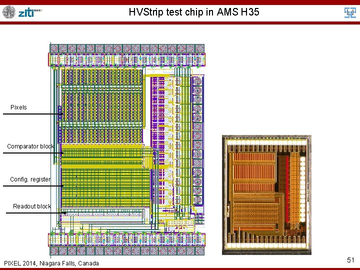
HVStrip test chip in AMS H 35 Pixels Comparator block Config. register Readout block PIXEL 2014, Niagara Falls, Canada 51

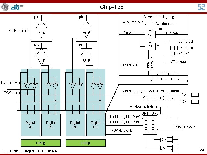
Chip-Top pix Comp out rising edge 40 MHz clock Active pixels amp pix Parity in Comp out pix demux amp Digital RO clock Sync hit Addr amp Normal comp. Synchronizer Sync hit Parity out xor Address line 1 Address line 2 cn ctw Comparator (time walk compensated) TWC comp. Comparator (normal) Analog multiplexer config PIXEL 2014, Niagara Falls, Canada Digital RO 40 MHz clock serializer Digital RO SR 1 SR 2 6 -bit address, hit 1, Par. Out 6 -bit address, hit 2, Par. Out 320 MHz clock config 52

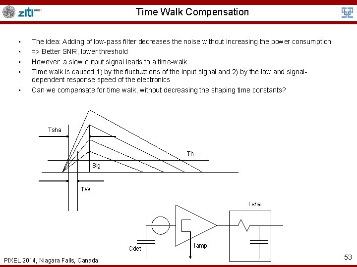
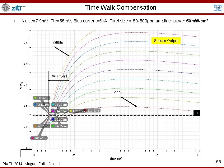
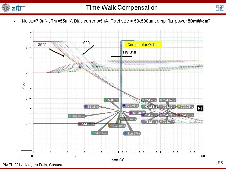
Time Walk Compensation • • • The idea: Adding of low-pass filter decreases the noise without increasing the power consumption => Better SNR, lower threshold However: a slow output signal leads to a time-walk Time walk is caused 1) by the fluctuations of the input signal and 2) by the low and signaldependent response speed of the electronics Can we compensate for time walk, without decreasing the shaping time constants? Tsha Th Sig TW Tsha Cdet PIXEL 2014, Niagara Falls, Canada Iamp 53

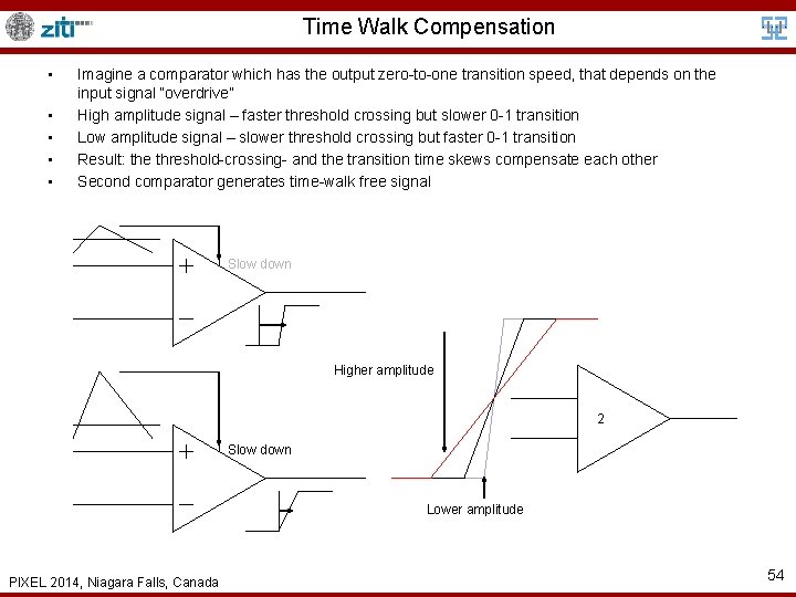
Time Walk Compensation • • • Imagine a comparator which has the output zero-to-one transition speed, that depends on the input signal “overdrive” High amplitude signal – faster threshold crossing but slower 0 -1 transition Low amplitude signal – slower threshold crossing but faster 0 -1 transition Result: the threshold-crossing- and the transition time skews compensate each other Second comparator generates time-walk free signal Slow down Higher amplitude 2 Slow down Lower amplitude PIXEL 2014, Niagara Falls, Canada 54

Time Walk Compensation • Noise=7. 9 m. V, Thr=55 m. V, Bias current=5µA, Pixel size = 50 x 500µm, amplifier power 50 m. W/cm 2 Shaper Output 3600 e TW 116 ns 900 e PIXEL 2014, Niagara Falls, Canada 55

Time Walk Compensation • Noise=7. 9 m. V, Thr=55 m. V, Bias current=5µA, Pixel size = 50 x 500µm, amplifier power 50 m. W/cm 2 3600 e 900 e Comparator Output TW 8 ns PIXEL 2014, Niagara Falls, Canada 56

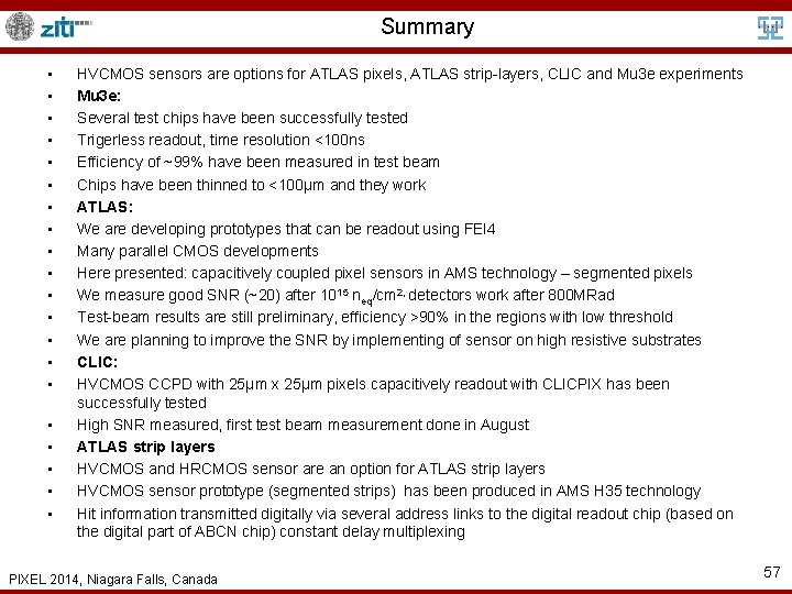
Summary • • • • • HVCMOS sensors are options for ATLAS pixels, ATLAS strip-layers, CLIC and Mu 3 e experiments Mu 3 e: Several test chips have been successfully tested Trigerless readout, time resolution <100 ns Efficiency of ~99% have been measured in test beam Chips have been thinned to <100μm and they work ATLAS: We are developing prototypes that can be readout using FEI 4 Many parallel CMOS developments Here presented: capacitively coupled pixel sensors in AMS technology – segmented pixels We measure good SNR (~20) after 1015 neq/cm 2, detectors work after 800 MRad Test-beam results are still preliminary, efficiency >90% in the regions with low threshold We are planning to improve the SNR by implementing of sensor on high resistive substrates CLIC: HVCMOS CCPD with 25μm x 25μm pixels capacitively readout with CLICPIX has been successfully tested High SNR measured, first test beam measurement done in August ATLAS strip layers HVCMOS and HRCMOS sensor are an option for ATLAS strip layers HVCMOS sensor prototype (segmented strips) has been produced in AMS H 35 technology Hit information transmitted digitally via several address links to the digital readout chip (based on the digital part of ABCN chip) constant delay multiplexing PIXEL 2014, Niagara Falls, Canada 57

Thank you! PIXEL 2014, Niagara Falls, Canada

Backup slides PIXEL 2014, Niagara Falls, Canada

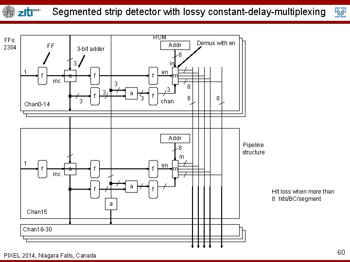
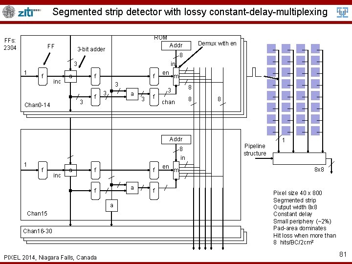
Segmented strip detector with lossy constant-delay-multiplexing ROM FFs: 2304 FF 8 3 1 f inc in f a f 3 3 Chan 0 -14 Demux with en Addr 3 -bit adder f 3 a 3 f en m 3 8 chan 8 8 Addr 8 in 1 f inc a f f a f en Pipeline structure m Hit loss when more than 8 hits/BC/segment Chan 15 Chan 16 -30 PIXEL 2014, Niagara Falls, Canada 60

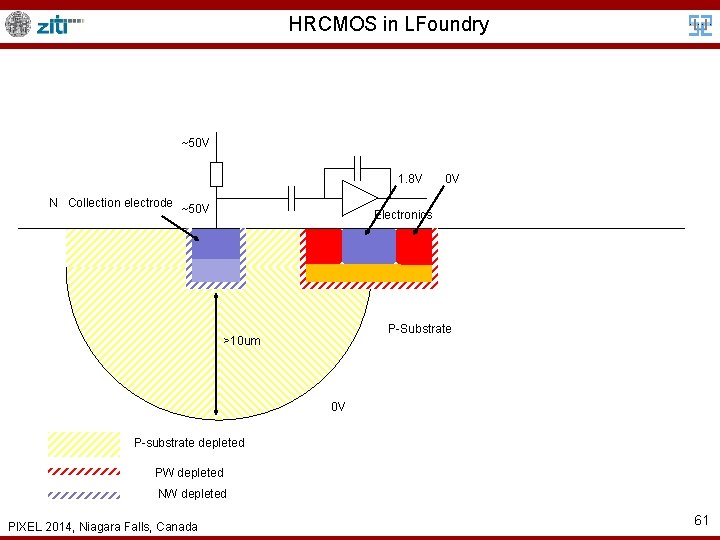
HRCMOS in LFoundry ~50 V 1. 8 V N Collection electrode ~50 V 0 V Electronics P-Substrate >10 um 0 V P-substrate depleted PW depleted NW depleted PIXEL 2014, Niagara Falls, Canada 61

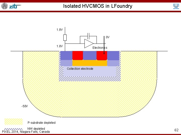
Isolated HVCMOS in LFoundry 1. 8 V 0 V 1. 8 V Electronics Collection electrode -50 V P-substrate depleted NW depleted PIXEL 2014, Niagara Falls, Canada 62

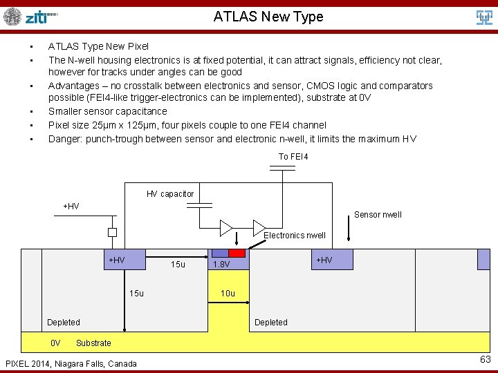
ATLAS New Type • • • ATLAS Type New Pixel The N-well housing electronics is at fixed potential, it can attract signals, efficiency not clear, however for tracks under angles can be good Advantages – no crosstalk between electronics and sensor, CMOS logic and comparators possible (FEI 4 -like trigger-electronics can be implemented), substrate at 0 V Smaller sensor capacitance Pixel size 25µm x 125µm, four pixels couple to one FEI 4 channel Danger: punch-trough between sensor and electronic n-well, it limits the maximum HV To FEI 4 HV capacitor +HV Sensor nwell Electronics nwell +HV 15 u Depleted 0 V +HV 1. 8 V 10 u Depleted Substrate PIXEL 2014, Niagara Falls, Canada 63

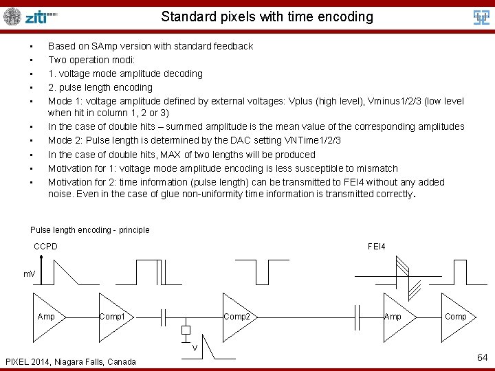
Standard pixels with time encoding • • • Based on SAmp version with standard feedback Two operation modi: 1. voltage mode amplitude decoding 2. pulse length encoding Mode 1: voltage amplitude defined by external voltages: Vplus (high level), Vminus 1/2/3 (low level when hit in column 1, 2 or 3) In the case of double hits – summed amplitude is the mean value of the corresponding amplitudes Mode 2: Pulse length is determined by the DAC setting VNTime 1/2/3 In the case of double hits, MAX of two lengths will be produced Motivation for 1: voltage mode amplitude encoding is less susceptible to mismatch Motivation for 2: time information (pulse length) can be transmitted to FEI 4 without any added noise. Even in the case of glue non-uniformity time information is transmitted correctly. • • • Pulse length encoding - principle CCPD FEI 4 m. V Amp Comp 1 Comp 2 V PIXEL 2014, Niagara Falls, Canada Amp Comp 64

CCPDv 4 Pixel structures implemented in CCPDv 4 SAmp: Standard pixels (as in CCPDv 3 -1, contain comparator and tune DAC) with the current-mode amplitude coding – several improvements Stime: Standard pixels with (new) voltage-mode amplitude coding or the pulse length coding N: “New. Pixels” – the pixels with separated electronic and electrode, sub pixel size 25 um x 125 um (as in CCPDv 3 contain comparator and tune DAC) A: New: Analog pixels - size 25 um x 350 um – contain only amplifier - electronics similar as in CLIC pixels (CCPDv 3). New analog summing scheme. SAmp STime Analog pixels 25 um 33 um s 1 s 3 s 2 PIXEL 2014, Niagara Falls, Canada 65

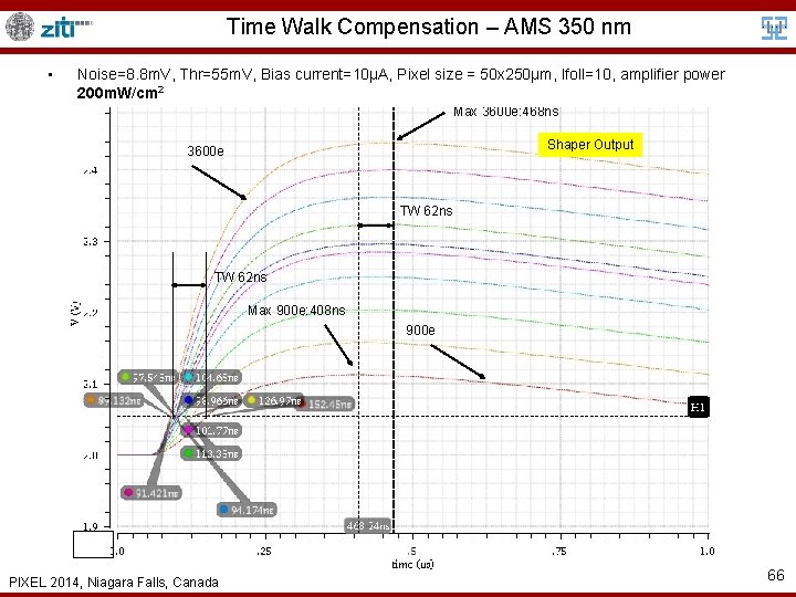
Time Walk Compensation – AMS 350 nm • Noise=8. 8 m. V, Thr=55 m. V, Bias current=10µA, Pixel size = 50 x 250µm, Ifoll=10, amplifier power 200 m. W/cm 2 Max 3600 e: 468 ns Shaper Output 3600 e TW 62 ns Max 900 e: 408 ns 900 e PIXEL 2014, Niagara Falls, Canada 66

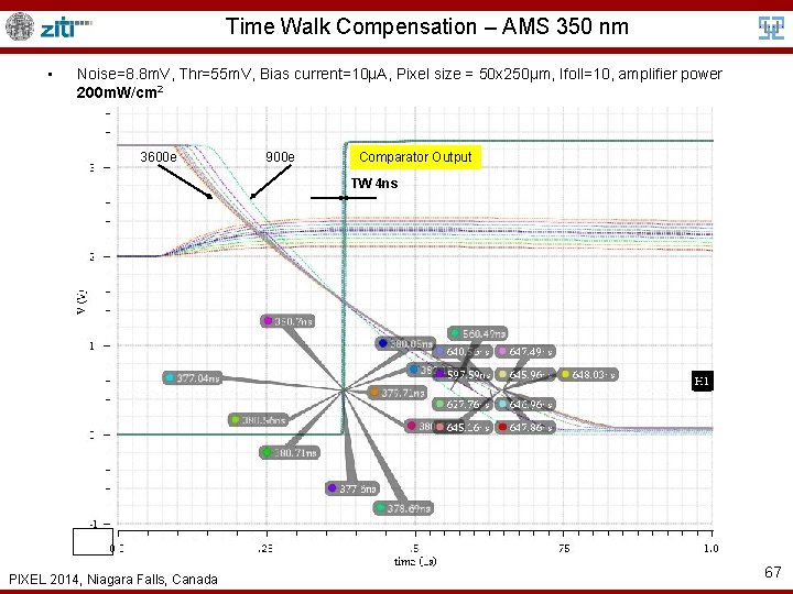
Time Walk Compensation – AMS 350 nm • Noise=8. 8 m. V, Thr=55 m. V, Bias current=10µA, Pixel size = 50 x 250µm, Ifoll=10, amplifier power 200 m. W/cm 2 3600 e 900 e Comparator Output TW 4 ns PIXEL 2014, Niagara Falls, Canada 67

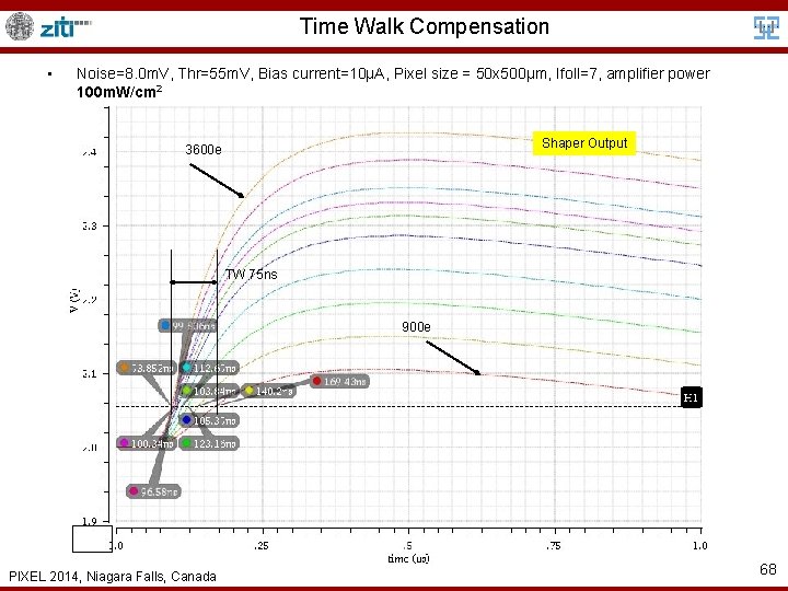
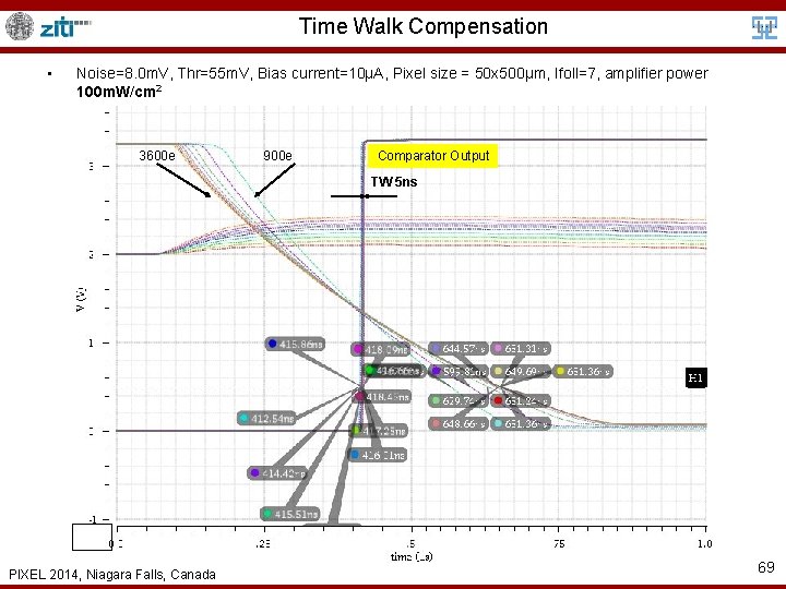
Time Walk Compensation • Noise=8. 0 m. V, Thr=55 m. V, Bias current=10µA, Pixel size = 50 x 500µm, Ifoll=7, amplifier power 100 m. W/cm 2 Shaper Output 3600 e TW 75 ns 900 e PIXEL 2014, Niagara Falls, Canada 68

Time Walk Compensation • Noise=8. 0 m. V, Thr=55 m. V, Bias current=10µA, Pixel size = 50 x 500µm, Ifoll=7, amplifier power 100 m. W/cm 2 3600 e 900 e Comparator Output TW 5 ns PIXEL 2014, Niagara Falls, Canada 69

AMS TSV process PIXEL 2014, Niagara Falls, Canada 70

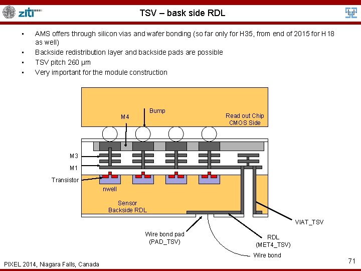
TSV – bask side RDL • • AMS offers through silicon vias and wafer bonding (so far only for H 35, from end of 2015 for H 18 as well) Backside redistribution layer and backside pads are possible TSV pitch 260 µm Very important for the module construction Bump M 4 Read out Chip CMOS Side M 3 M 1 Transistor nwell Sensor Backside RDL VIAT_TSV Wire bond pad (PAD_TSV) RDL (MET 4_TSV) Wire bond PIXEL 2014, Niagara Falls, Canada 71

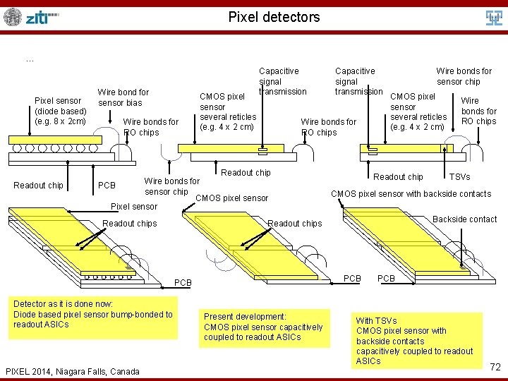
Pixel detectors … Pixel sensor (diode based) (e. g. 8 x 2 cm) Readout chip Wire bond for sensor bias Wire bonds for RO chips CMOS pixel sensor several reticles (e. g. 4 x 2 cm) Capacitive signal transmission Wire bonds for RO chips Readout chip Wire bonds for PCB sensor chip CMOS pixel sensor Pixel sensor Readout chips PIXEL 2014, Niagara Falls, Canada Wire bonds for sensor chip CMOS pixel sensor several reticles (e. g. 4 x 2 cm) Readout chip TSVs Backside contact PCB Present development: CMOS pixel sensor capacitively coupled to readout ASICs Wire bonds for RO chips CMOS pixel sensor with backside contacts Readout chips PCB Detector as it is done now: Diode based pixel sensor bump-bonded to readout ASICs Capacitive signal transmission PCB With TSVs CMOS pixel sensor with backside contacts capacitively coupled to readout ASICs 72

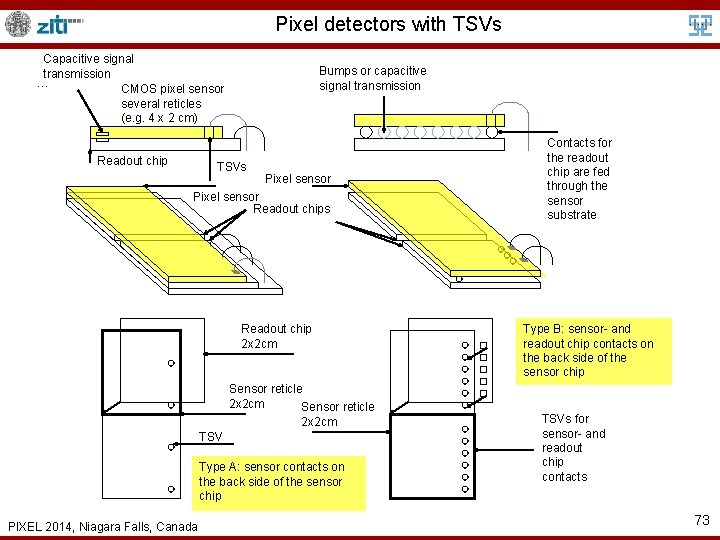
Pixel detectors with TSVs Capacitive signal transmission … CMOS pixel sensor several reticles (e. g. 4 x 2 cm) Readout chip Bumps or capacitive signal transmission TSVs Pixel sensor Readout chips Readout chip 2 x 2 cm Sensor reticle 2 x 2 cm TSV Type A: sensor contacts on the back side of the sensor chip PIXEL 2014, Niagara Falls, Canada Contacts for the readout chip are fed through the sensor substrate Type B: sensor- and readout chip contacts on the back side of the sensor chip TSVs for sensor- and readout chip contacts 73

Detectors is advanced CMOS: HRCMOS PIXEL 2014, Niagara Falls, Canada

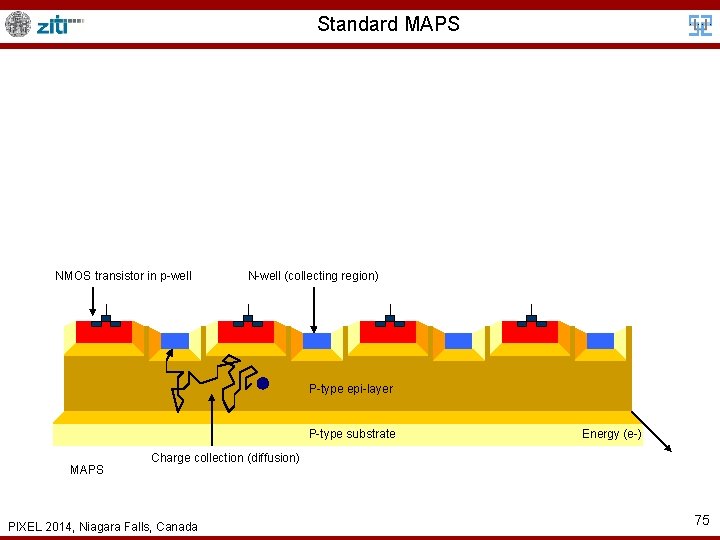
Standard MAPS NMOS transistor in p-well N-well (collecting region) P-type epi-layer P-type substrate MAPS Energy (e-) Charge collection (diffusion) PIXEL 2014, Niagara Falls, Canada 75

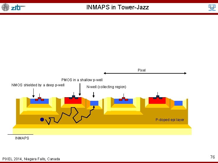
INMAPS in Tower-Jazz Pixel PMOS in a shallow p-well NMOS shielded by a deep p-well N-well (collecting region) P-doped epi layer INMAPS PIXEL 2014, Niagara Falls, Canada 76

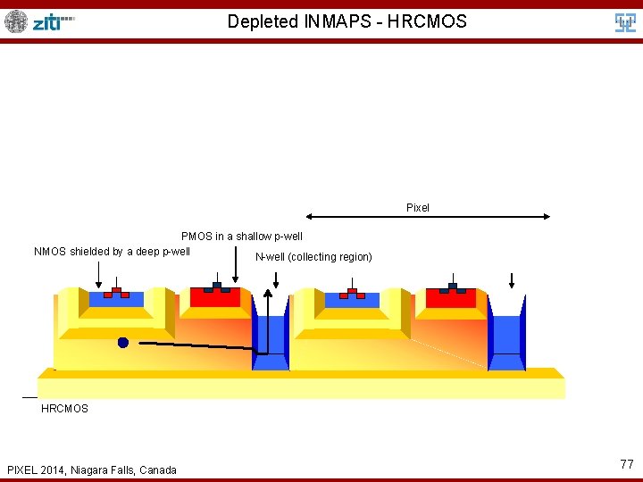
Depleted INMAPS - HRCMOS Pixel PMOS in a shallow p-well NMOS shielded by a deep p-well N-well (collecting region) HRCMOS PIXEL 2014, Niagara Falls, Canada 77

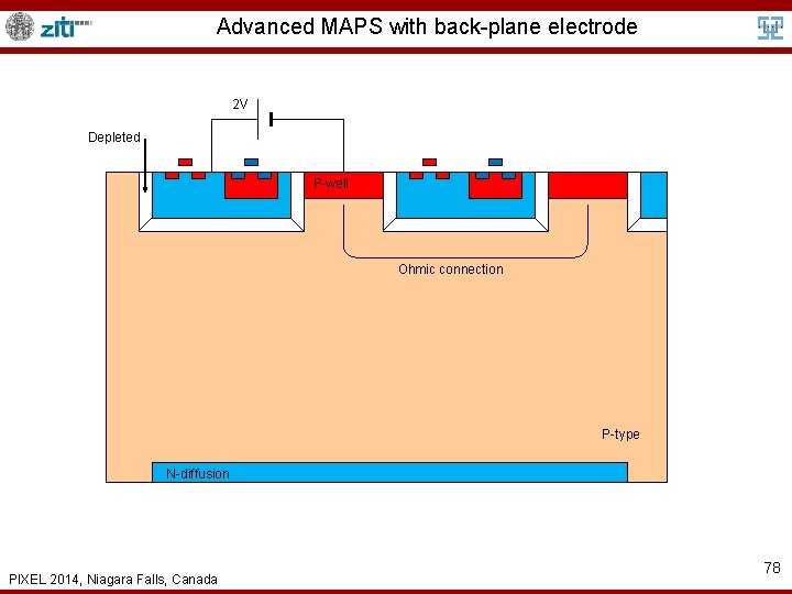
Advanced MAPS with back-plane electrode 2 V Depleted P-well Ohmic connection P-type N-diffusion PIXEL 2014, Niagara Falls, Canada 78

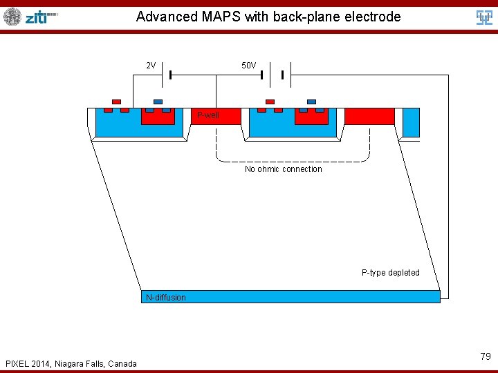
Advanced MAPS with back-plane electrode 2 V 50 V P-well No ohmic connection P-type depleted N-diffusion PIXEL 2014, Niagara Falls, Canada 79

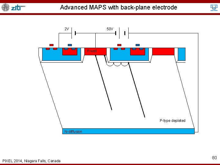
Advanced MAPS with back-plane electrode 2 V 50 V P-well P-type depleted N-diffusion PIXEL 2014, Niagara Falls, Canada 80

Segmented strip detector with lossy constant-delay-multiplexing ROM FFs: 2304 FF 8 3 1 f inc in f a f 3 3 Chan 0 -14 Demux with en Addr 3 -bit adder f 3 a 3 f en m 3 8 chan 8 8 Addr 8 in 1 f inc a f f a Chan 15 Chan 16 -30 PIXEL 2014, Niagara Falls, Canada f en m Pipeline structure 1 8 x 8 Pixel size 40 x 800 Segmented strip Output width 8 x 8 Constant delay Small periphery (~2%) Pad-area dominates Hit loss when more than 8 hits/BC/2 cm 2 81

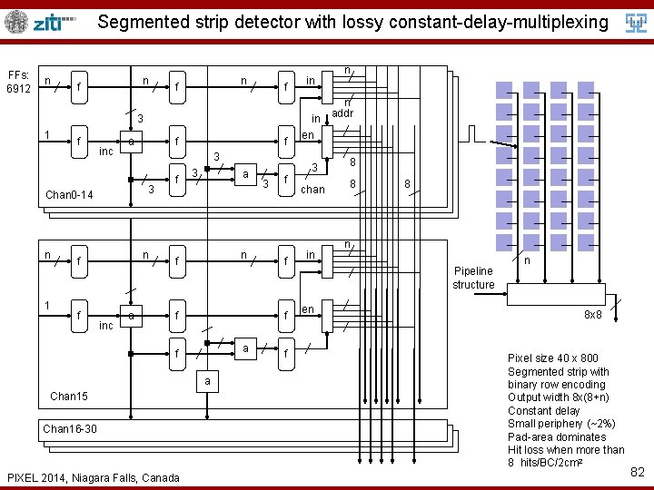
Segmented strip detector with lossy constant-delay-multiplexing FFs: 6912 n n f f 3 1 f inc n 1 f 3 n inc f 3 f f in a Chan 0 -14 a in f 3 a n f f a a Chan 16 -30 PIXEL 2014, Niagara Falls, Canada f f Chan 15 3 f n n addr en 3 8 chan 8 in 8 n Pipeline structure en n 8 x 8 Pixel size 40 x 800 Segmented strip with binary row encoding Output width 8 x(8+n) Constant delay Small periphery (~2%) Pad-area dominates Hit loss when more than 8 hits/BC/2 cm 2 82

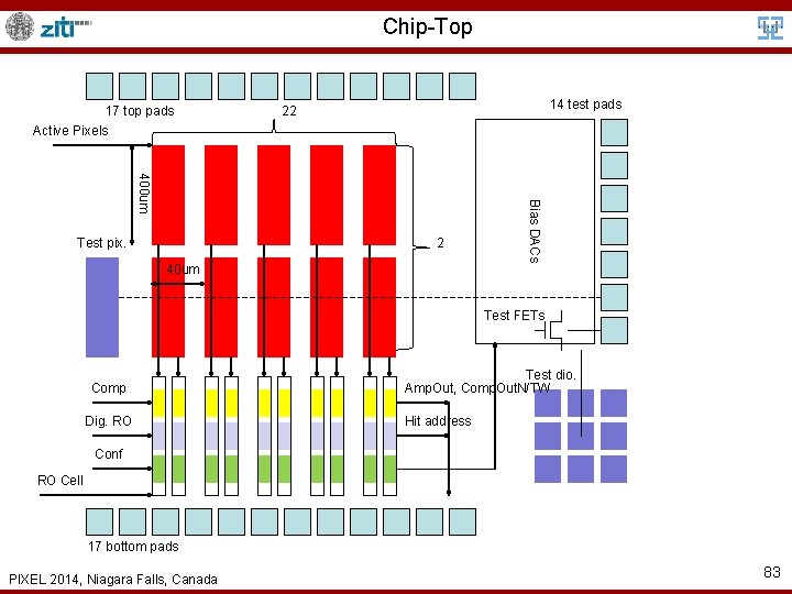
Chip-Top 17 top pads Active Pixels 14 test pads 22 2 40 um Bias DACs 400 um Test pix. Test FETs Comp Dig. RO Test dio. Amp. Out, Comp. Out. N/TW Hit address Conf RO Cell 17 bottom pads PIXEL 2014, Niagara Falls, Canada 83