Monolithic pixel sensors Ivan Peri TALENT Summer School


- Slides: 85

Monolithic pixel sensors Ivan Perić TALENT Summer School, June 2013 1

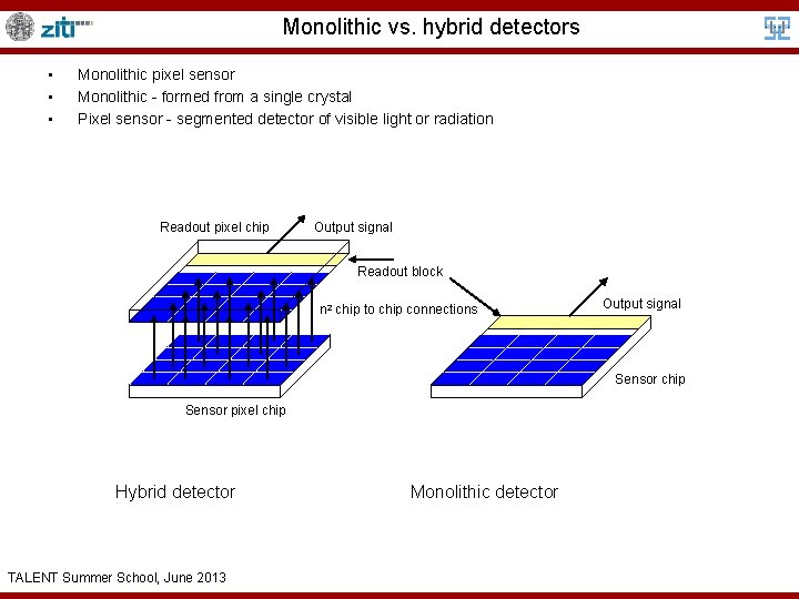
Monolithic vs. hybrid detectors • • • Monolithic pixel sensor Monolithic - formed from a single crystal Pixel sensor - segmented detector of visible light or radiation Readout pixel chip Output signal Readout block n 2 chip to chip connections Output signal Sensor chip Sensor pixel chip Hybrid detector TALENT Summer School, June 2013 Monolithic detector

Overview of monolithic sensors • • Monolithic pixel sensors – three classes 1) Pixel sensors implemented in commercial CMOS technologies 2) Special monolithic technologies (DEPFETs, SOI-detectors) 3) Monolithic sensors obtained by 3 D integration TALENT Summer School, June 2013

Commercial (C)MOS monolithic pixel sensors TALENT Summer School, June 2013 4

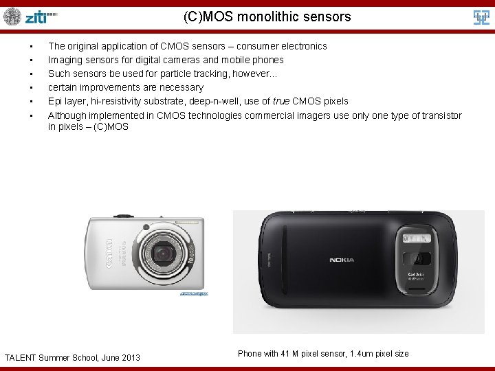
(C)MOS monolithic sensors • • • The original application of CMOS sensors – consumer electronics Imaging sensors for digital cameras and mobile phones Such sensors be used for particle tracking, however… certain improvements are necessary Epi layer, hi-resistivity substrate, deep-n-well, use of true CMOS pixels Although implemented in CMOS technologies commercial imagers use only one type of transistor in pixels – (C)MOS TALENT Summer School, June 2013 Phone with 41 M pixel sensor, 1. 4 um pixel size

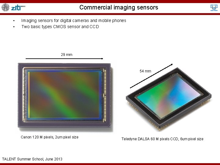
Commercial imaging sensors • • Imaging sensors for digital cameras and mobile phones Two basic types CMOS sensor and CCD 29 mm 54 mm Canon 120 M pixels, 2 um pixel size TALENT Summer School, June 2013 Teledyne DALSA 60 M pixels CCD, 6 um pixel size

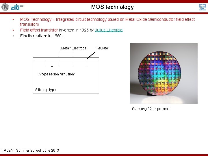
MOS technology • • • MOS Technology – Integrated circuit technology based on Metal Oxide Semiconductor field effect transistors Field effect transistor invented in 1925 by Julius Lilienfeld Finally realized in 1960 s „Metal“ Electrode Insulator n type region “diffusion” Silicon p type Samsung 32 nm process TALENT Summer School, June 2013

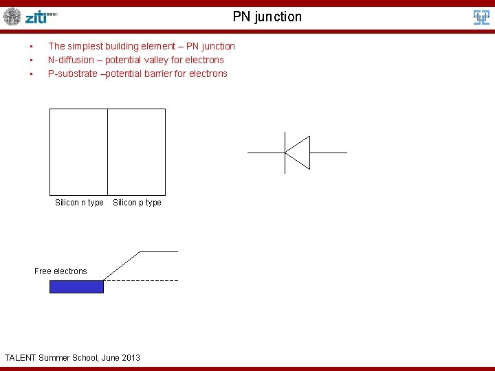
PN junction • • • The simplest building element – PN junction N-diffusion – potential valley for electrons P-substrate –potential barrier for electrons Silicon n type Silicon p type Free electrons TALENT Summer School, June 2013

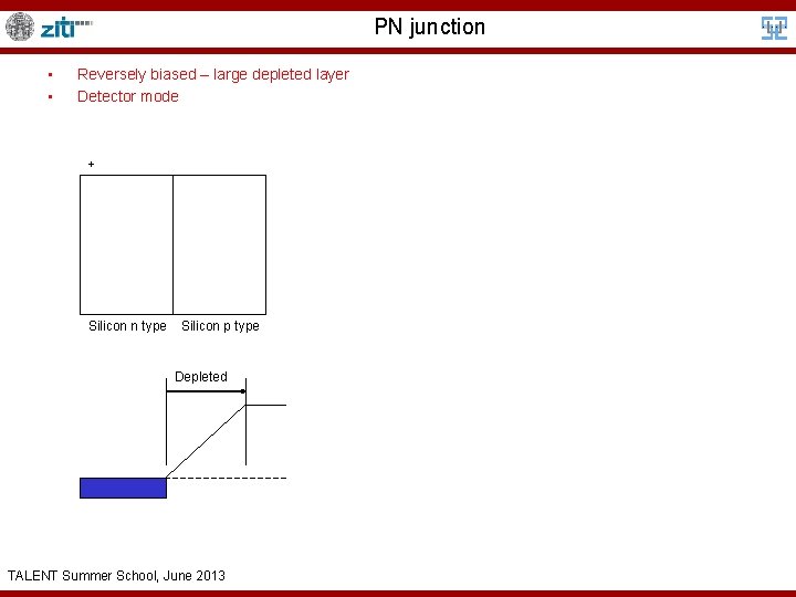
PN junction • • Reversely biased – large depleted layer Detector mode + Silicon n type Silicon p type Depleted TALENT Summer School, June 2013

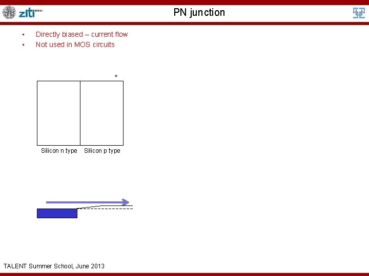
PN junction • • Directly biased – current flow Not used in MOS circuits + Silicon n type Silicon p type TALENT Summer School, June 2013

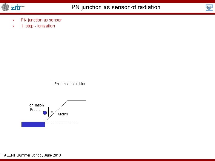
PN junction as sensor of radiation • • PN junction as sensor 1. step - ionization Photons or particles Ionisation Free e. Atoms TALENT Summer School, June 2013

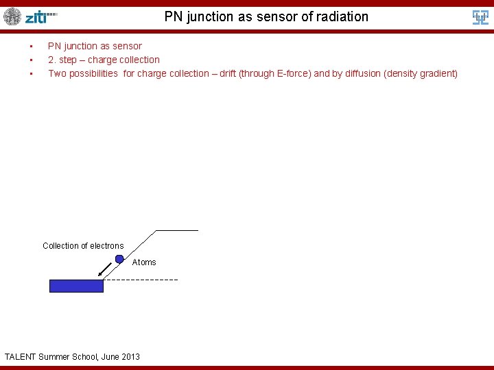
PN junction as sensor of radiation • • • PN junction as sensor 2. step – charge collection Two possibilities for charge collection – drift (through E-force) and by diffusion (density gradient) Collection of electrons Atoms TALENT Summer School, June 2013

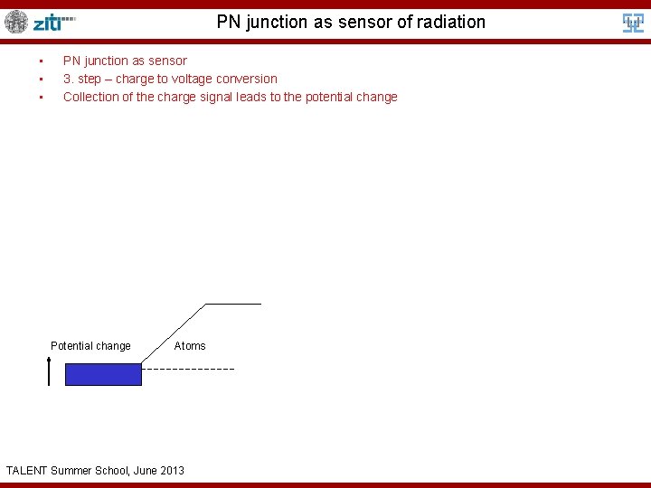
PN junction as sensor of radiation • • • PN junction as sensor 3. step – charge to voltage conversion Collection of the charge signal leads to the potential change Potential change Atoms TALENT Summer School, June 2013

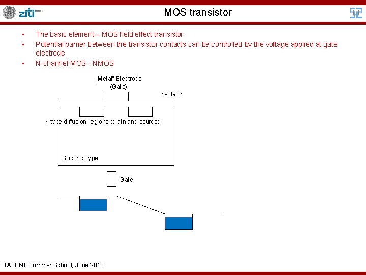
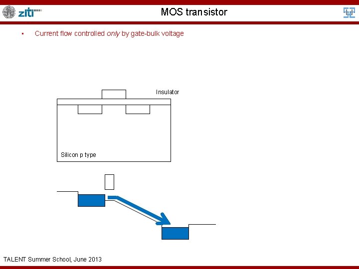
MOS transistor • • • The basic element – MOS field effect transistor Potential barrier between the transistor contacts can be controlled by the voltage applied at gate electrode N-channel MOS - NMOS „Metal“ Electrode (Gate) Insulator N-type diffusion-regions (drain and source) Silicon p type Gate TALENT Summer School, June 2013

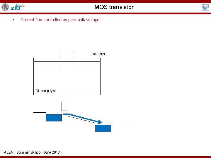
MOS transistor • Current flow controlled by gate-bulk voltage Insulator Silicon p type TALENT Summer School, June 2013

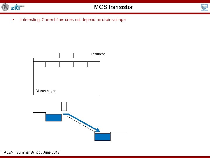
MOS transistor • Interesting: Current flow does not depend on drain voltage Insulator Silicon p type TALENT Summer School, June 2013

MOS transistor • Current flow controlled only by gate-bulk voltage Insulator Silicon p type TALENT Summer School, June 2013

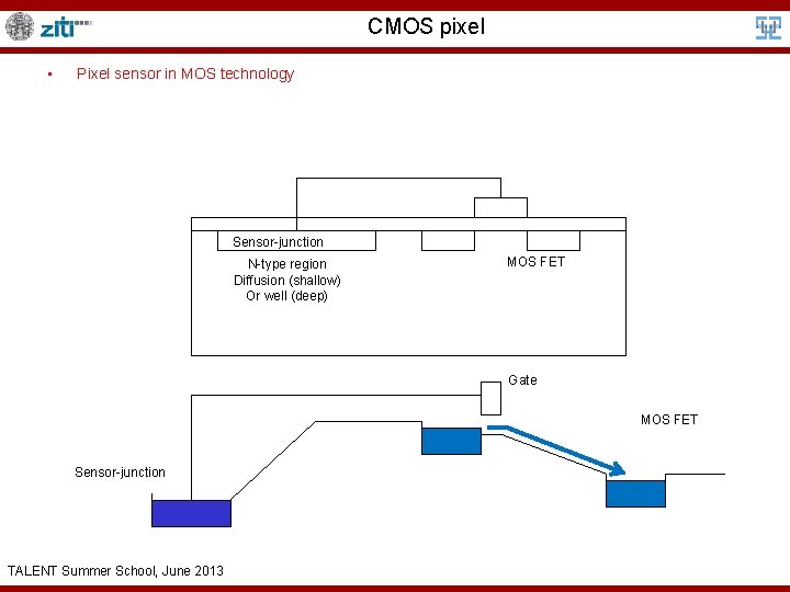
CMOS pixel • Pixel sensor in MOS technology Sensor-junction N-type region Diffusion (shallow) Or well (deep) MOS FET Gate MOS FET Sensor-junction TALENT Summer School, June 2013

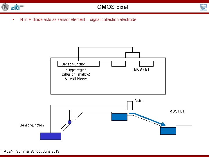
CMOS pixel • N in P diode acts as sensor element – signal collection electrode Sensor-junction N-type region Diffusion (shallow) Or well (deep) MOS FET Gate MOS FET Sensor-junction TALENT Summer School, June 2013

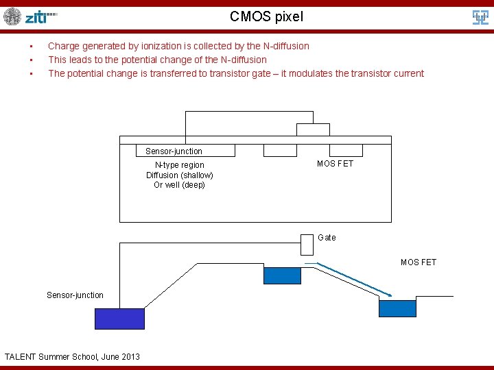
CMOS pixel • • • Charge generated by ionization is collected by the N-diffusion This leads to the potential change of the N-diffusion The potential change is transferred to transistor gate – it modulates the transistor current Sensor-junction N-type region Diffusion (shallow) Or well (deep) MOS FET Gate MOS FET Sensor-junction TALENT Summer School, June 2013

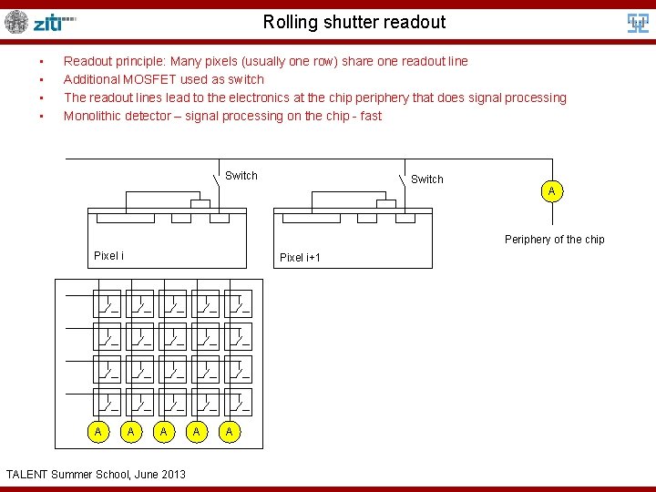
Rolling shutter readout • • Readout principle: Many pixels (usually one row) share one readout line Additional MOSFET used as switch The readout lines lead to the electronics at the chip periphery that does signal processing Monolithic detector – signal processing on the chip - fast Switch A Periphery of the chip Pixel i A Pixel i+1 A A TALENT Summer School, June 2013 A A

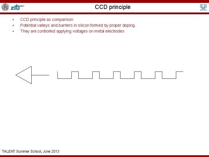
CCD principle • • • CCD principle as comparison Potential valleys and barriers in silicon formed by proper doping. They are controlled applying voltages on metal electrodes TALENT Summer School, June 2013

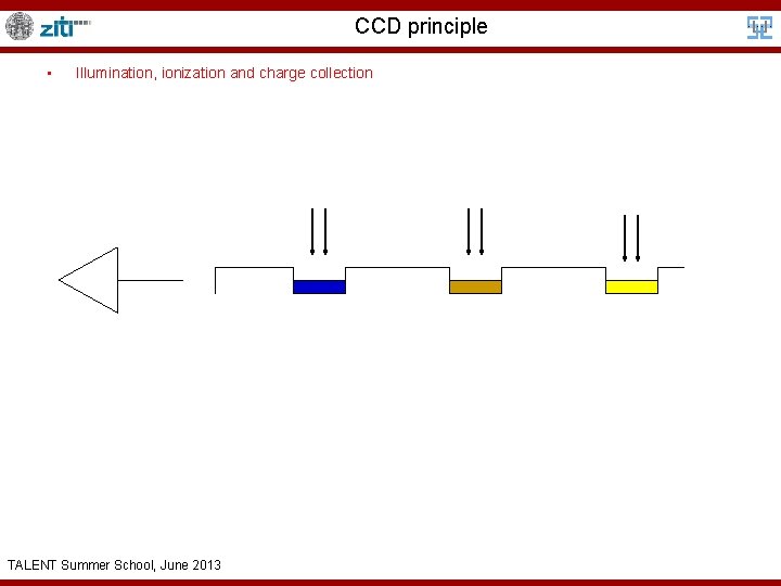
CCD principle • Illumination, ionization and charge collection TALENT Summer School, June 2013

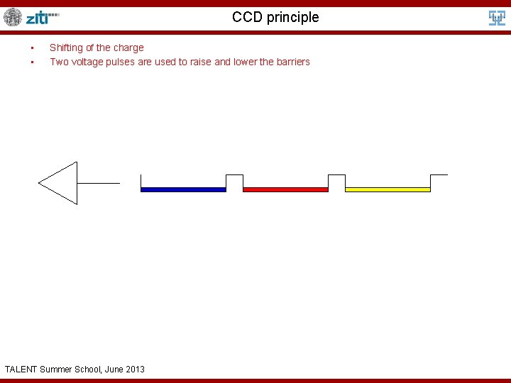
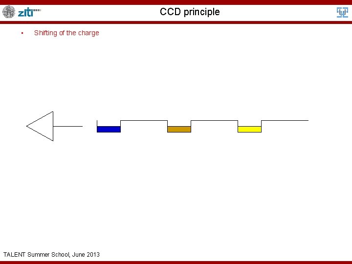
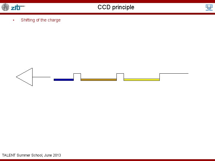
CCD principle • • Shifting of the charge Two voltage pulses are used to raise and lower the barriers TALENT Summer School, June 2013

CCD principle • Shifting of the charge TALENT Summer School, June 2013

CCD principle • Shifting of the charge TALENT Summer School, June 2013

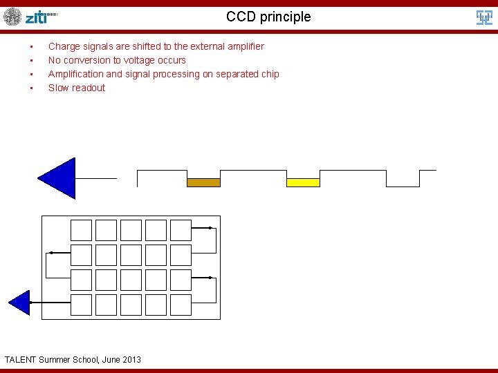
CCD principle • • Charge signals are shifted to the external amplifier No conversion to voltage occurs Amplification and signal processing on separated chip Slow readout TALENT Summer School, June 2013

(C)MOS monolithic pixel sensors for particle tracking TALENT Summer School, June 2013 28

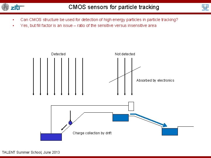
CMOS sensors for particle tracking • • Can CMOS structure be used for detection of high energy particles in particle tracking? Yes, but fill factor is an issue – ratio of the sensitive versus insensitive area Detected Not detected Absorbed by electronics Charge collection by drift TALENT Summer School, June 2013

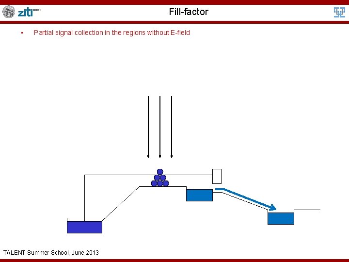
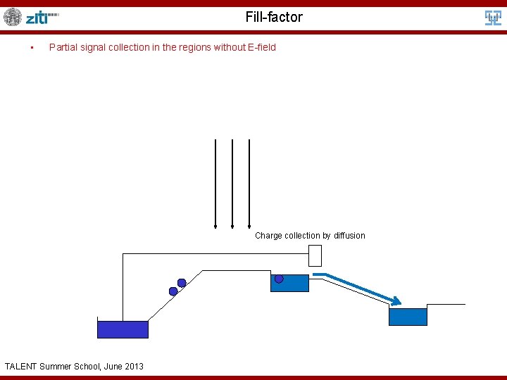
Fill-factor • Partial signal collection in the regions without E-field TALENT Summer School, June 2013

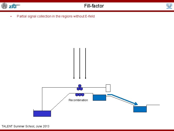
Fill-factor • Partial signal collection in the regions without E-field Recombination TALENT Summer School, June 2013

Overview • Partial signal collection in the regions without E-field Recombination TALENT Summer School, June 2013

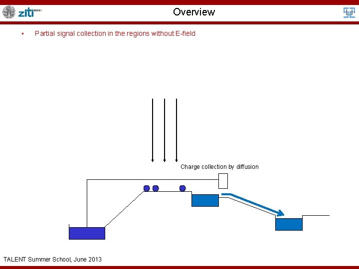
Overview • Partial signal collection in the regions without E-field Charge collection by diffusion TALENT Summer School, June 2013

Fill-factor • Partial signal collection in the regions without E-field Charge collection by diffusion TALENT Summer School, June 2013

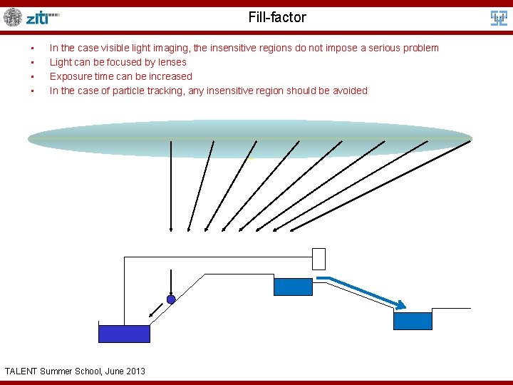
Fill-factor • • In the case visible light imaging, the insensitive regions do not impose a serious problem Light can be focused by lenses Exposure time can be increased In the case of particle tracking, any insensitive region should be avoided TALENT Summer School, June 2013

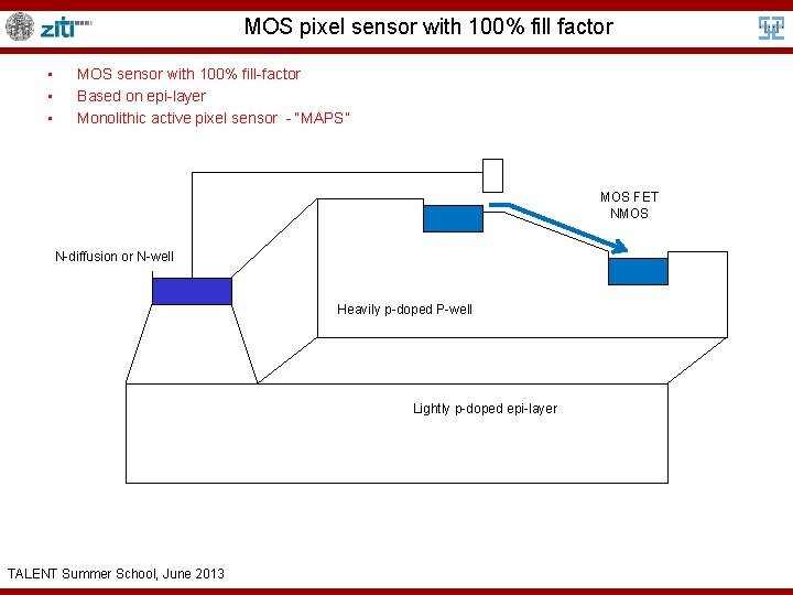
MOS pixel sensor with 100% fill factor • • • MOS sensor with 100% fill-factor Based on epi-layer Monolithic active pixel sensor - “MAPS” MOS FET NMOS N-diffusion or N-well Heavily p-doped P-well Lightly p-doped epi-layer TALENT Summer School, June 2013

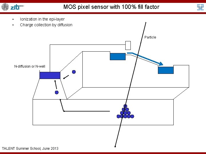
MOS pixel sensor with 100% fill factor • • Ionization in the epi-layer Charge collection by diffusion Particle N-diffusion or N-well TALENT Summer School, June 2013

MAPS TALENT Summer School, June 2013 38

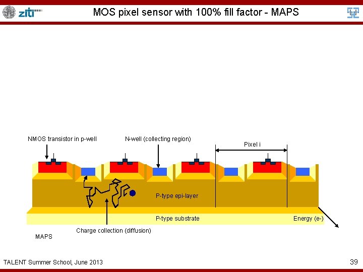
MOS pixel sensor with 100% fill factor - MAPS NMOS transistor in p-well N-well (collecting region) Pixel i P-type epi-layer P-type substrate MAPS Energy (e-) Charge collection (diffusion) TALENT Summer School, June 2013 39

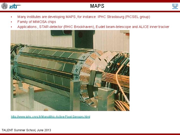
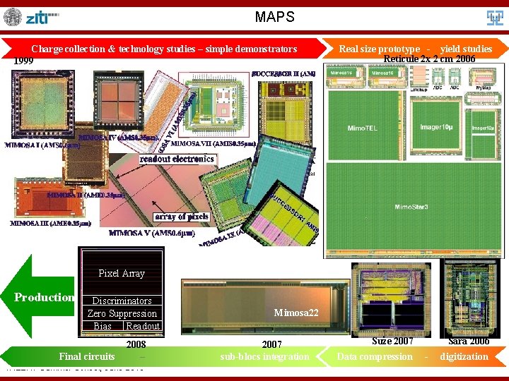
MAPS • • • Many institutes are developing MAPS, for instance: IPHC Strasbourg (PICSEL group) Family of MIMOSA chips Applications: , STAR-detector (RHIC Brookhaven), Eudet beam-telescope and ALICE inner tracker upgrade http: //www. iphc. cnrs. fr/Monolithic-Active-Pixel-Sensors. html TALENT Summer School, June 2013

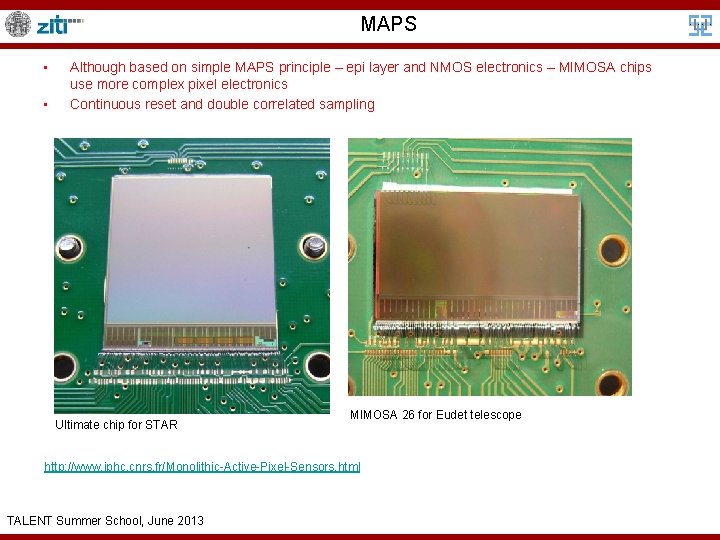
MAPS • • Although based on simple MAPS principle – epi layer and NMOS electronics – MIMOSA chips use more complex pixel electronics Continuous reset and double correlated sampling Ultimate chip for STAR MIMOSA 26 for Eudet telescope http: //www. iphc. cnrs. fr/Monolithic-Active-Pixel-Sensors. html TALENT Summer School, June 2013

MAPS Charge collection & technology studies – simple demonstrators 1999 Real size prototype - yield studies Reticule 2 x 2 cm 2006 Pixel Array Production Discriminators Zero Suppression Bias Readout Final circuits 2008 – TALENT Summer School, June 2013 Mimosa 22 2007 sub-blocs integration Suze 2007 Data compression Sara 2006 - digitization

Advanced CMOS pixel sensors with intelligent pixels TALENT Summer School, June 2013 43

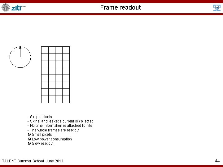
Frame readout - Simple pixels - Signal and leakage current is collected - No time information is attached to hits - The whole frames are readout Small pixels Low power consumption Slow readout TALENT Summer School, June 2013 44

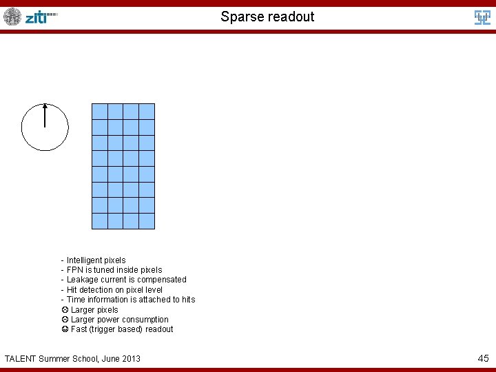
Sparse readout 3 6 9 9 - Intelligent pixels - FPN is tuned inside pixels - Leakage current is compensated - Hit detection on pixel level - Time information is attached to hits Larger pixels Larger power consumption Fast (trigger based) readout TALENT Summer School, June 2013 45

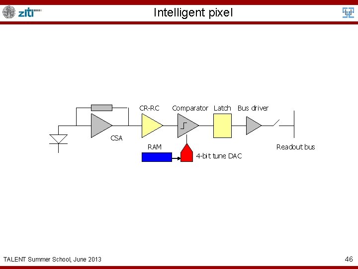
Intelligent pixel CR-RC Comparator Latch Bus driver CSA RAM Readout bus 4 -bit tune DAC TALENT Summer School, June 2013 46

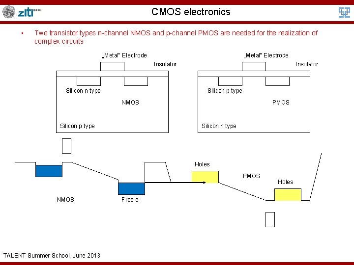
CMOS electronics • Two transistor types n-channel NMOS and p-channel PMOS are needed for the realization of complex circuits „Metal“ Electrode Insulator Silicon n type Insulator Silicon p type NMOS Silicon p type PMOS Silicon n type Holes PMOS NMOS TALENT Summer School, June 2013 Free e- Holes

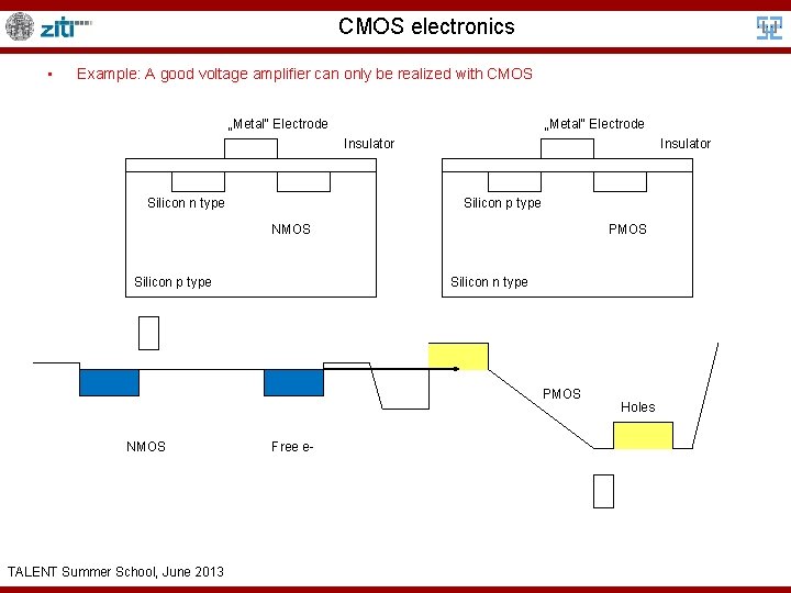
CMOS electronics • Example: A good voltage amplifier can only be realized with CMOS „Metal“ Electrode Insulator Silicon n type Insulator Silicon p type NMOS Silicon p type PMOS Silicon n type PMOS NMOS TALENT Summer School, June 2013 Free e- Holes

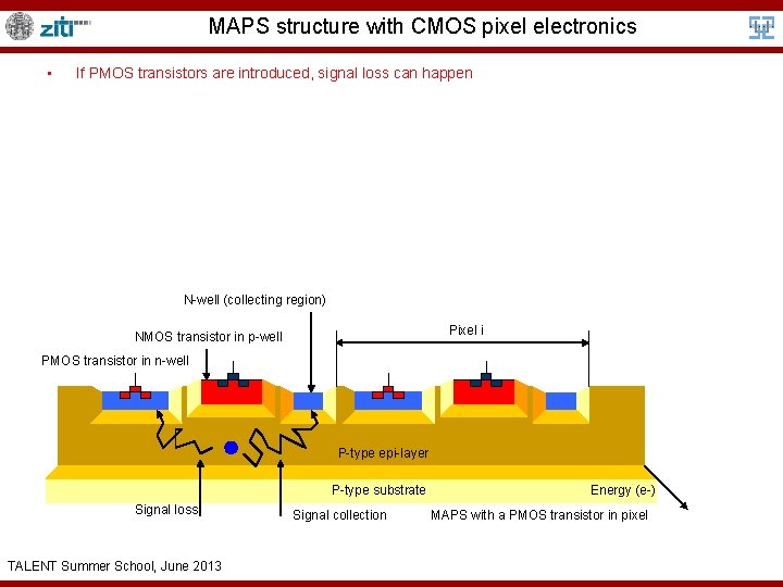
MAPS structure with CMOS pixel electronics • If PMOS transistors are introduced, signal loss can happen N-well (collecting region) Pixel i NMOS transistor in p-well PMOS transistor in n-well P-type epi-layer P-type substrate Signal loss TALENT Summer School, June 2013 Signal collection Energy (e-) MAPS with a PMOS transistor in pixel

Advanced structures: INMAPS TALENT Summer School, June 2013 50

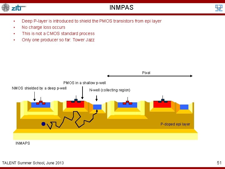
INMPAS • • Deep P-layer is introduced to shield the PMOS transistors from epi layer No charge loss occurs This is not a CMOS standard process Only one producer so far: Tower Jazz Pixel PMOS in a shallow p-well NMOS shielded by a deep p-well N-well (collecting region) P-doped epi layer INMAPS TALENT Summer School, June 2013 51

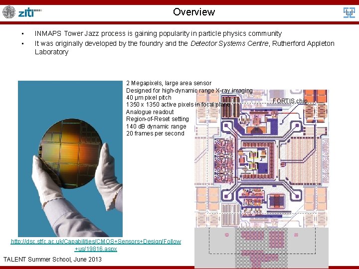
Overview • • INMAPS Tower Jazz process is gaining popularity in particle physics community It was originally developed by the foundry and the Detector Systems Centre, Rutherford Appleton Laboratory 2 Megapixels, large area sensor Designed for high-dynamic range X-ray imaging 40 µm pixel pitch 1350 x 1350 active pixels in focal plane Analogue readout Region-of-Reset setting 140 d. B dynamic range 20 frames per second http: //dsc. stfc. ac. uk/Capabilities/CMOS+Sensors+Design/Follow +us/19816. aspx TALENT Summer School, June 2013 FORTIS chip

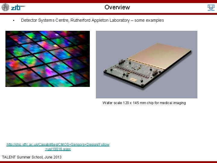
Overview • Detector Systems Centre, Rutherford Appleton Laboratory – some examples Wafer scale 120 x 145 mm chip for medical imaging http: //dsc. stfc. ac. uk/Capabilities/CMOS+Sensors+Design/Follow +us/19816. aspx TALENT Summer School, June 2013

Fast CMOS detectors based on drift charge collection: detectors in HVCMOS-processes and the CMOS processes with a high resistive wafer TALENT Summer School, June 2013 54

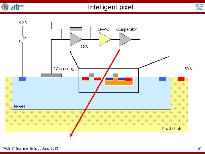
Drift based detector: HVMAPS • • HVMAPS rely on the charge collection by drift Fast charge collection – high radiation tolerance The key is the use of a high voltage n-well in a relatively highly doped substrate Pixel electronics is embedded in the n-well Two concepts: High Ohmic Monolithic Pixels - Le. PIX – relies on a special CMOS process with high resistive substrate (CERN, Geneve) HVCMOS (or smart diode arrays - SDAs) – use a commercial HVCMOS process (CPPM, CERN, Bonn, LBNL, Geneve, Göttingen, Manchester and Heidelberg) TALENT Summer School, June 2013 55

HVCMOS detectors (smart diode arrays) TALENT Summer School, June 2013 56

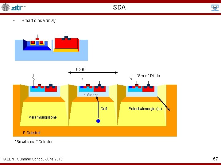
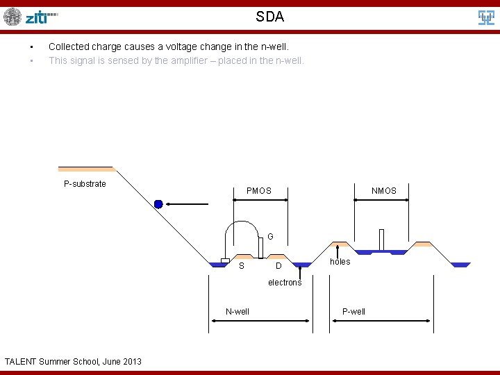
SDA • Smart diode array Pixel “Smart” Diode n-Wanne Drift Potentialenergie (e-) Verarmungszone P-Substrat “Smart diode” Detector TALENT Summer School, June 2013 57

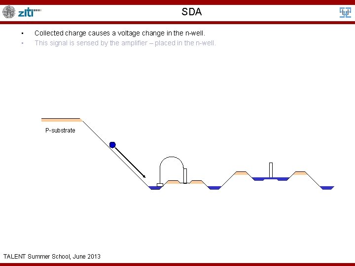
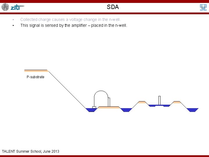
SDA • • Collected charge causes a voltage change in the n-well. This signal is sensed by the amplifier – placed in the n-well. P-substrate PMOS NMOS G S D holes electrons N-well TALENT Summer School, June 2013 P-well

SDA • • Collected charge causes a voltage change in the n-well. This signal is sensed by the amplifier – placed in the n-well. P-substrate TALENT Summer School, June 2013

SDA • • Collected charge causes a voltage change in the n-well. This signal is sensed by the amplifier – placed in the n-well. P-substrate TALENT Summer School, June 2013

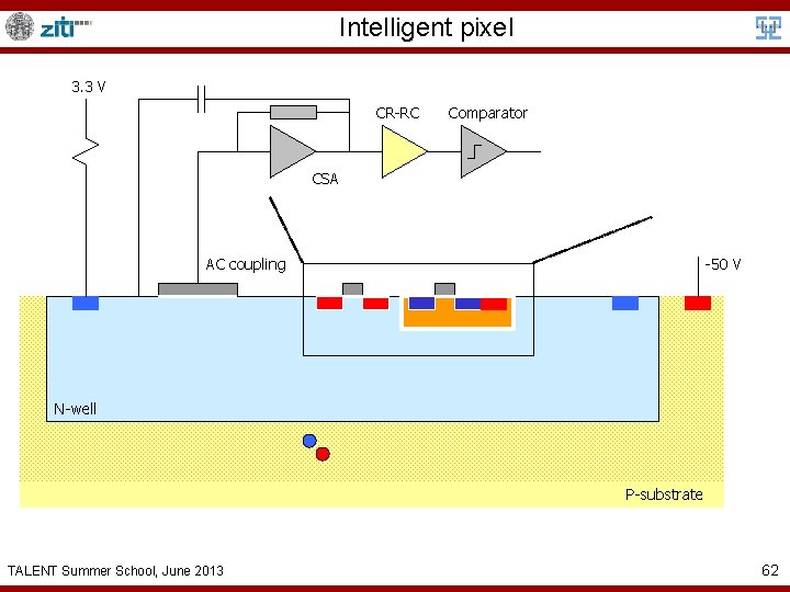
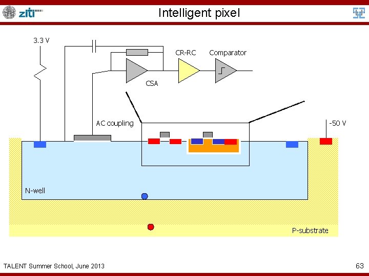
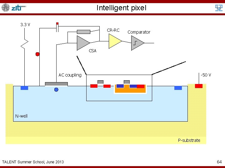
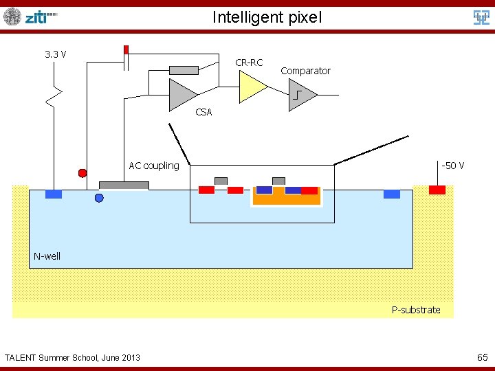
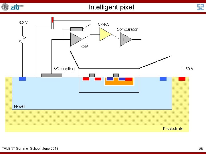
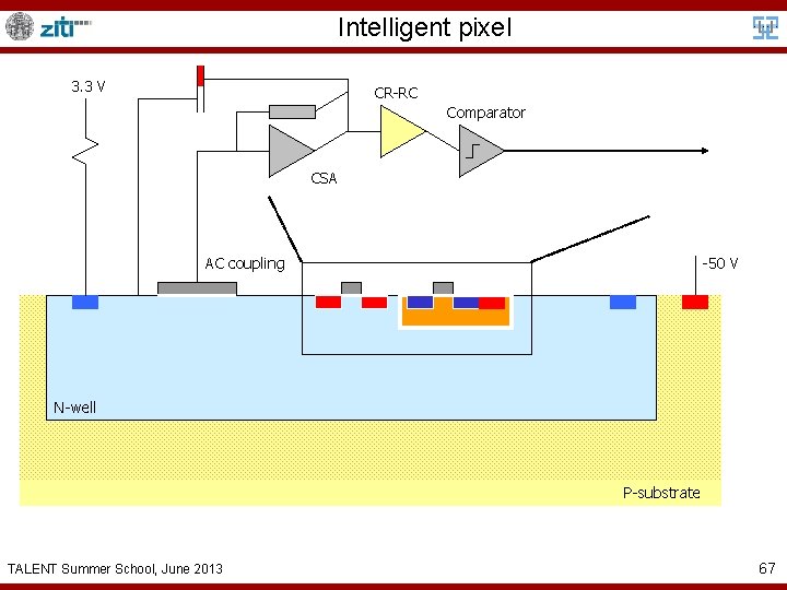
Intelligent pixel 3. 3 V CR-RC Comparator CSA AC coupling -50 V N-well P-substrate TALENT Summer School, June 2013 61

Intelligent pixel 3. 3 V CR-RC Comparator CSA AC coupling -50 V N-well P-substrate TALENT Summer School, June 2013 62

Intelligent pixel 3. 3 V CR-RC Comparator CSA AC coupling -50 V N-well P-substrate TALENT Summer School, June 2013 63

Intelligent pixel 3. 3 V CR-RC Comparator CSA AC coupling -50 V N-well P-substrate TALENT Summer School, June 2013 64

Intelligent pixel 3. 3 V CR-RC Comparator CSA AC coupling -50 V N-well P-substrate TALENT Summer School, June 2013 65

Intelligent pixel 3. 3 V CR-RC Comparator CSA AC coupling -50 V N-well P-substrate TALENT Summer School, June 2013 66

Intelligent pixel 3. 3 V CR-RC Comparator CSA AC coupling -50 V N-well P-substrate TALENT Summer School, June 2013 67

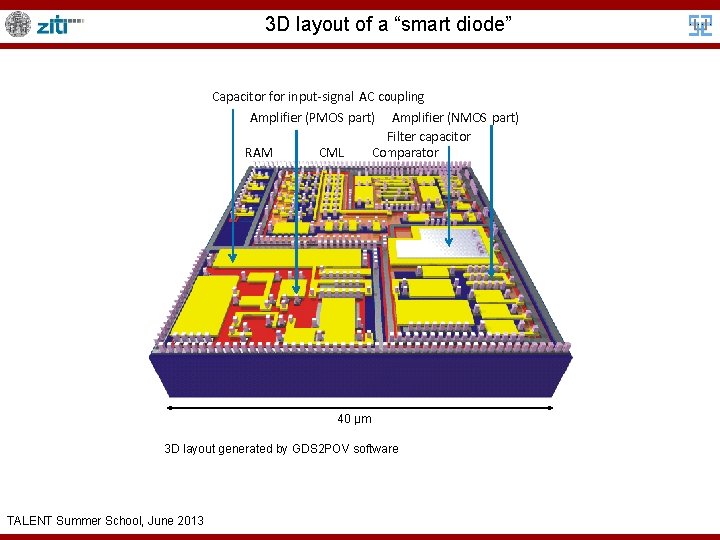
3 D layout of a “smart diode” 40 µm 3 D layout generated by GDS 2 POV software TALENT Summer School, June 2013

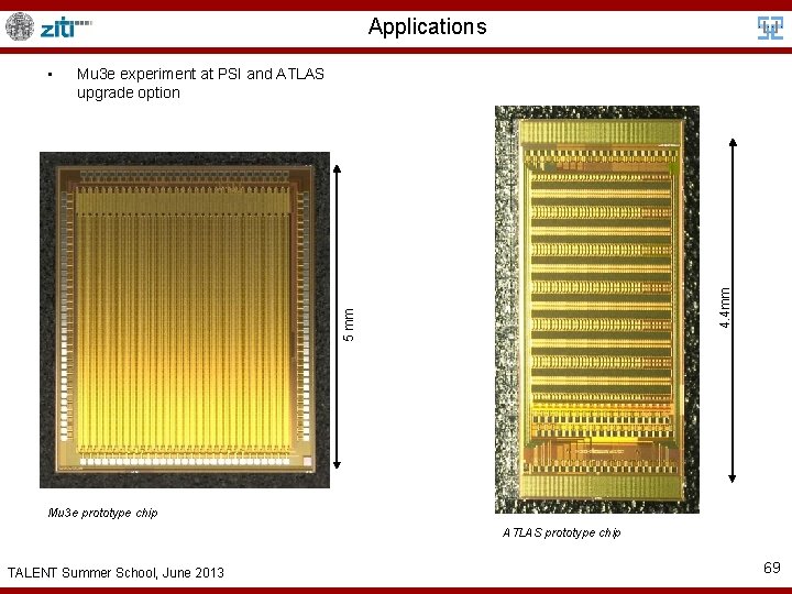
Applications 4. 4 mm Mu 3 e experiment at PSI and ATLAS upgrade option 5 mm • Mu 3 e prototype chip ATLAS prototype chip TALENT Summer School, June 2013 69

TWELL - MAPS TALENT Summer School, June 2013 70

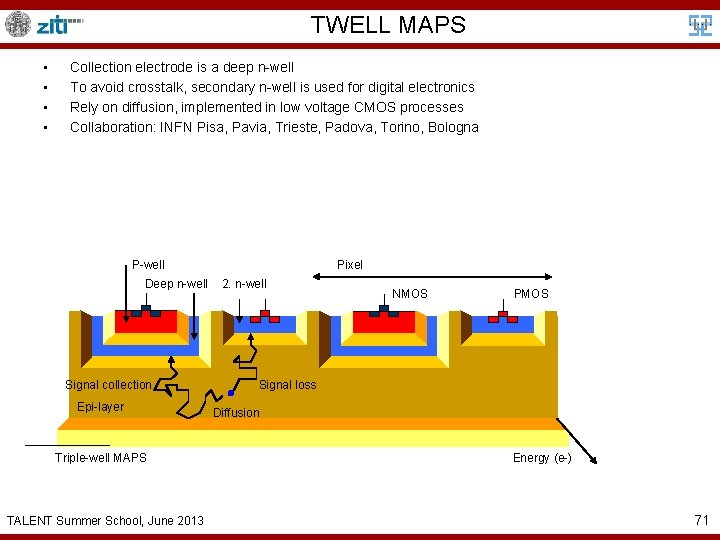
TWELL MAPS • • Collection electrode is a deep n-well To avoid crosstalk, secondary n-well is used for digital electronics Rely on diffusion, implemented in low voltage CMOS processes Collaboration: INFN Pisa, Pavia, Trieste, Padova, Torino, Bologna P-well Deep n-well Signal collection Epi-layer Triple-well MAPS TALENT Summer School, June 2013 Pixel 2. n-well NMOS PMOS Signal loss Diffusion Energy (e-) 71

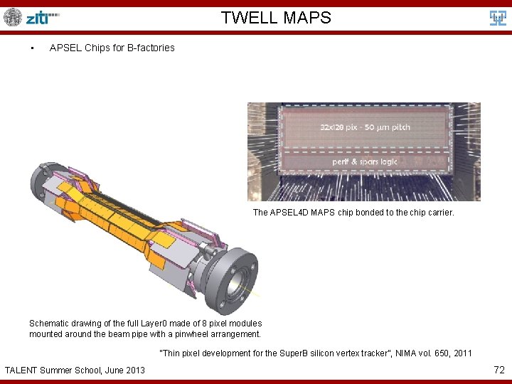
TWELL MAPS • APSEL Chips for B-factories The APSEL 4 D MAPS chip bonded to the chip carrier. Schematic drawing of the full Layer 0 made of 8 pixel modules mounted around the beam pipe with a pinwheel arrangement. “Thin pixel development for the Super. B silicon vertex tracker”, NIMA vol. 650, 2011 TALENT Summer School, June 2013 72

Special monolithic technologies TALENT Summer School, June 2013 73

SOI TALENT Summer School, June 2013 74

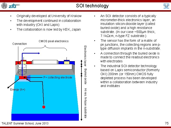
SOI technology • • Originally developed at University of Krakow The development continued in collaboration with industry (OKI and Lapis) The collaboration is now led by KEK, Japan Connection • CMOS pixel electronics TALENT Summer School, June 2013 • Hi res. N-type substrate Energy (h+) Electronics layer Buried oxide P+ collecting electrode • An SOI detector consists of a typically micrometer-thick electronics layer, an insulation silicon-dioxide layer (called buried oxide) and a high resistance substrate. (In our case ~500 m thick, 7. 1 k cm, n-type FZ substrate. ) The sensor has the form of a matrix of pn junctions, the collecting regions are ptype diffusion implants in the n-substrate. A connection through the buried oxide is made to connect the readout electronics with electrodes The industrial SOI detector technology based on Lapis semiconductor (formerly OKI) 200 nm (or 150 nm) CMOS fully depleted process has been developed within a collaboration between industry and institutes 75

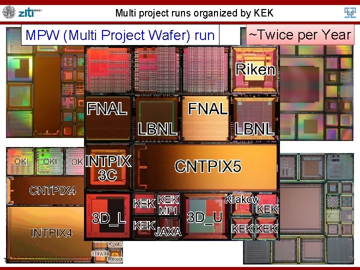
Multi project runs organized by KEK MPW (Multi Project Wafer) run TALENT Summer School, June 2013 ~Twice per Year 76

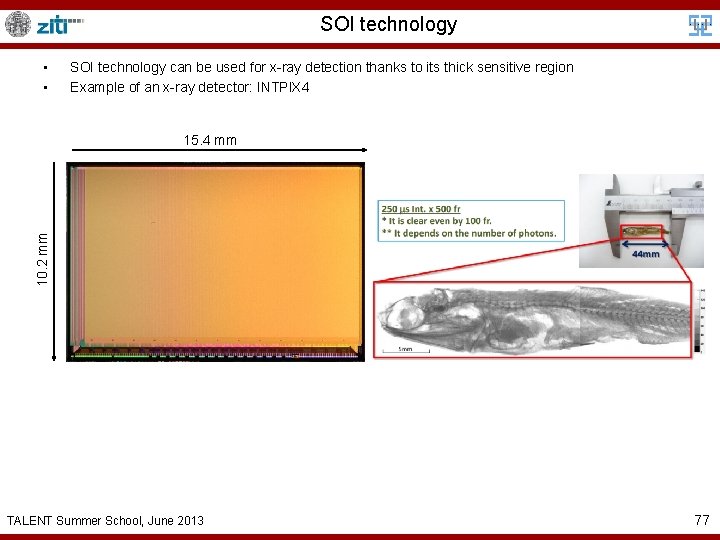
SOI technology • • SOI technology can be used for x-ray detection thanks to its thick sensitive region Example of an x-ray detector: INTPIX 4 10. 2 mm 15. 4 mm TALENT Summer School, June 2013 77

DEPFET TALENT Summer School, June 2013 78

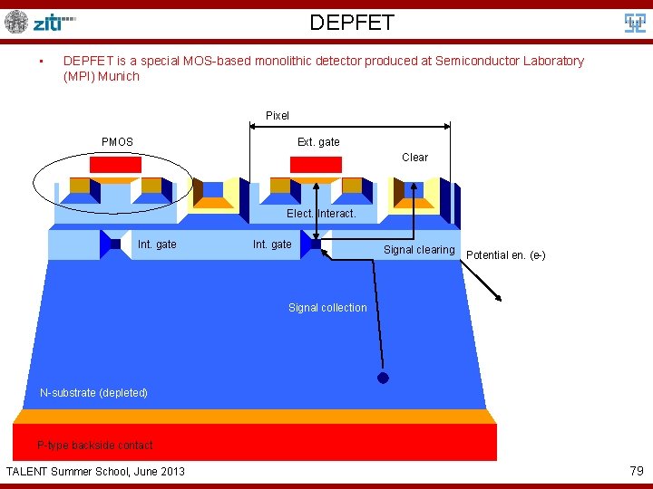
DEPFET • DEPFET is a special MOS-based monolithic detector produced at Semiconductor Laboratory (MPI) Munich Pixel PMOS Ext. gate Clear Elect. Interact. Int. gate Signal clearing Potential en. (e-) Signal collection N-substrate (depleted) P-type backside contact TALENT Summer School, June 2013 79

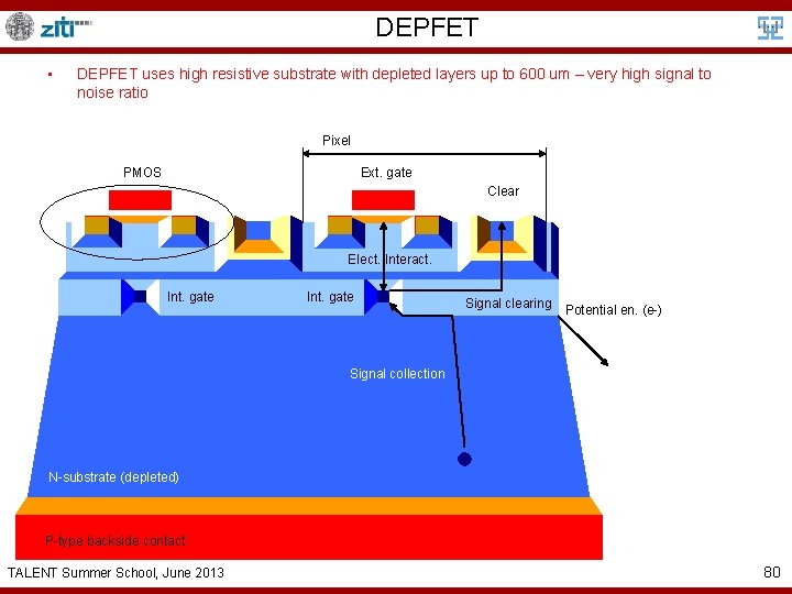
DEPFET • DEPFET uses high resistive substrate with depleted layers up to 600 um – very high signal to noise ratio Pixel PMOS Ext. gate Clear Elect. Interact. Int. gate Signal clearing Potential en. (e-) Signal collection N-substrate (depleted) P-type backside contact TALENT Summer School, June 2013 80

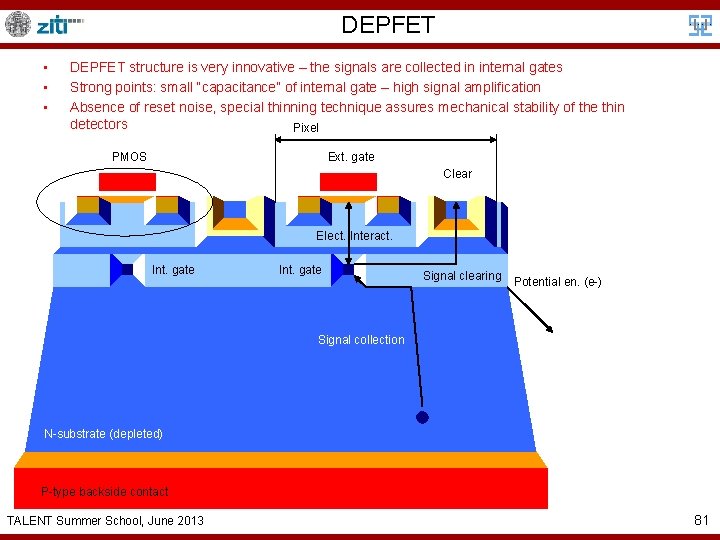
DEPFET • • • DEPFET structure is very innovative – the signals are collected in internal gates Strong points: small “capacitance” of internal gate – high signal amplification Absence of reset noise, special thinning technique assures mechanical stability of the thin detectors Pixel PMOS Ext. gate Clear Elect. Interact. Int. gate Signal clearing Potential en. (e-) Signal collection N-substrate (depleted) P-type backside contact TALENT Summer School, June 2013 81

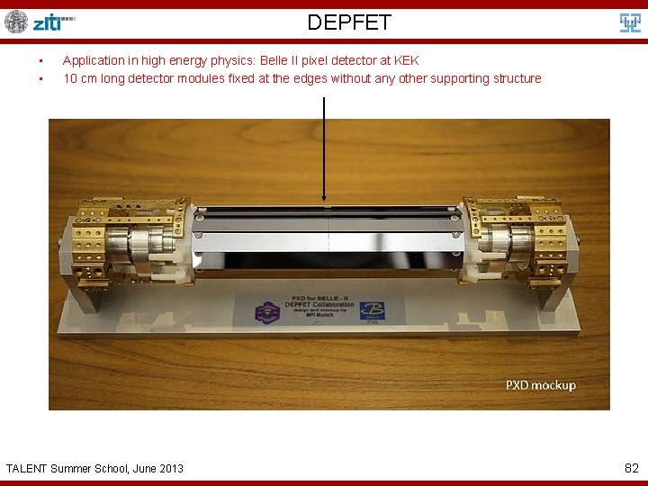
DEPFET • • Application in high energy physics: Belle II pixel detector at KEK 10 cm long detector modules fixed at the edges without any other supporting structure TALENT Summer School, June 2013 82

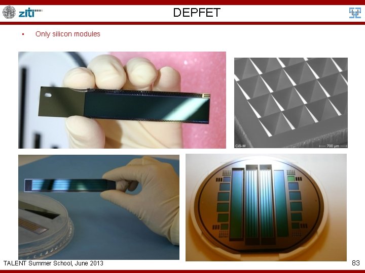
DEPFET • Only silicon modules TALENT Summer School, June 2013 83

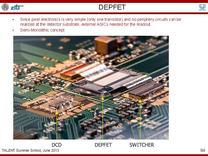
DEPFET • • Since pixel electronics is very simple (only one transistor) and no periphery circuits can be realized at the detector substrate, external ASICs needed for the readout Semi-Monolithic concept TALENT Summer School, June 2013 84

• Thank you! TALENT Summer School, June 2013 85