Monolithic Pixel Sensors in a Quadruple Well CMOS

- Slides: 15

Monolithic Pixel Sensors in a Quadruple Well CMOS Technology S. Zucca PRIN-VIPIX-Super. B Collaboration meeting – 27 th March, 2013 - Milano

Outline Motivation: design of high granularity monolithic active pixel sensors (MAPS) for application to the Layer 0 of the Super. B SVT Low material budget (<1% X 0) Pixel pitch of 50 μm in both x and y directions High hit rate (100 MHz/cm 2) & fast timestamp (< 1μs) - challenging for CMOS MAPS High radiation hardness (3 Mrad/yr and 5∙ 1012 1 Me. V neutron equivalent/cm 2/yr) – challenging for CMOS MAPS Apsel 4 well front-end readout Analog FE and charge collection performance Effects of neutron irradiation on charge collection properties Monte Carlo charge loss model Ongoing activities and future plans

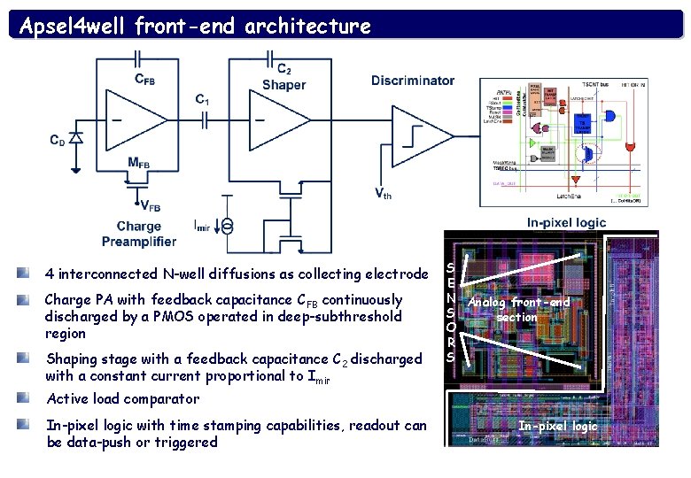
Apsel 4 well front-end architecture 4 interconnected N-well diffusions as collecting electrode Charge PA with feedback capacitance CFB continuously discharged by a PMOS operated in deep-subthreshold region Shaping stage with a feedback capacitance C 2 discharged with a constant current proportional to Imir S E N Analog front-end S section O R S Active load comparator In-pixel logic with time stamping capabilities, readout can be data-push or triggered In-pixel logic

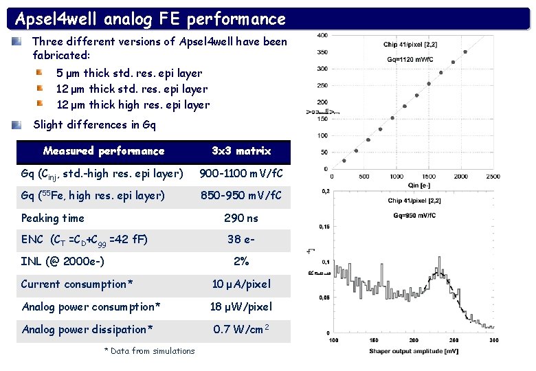
Apsel 4 well analog FE performance Three different versions of Apsel 4 well have been fabricated: 5 μm thick std. res. epi layer 12 μm thick high res. epi layer Slight differences in Gq Measured performance 3 x 3 matrix Gq (Cinj, std. -high res. epi layer) 900 -1100 m. V/f. C Gq (55 Fe, high res. epi layer) 850 -950 m. V/f. C Peaking time 290 ns ENC (CT =CD+Cgg =42 f. F) INL (@ 2000 e-) 38 e 2% Current consumption* 10 μA/pixel Analog power consumption* 18 μW/pixel Analog power dissipation* * Data from simulations 0. 7 W/cm 2 4

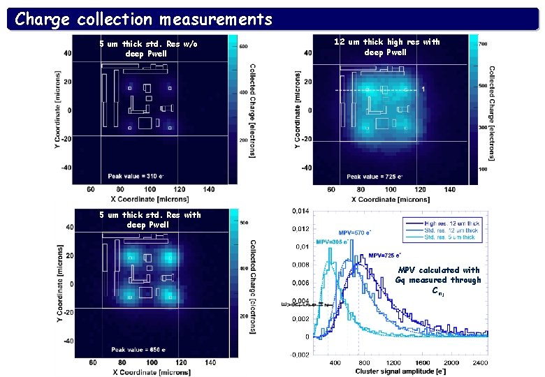
Charge collection measurements 5 um thick std. Res w/o deep Pwell 12 um thick high res with deep Pwell 5 um thick std. Res with deep Pwell MPV calculated with Gq measured through Cinj

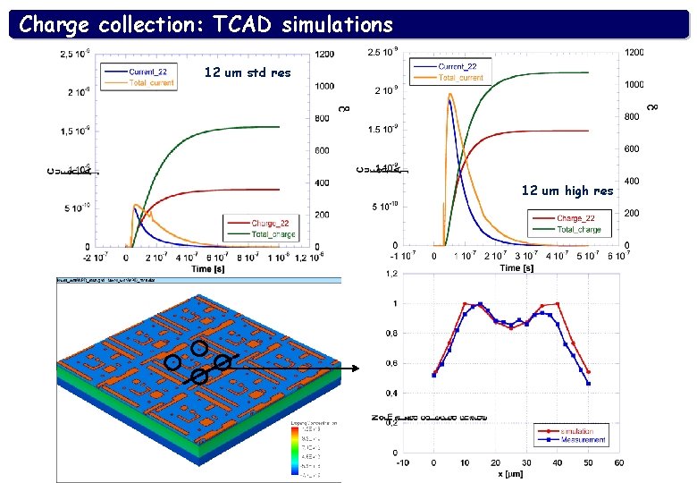
Charge collection: TCAD simulations 12 um std res 12 um high res

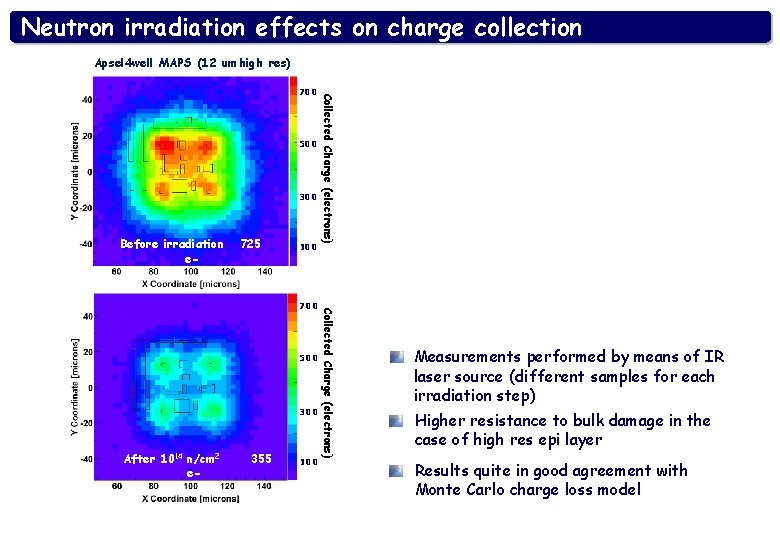
Neutron irradiation effects on charge collection Apsel 4 well MAPS (12 um high res) 500 300 Before irradiation e- 725 100 500 300 After 1014 n/cm 2 e- 355 100 Collected Charge (electrons) 700 Measurements performed by means of IR laser source (different samples for each irradiation step) Higher resistance to bulk damage in the case of high res epi layer Results quite in good agreement with Monte Carlo charge loss model

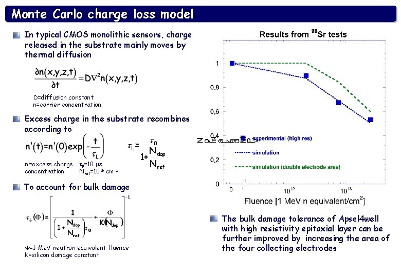
Monte Carlo charge loss model In typical CMOS monolithic sensors, charge released in the substrate mainly moves by thermal diffusion D=diffusion constant n=carrier concentration Excess charge in the substrate recombines according to n’=excess charge t 0=10 ms concentration Nref=1016 cm-3 To account for bulk damage F=1 -Me. V-neutron equivalent fluence K=silicon damage constant The bulk damage tolerance of Apsel 4 well with high resistivity epitaxial layer can be further improved by increasing the area of the four collecting electrodes

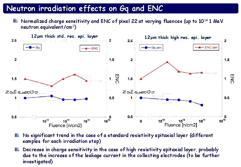
Neutron irradiation effects on Gq and ENC Normalized charge sensitivity and ENC of pixel 22 at varying fluences (up to 10 14 1 Me. V neutron equivalent/cm 2) 12 μm thick std. res. epi. layer 12 μm thick high res. epi. layer No significant trend in the case of a standard resistivity epitaxial layer (different samples for each irradiation step) Decrease in charge sensitivity in the case of high resistivity epitaxial layer, probably due to the increase of the leakage current in the collecting electrodes (to be further investigated)

Ongoing activities and future plans Irradiation with γ-rays has started and devices are under test after the first step (1 Mrad) Tests of “immunity” to substrate noise phenomena Optimization of 3 D TCAD simulations for: Improving the precision of the Monte Carlo simulation results by further investigating the dependence of the depleted volume on the collecting electrode area Evaluating the depleted volume as a function of the inverse biasing voltage Future plans Tests on back thinned (down to 50 μm and 25 μm) Apsel 4 well samples featuring a 12 μm thick high res epi layer

Backup slides

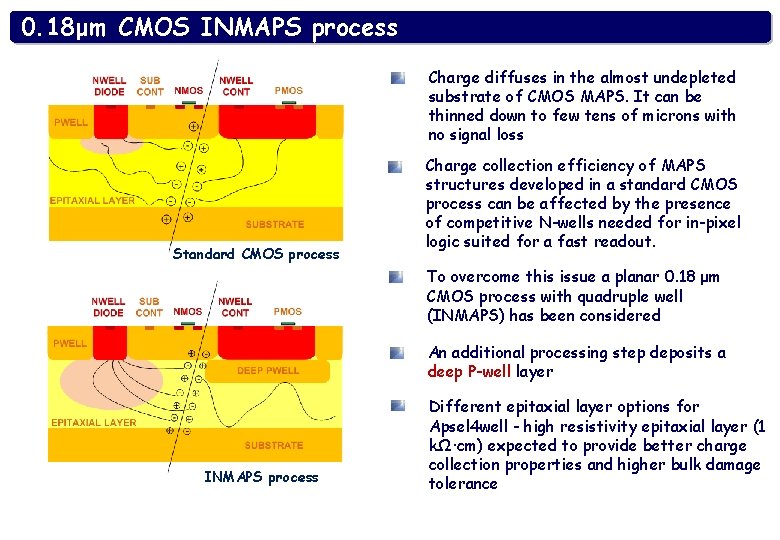
0. 18 μm CMOS INMAPS process Charge diffuses in the almost undepleted substrate of CMOS MAPS. It can be thinned down to few tens of microns with no signal loss Standard CMOS process Charge collection efficiency of MAPS structures developed in a standard CMOS process can be affected by the presence of competitive N-wells needed for in-pixel logic suited for a fast readout. To overcome this issue a planar 0. 18 μm CMOS process with quadruple well (INMAPS) has been considered An additional processing step deposits a deep P-well layer INMAPS process Different epitaxial layer options for Apsel 4 well - high resistivity epitaxial layer (1 kΩ∙cm) expected to provide better charge collection properties and higher bulk damage tolerance

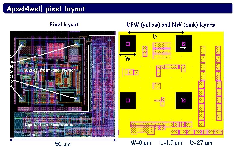
Apsel 4 well pixel layout Pixel layout DPW (yellow) and NW (pink) layers D S E N S O R S L W Analog front-end section Digital front-end section 50 μm W=8 μm L=1. 5 μm D=27 μm

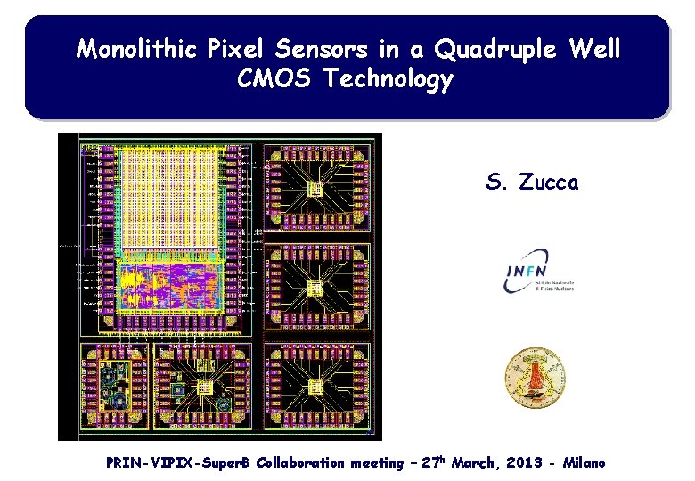
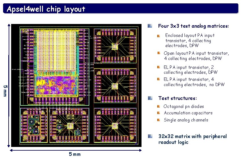
Apsel 4 well chip layout Four 3 x 3 test analog matrices: Enclosed layout PA input transistor, 4 collecting electrodes, DPW Open layout PA input transistor, 4 collecting electrodes, DPW EL PA input transistor, 2 collecting electrodes, DPW 5 mm EL PA input transistor, 4 collecting electrodes, no DPW Test structures: Octagonal pn diodes Accumulation capacitors Single analog channels 32 x 32 matrix with peripheral readout logic 5 mm

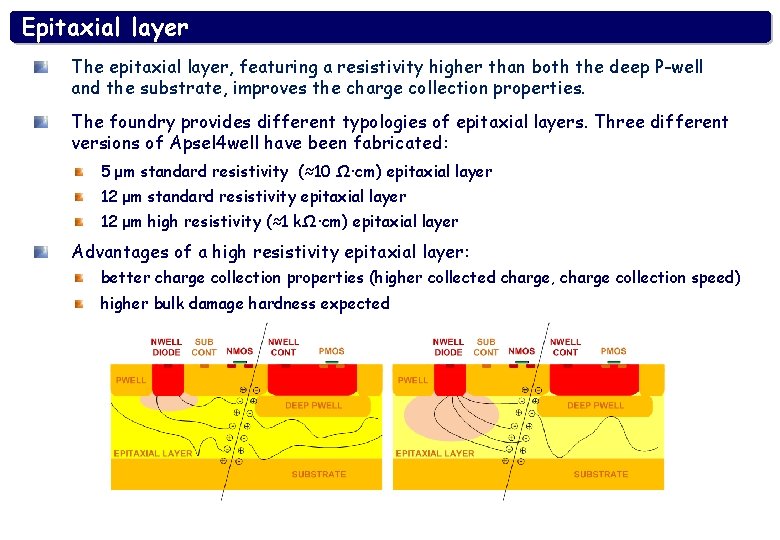
Epitaxial layer The epitaxial layer, featuring a resistivity higher than both the deep P-well and the substrate, improves the charge collection properties. The foundry provides different typologies of epitaxial layers. Three different versions of Apsel 4 well have been fabricated: 5 μm standard resistivity (≈10 Ω∙cm) epitaxial layer 12 μm standard resistivity epitaxial layer 12 μm high resistivity (≈1 kΩ∙cm) epitaxial layer Advantages of a high resistivity epitaxial layer: better charge collection properties (higher collected charge, charge collection speed) higher bulk damage hardness expected