Adapting CMOS Active Pixel Sensors for Hg Cd


- Slides: 20

Adapting CMOS Active Pixel Sensors for Hg. Cd. Te Photodiodes Zeynep Dilli, Neil Goldsman, Martin Peckerar, Nibir Dhar

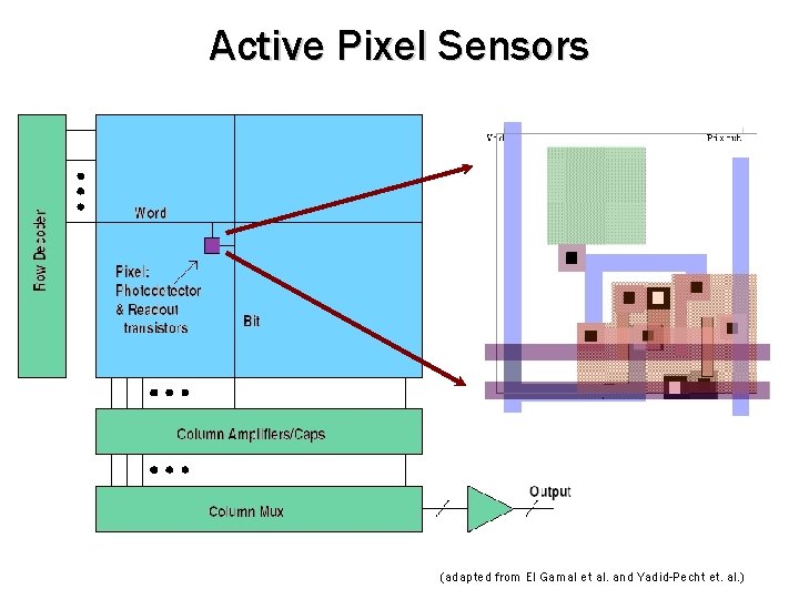
Active Pixel Sensors (adapted from El Gamal et al. and Yadid-Pecht et. al. )

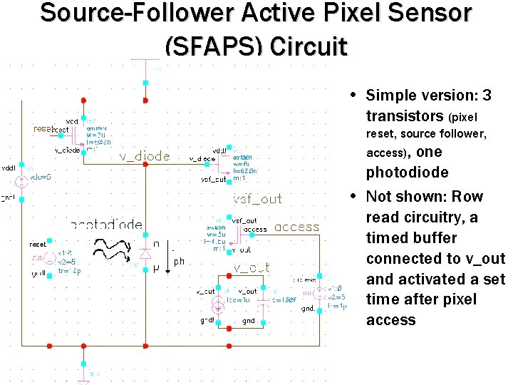
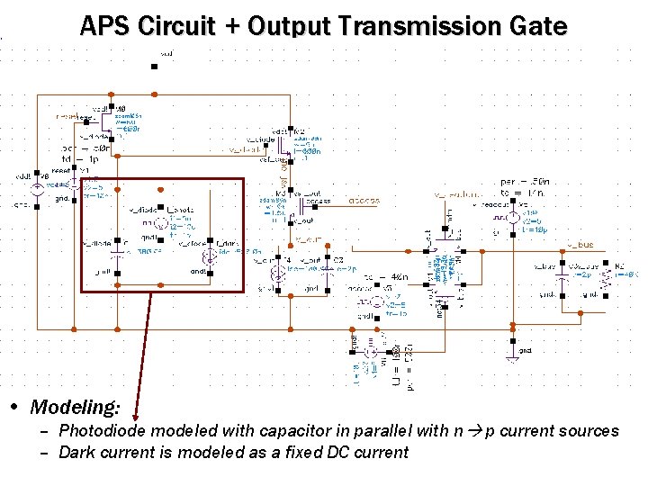
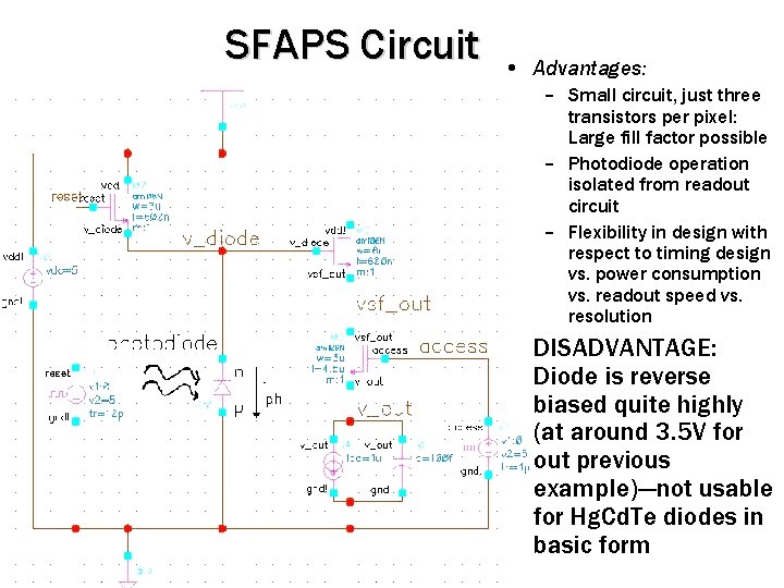
Source-Follower Active Pixel Sensor (SFAPS) Circuit • Simple version: 3 transistors (pixel reset, source follower, access), one photodiode • Not shown: Row read circuitry, a timed buffer connected to v_out and activated a set time after pixel access

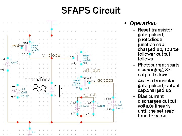
SFAPS Circuit • Operation: – Reset transistor gate pulsed, photodiode junction cap. charged up, source follower output follows – Photocurrent starts discharging, SF output follows – Access transistor gate pulsed, output cap. charged up – Bias current discharges output voltage linearly until the set read time for v_out

SFAPS Circuit • Operation: – Reset transistor gate pulsed, photodiode junction cap. charged up, source follower output follows – Photocurrent starts discharging, SF output follows – Access transistor gate pulsed, output cap. charged up – Bias current discharges output voltage linearly until the set read time for v_out

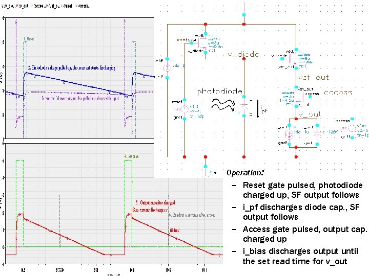
• Operation: – Reset gate pulsed, photodiode charged up, SF output follows – i_pf discharges diode cap. , SF output follows – Access gate pulsed, output cap. charged up – i_bias discharges output until the set read time for v_out

APS Circuit + Output Transmission Gate • Modeling: – Photodiode modeled with capacitor in parallel with n p current sources – Dark current is modeled as a fixed DC current

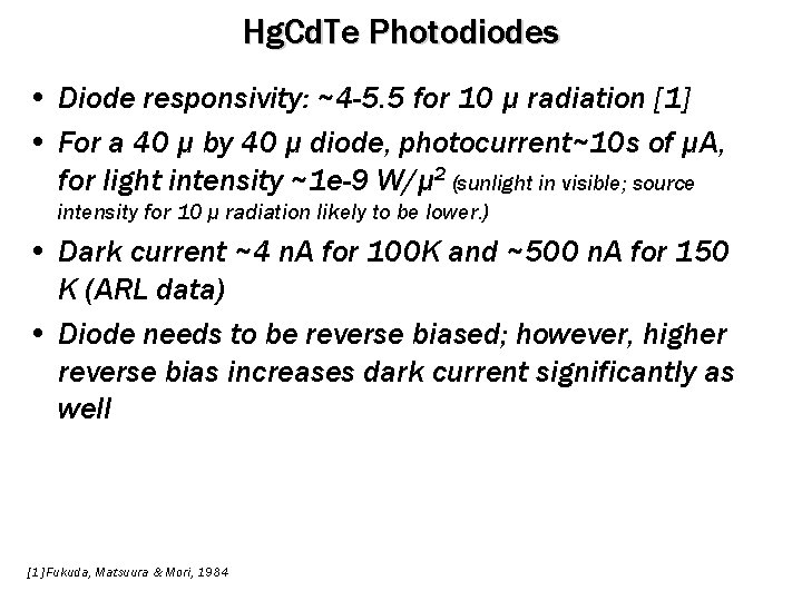
Hg. Cd. Te Photodiodes • Diode responsivity: ~4 -5. 5 for 10 μ radiation [1] • For a 40 μ by 40 μ diode, photocurrent~10 s of μA, for light intensity ~1 e-9 W/μ 2 (sunlight in visible; source intensity for 10 μ radiation likely to be lower. ) • Dark current ~4 n. A for 100 K and ~500 n. A for 150 K (ARL data) • Diode needs to be reverse biased; however, higher reverse bias increases dark current significantly as well [1] Fukuda, Matsuura & Mori, 1984

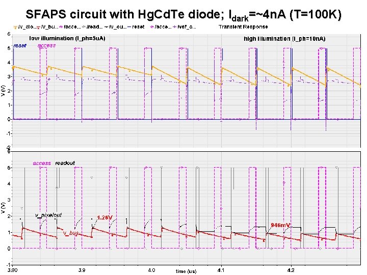
SFAPS circuit with Hg. Cd. Te diode; Idark=~4 n. A (T=100 K)

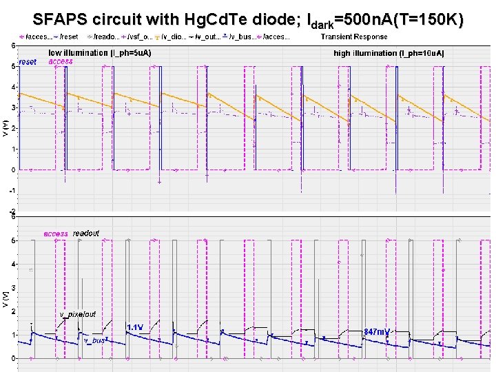
SFAPS circuit with Hg. Cd. Te diode; Idark=500 n. A(T=150 K)

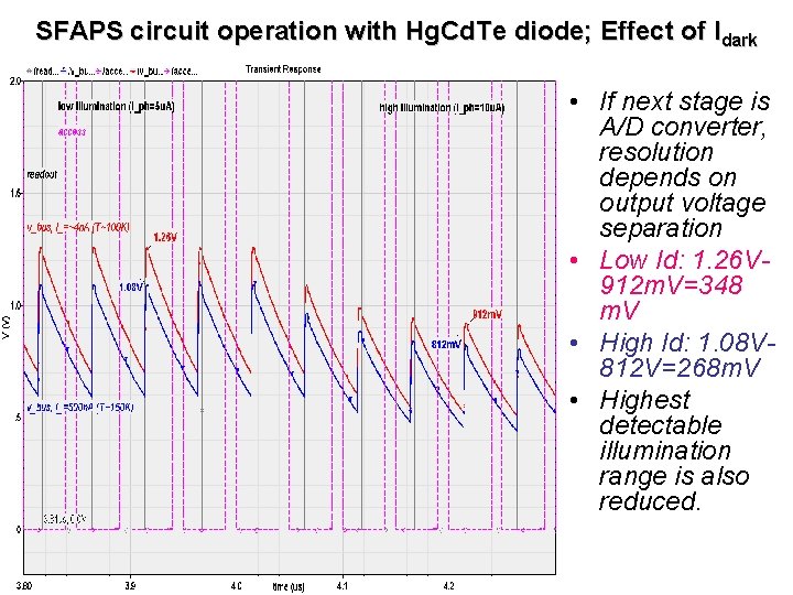
SFAPS circuit operation with Hg. Cd. Te diode; Effect of Idark • If next stage is A/D converter, resolution depends on output voltage separation • Low Id: 1. 26 V 912 m. V=348 m. V • High Id: 1. 08 V 812 V=268 m. V • Highest detectable illumination range is also reduced.

SFAPS Circuit • Advantages: – Small circuit, just three transistors per pixel: Large fill factor possible – Photodiode operation isolated from readout circuit – Flexibility in design with respect to timing design vs. power consumption vs. readout speed vs. resolution • DISADVANTAGE: Diode is reverse biased quite highly (at around 3. 5 V for out previous example)---not usable for Hg. Cd. Te diodes in basic form

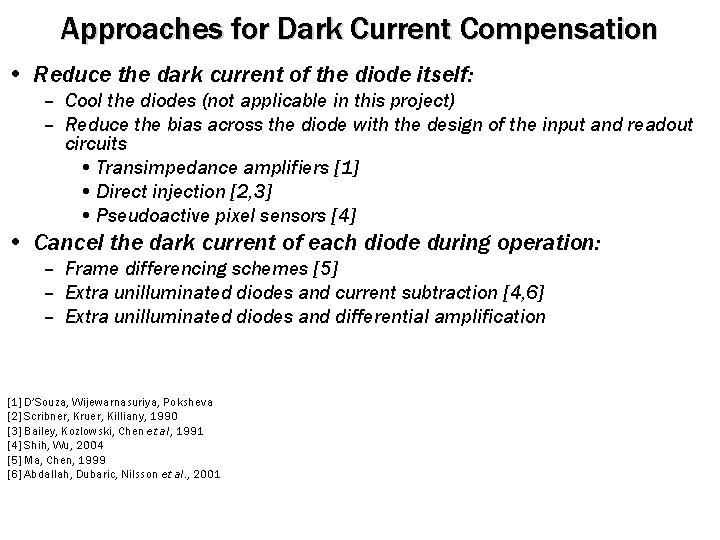
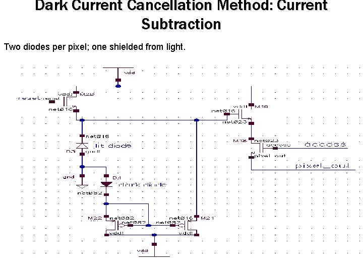
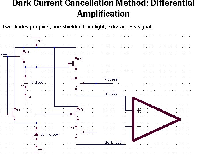
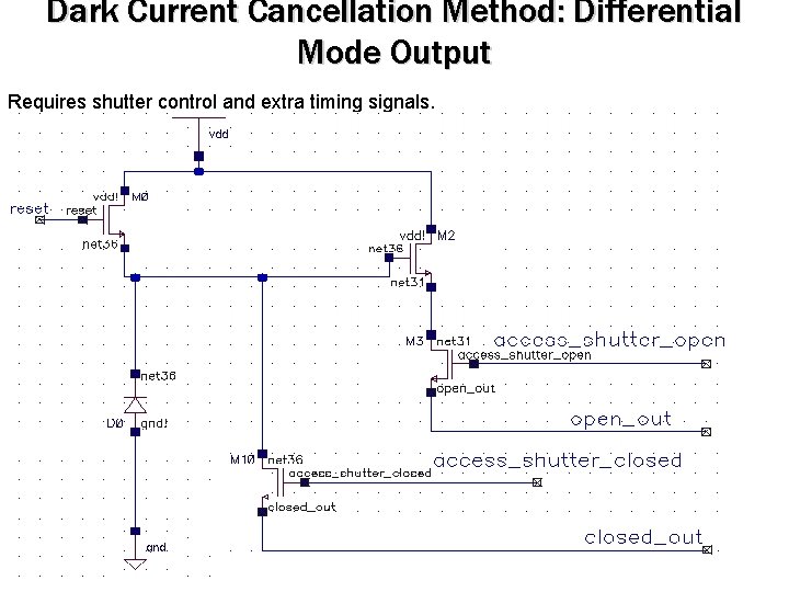
Approaches for Dark Current Compensation • Reduce the dark current of the diode itself: – Cool the diodes (not applicable in this project) – Reduce the bias across the diode with the design of the input and readout circuits • Transimpedance amplifiers [1] • Direct injection [2, 3] • Pseudoactive pixel sensors [4] • Cancel the dark current of each diode during operation: – Frame differencing schemes [5] – Extra unilluminated diodes and current subtraction [4, 6] – Extra unilluminated diodes and differential amplification [1] D’Souza, Wijewarnasuriya, Poksheva [2] Scribner, Kruer, Killiany, 1990 [3] Bailey, Kozlowski, Chen et al, 1991 [4] Shih, Wu, 2004 [5] Ma, Chen, 1999 [6] Abdallah, Dubaric, Nilsson et al. , 2001

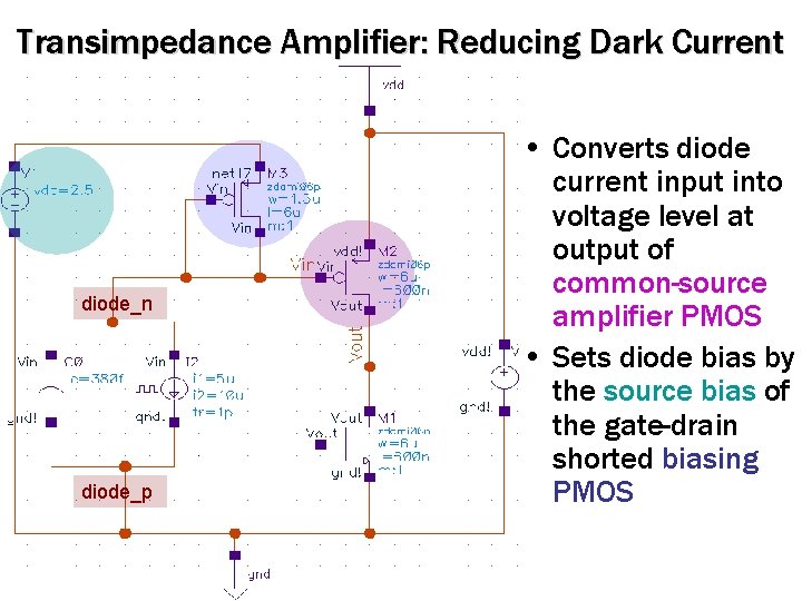
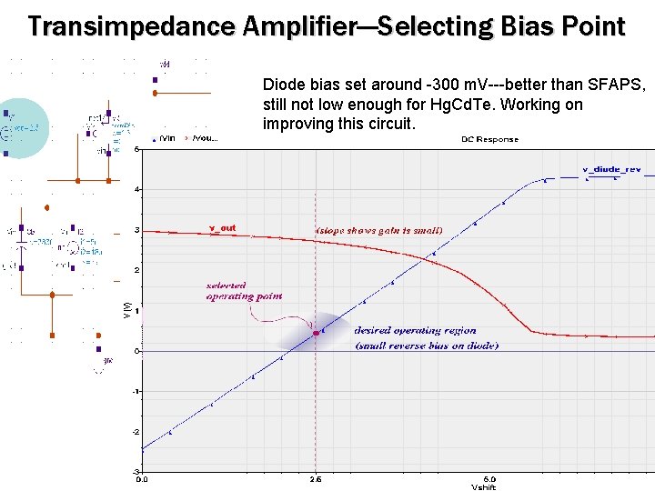
Transimpedance Amplifier: Reducing Dark Current diode_n diode_p • Converts diode current input into voltage level at output of common-source amplifier PMOS • Sets diode bias by the source bias of the gate-drain shorted biasing PMOS

Transimpedance Amplifier---Selecting Bias Point Diode bias set around -300 m. V---better than SFAPS, still not low enough for Hg. Cd. Te. Working on improving this circuit.

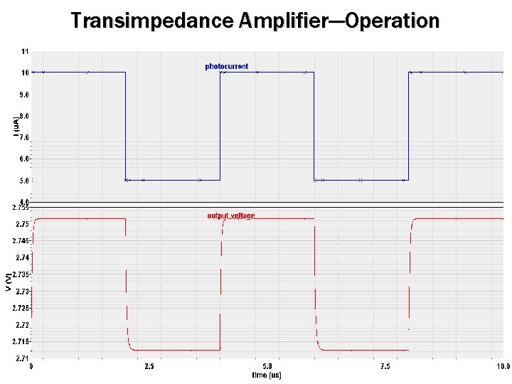
Transimpedance Amplifier---Operation

Dark Current Cancellation Method: Current Subtraction Two diodes per pixel; one shielded from light.

Dark Current Cancellation Method: Differential Amplification Two diodes per pixel; one shielded from light; extra access signal.

Dark Current Cancellation Method: Differential Mode Output Requires shutter control and extra timing signals.

Future Work • Investigate – – Transimpedance amplifiers (further) Direct injection circuits Different biasing schemes Unilluminated extra pixels and dark current cancellation • Consider – Hg. Cd. Te requirement: Very low reverse bias – Hybrid integration [1] allows more space for readout circuitry per pixel; still, optimize circuits for power consumption – Timing requirements and tradeoffs? (Extrapolate from SFAPS work) – Sensitivity requirements and tradeoffs? (Extrapolate from SFAPS work) [1] Bailey, Kozlowski, Chen et. al. , 1991 and later work