The Memory Controller Overview ControlAddress Lines usage Memory
![Static Memory Controller OE* Output Enable SRAM Memory Devices WE* Write Enable BE[3: 0]* Static Memory Controller OE* Output Enable SRAM Memory Devices WE* Write Enable BE[3: 0]*](https://slidetodoc.com/presentation_image_h/02cac1483ef128f463ab4d294f49d904/image-24.jpg)
- Slides: 26

The Memory Controller Overview Control/Address Lines usage Memory Module Configuration Register settings Chip Select Base Address Register settings Device considerations

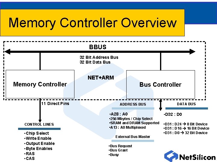
Memory Controller Overview BBUS 32 Bit Address Bus 32 Bit Data Bus NET+ARM Memory Controller 11 Direct Pins Bus Controller ADDRESS BUS • A 28 : A 0 CONTROL LINES • Chip Select • Write Enable • Output Enable • Byte Enables • RAS • CAS • 256 Mbytes / Chip Select • SRAM and DRAM Supported • A 13 : A 0 Multiplexed External Bus Master • Bus Request • Bus Grant • Busy DATA BUS • D 32 : D 0 • D 31 : D 24 8 Bit Device • D 31 : D 16 Bit Device • D 31 : D 0 32 Bit Device

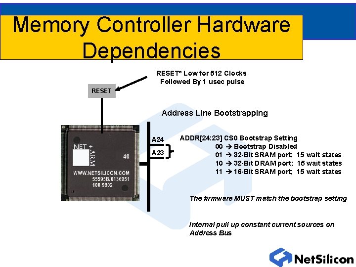
Memory Controller Hardware Dependencies RESET* Low for 512 Clocks Followed By 1 usec pulse RESET Address Line Bootstrapping A 24 A 23 ADDR[24: 23] CS 0 Bootstrap Setting 00 Bootstrap Disabled 01 32 -Bit SRAM port; 15 wait states 10 32 -Bit DRAM port; 15 wait states 11 16 -Bit SRAM port; 15 wait states The firmware MUST match the bootstrap setting Internal pull up constant current sources on Address Bus

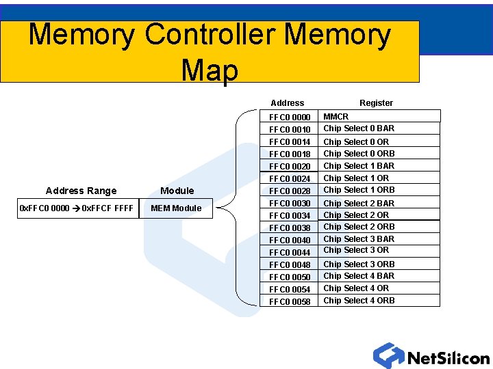
Memory Controller Memory Map Address FFC 0 0000 FFC 0 0014 FFC 0 0018 FFC 0 0020 FFC 0 0024 Address Range 0 x. FFC 0 0000 0 x. FFCF FFFF Module MEM Module FFC 0 0028 FFC 0 0030 FFC 0 0034 FFC 0 0038 FFC 0 0040 FFC 0 0044 FFC 0 0048 FFC 0 0050 FFC 0 0054 FFC 0 0058 Register MMCR Chip Select 0 BAR Chip Select 0 ORB Chip Select 1 BAR Chip Select 1 ORB Chip Select 2 BAR Chip Select 2 ORB Chip Select 3 BAR Chip Select 3 ORB Chip Select 4 BAR Chip Select 4 ORB

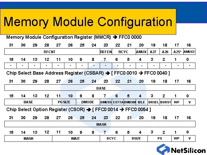
Memory Module Configuration Register (MMCR) FFC 0 0000 31 30 29 28 27 26 25 24 RFCNT 15 - 14 - 13 - 12 - 23 22 RCYC REFEN 11 - 10 - 9 - 8 - 7 - 21 6 - 5 - 20 19 18 17 16 AMUX A 27 A 26 A 25* AMUX 2 4 - 3 - 2 - 1 0 - - Chip Select Base Address Register (CSBAR) [ FFC 0 0010 FFC 0 0040 ] 31 30 29 28 27 26 25 24 23 22 21 20 19 18 17 16 6 5 4 3 2 1 0 BASE 15 14 13 12 BASE 11 10 9 PGSIZE 8 DMODE 7 DMUXS EXTTA DMUXM IDLE DRSEL BURST WP V Chip Select Option Register (CSOR) [ FFC 0 0014 FFC 0 0054 ] 31 30 29 28 27 26 25 24 23 22 21 20 19 18 17 16 6 5 4 3 2 1 0 MASK 15 14 13 MASK 12 11 10 9 WAIT 8 7 BCYC BSIZE PS WP V

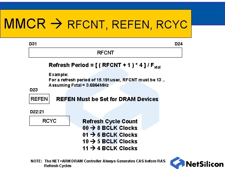
MMCR RFCNT, REFEN, RCYC D 24 D 31 RFCNT Refresh Period = [ ( RFCNT + 1 ) * 4 ] / Fxtal Example: For a refresh period of 15. 191 usec, RFCNT must be 13. . Assuming Fxtal = 3. 6864 MHz D 23 REFEN Must be Set for DRAM Devices D 22: 21 RCYC Refresh Cycle Count 00 8 BCLK Clocks 01 6 BCLK Clocks 10 5 BCLK Clocks 11 4 BCLK Clocks NOTE: The NET+ARM DRAM Controller Always Generates CAS before RAS Refresh Cycles

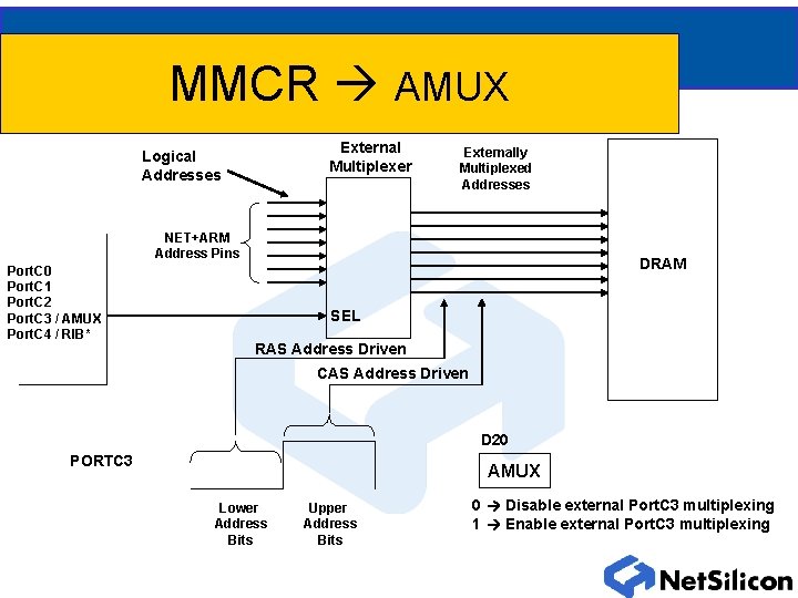
MMCR AMUX External Multiplexer Logical Addresses Externally Multiplexed Addresses NET+ARM Address Pins Port. C 0 Port. C 1 Port. C 2 Port. C 3 / AMUX Port. C 4 / RIB* DRAM SEL RAS Address Driven CAS Address Driven D 20 PORTC 3 AMUX Lower Address Bits Upper Address Bits 0 Disable external Port. C 3 multiplexing 1 Enable external Port. C 3 multiplexing

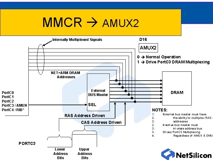
MMCR AMUX 2 Internally Multiplexed Signals D 16 AMUX 2 0 Normal Operation 1 Drive Port. C 3 DRAM Multiplexing NET+ARM DRAM Addresses External BUS Master Port. C 0 Port. C 1 Port. C 2 Port. C 3 / AMUX Port. C 4 / RIB* DRAM SEL NOTES: RAS Address Driven CAS Address Driven PORTC 3 Lower Address Bits Upper Address Bits 1. 2. 3. 3. 4. External bus master must have the ability to multiplex RAS & addresses Inactive bus master must tri-state address bus Drives Port. C 3 Multiplexing Regardless of AMUX & DMUX

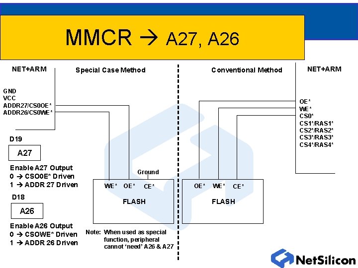
MMCR A 27, A 26 NET+ARM Conventional Method Special Case Method GND VCC ADDR 27/CS 0 OE* ADDR 26/CS 0 WE* OE* WE* CS 0* CS 1*/RAS 1* CS 2*/RAS 2* CS 3*/RAS 3* CS 4*/RAS 4* D 19 A 27 Enable A 27 Output 0 CSO 0 E* Driven 1 ADDR 27 Driven D 18 Ground WE* OE* CE* FLASH A 26 Enable A 26 Output 0 CSOWE* Driven 1 ADDR 26 Driven NET+ARM Note: When used as special function, peripheral cannot ‘need’ A 26 & A 27 OE* WE* CE* FLASH

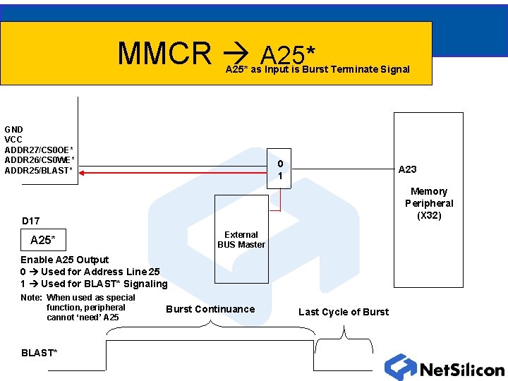
MMCR A 25* as Input is Burst Terminate Signal GND VCC ADDR 27/CS 0 OE* ADDR 26/CS 0 WE* ADDR 25/BLAST* 0 1 A 23 Memory Peripheral (X 32) D 17 External BUS Master A 25* Enable A 25 Output 0 Used for Address Line 25 1 Used for BLAST* Signaling Note: When used as special function, peripheral cannot ‘need’ A 25 BLAST* Burst Continuance Last Cycle of Burst

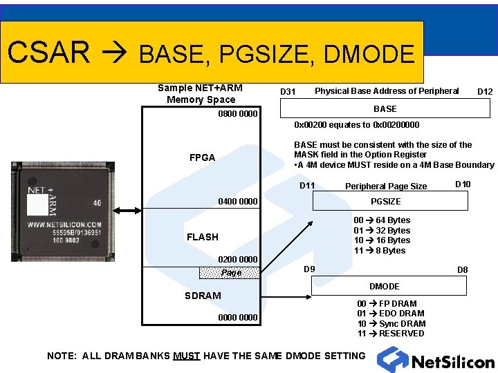
CSAR BASE, PGSIZE, DMODE Sample NET+ARM Memory Space Physical Base Address of Peripheral D 31 D 12 BASE 0800 0000 0 x 00200 equates to 0 x 00200000 BASE must be consistent with the size of the MASK field in the Option Register • A 4 M device MUST reside on a 4 M Base Boundary FPGA D 11 Peripheral Page Size 0400 0000 D 10 PGSIZE 00 64 Bytes 01 32 Bytes 10 16 Bytes 11 8 Bytes FLASH 0200 0000 Page SDRAM 0000 D 9 D 8 DMODE 00 FP DRAM 01 EDO DRAM 10 Sync DRAM 11 RESERVED NOTE: ALL DRAM BANKS MUST HAVE THE SAME DMODE SETTING

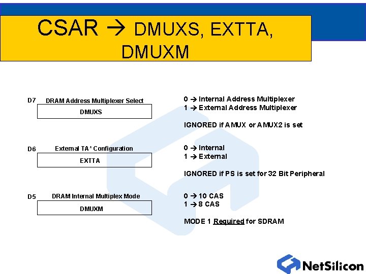
CSAR DMUXS, EXTTA, DMUXM D 7 DRAM Address Multiplexer Select DMUXS 0 Internal Address Multiplexer 1 External Address Multiplexer IGNORED if AMUX or AMUX 2 is set D 6 External TA* Configuration EXTTA 0 Internal 1 External IGNORED if PS is set for 32 Bit Peripheral D 5 DRAM Internal Multiplex Mode DMUXM 0 10 CAS 1 8 CAS MODE 1 Required for SDRAM

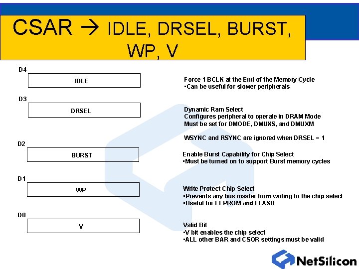
CSAR IDLE, DRSEL, BURST, WP, V D 4 IDLE Force 1 BCLK at the End of the Memory Cycle • Can be useful for slower peripherals D 3 DRSEL Dynamic Ram Select Configures peripheral to operate in DRAM Mode Must be set for DMODE, DMUXS, and DMUXM WSYNC and RSYNC are ignored when DRSEL = 1 D 2 BURST Enable Burst Capability for Chip Select • Must be turned on to support Burst memory cycles D 1 WP Write Protect Chip Select • Prevents any bus master from writing to the chip select • Useful for EEPROM and FLASH D 0 V Valid Bit • V bit enables the chip select • ALL other BAR and CSOR settings must be valid

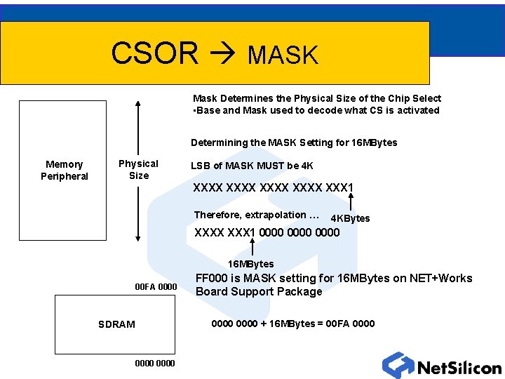
CSOR MASK Mask Determines the Physical Size of the Chip Select • Base and Mask used to decode what CS is activated Determining the MASK Setting for 16 MBytes Memory Peripheral Physical Size LSB of MASK MUST be 4 K XXXX XXX 1 Therefore, extrapolation … 4 KBytes XXXX 1 0000 16 MBytes 00 FA 0000 FF 000 is MASK setting for 16 MBytes on NET+Works Board Support Package 0000 + 16 MBytes = 00 FA 0000 SDRAM 0000

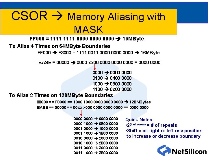
CSOR Memory Aliasing with MASK FF 000 = 1111 0000 16 MByte To Alias 4 Times on 64 MByte Boundaries FF 000 F 3000 = 1111 0000 16 MByte BASE = 00000 xx 00 0000 = 0000 0000 0100 0400 0000 1000 0800 0000 1100 0 c 00 0000 To Alias 8 Times on 128 MByte Boundaries 88000 == F 8000 == 1000 0000 128 MBytes BASE == 00000 == 00 xx x 0000 == 0000 0000 1000 0800 0001 0000 1000 0001 1000 1800 0010 0000 2000 0010 1000 2800 0011 0000 3000 0011 1000 3800 0000 Quick Notes: • 2(# of zeros) = # of repeats • Shift x bit right or left one position to increase or decrease boundary

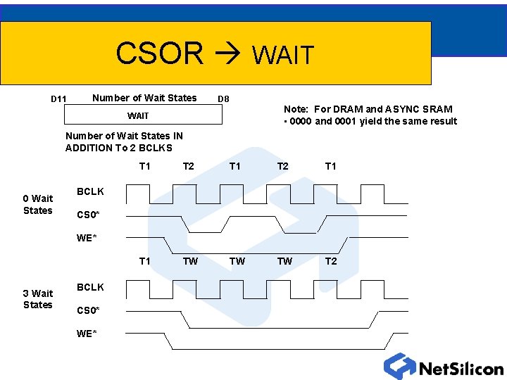
CSOR WAIT D 11 Number of Wait States D 8 Note: For DRAM and ASYNC SRAM • 0000 and 0001 yield the same result WAIT Number of Wait States IN ADDITION To 2 BCLKS 0 Wait States T 1 T 2 T 1 TW TW TW T 2 BCLK CS 0* WE* 3 Wait States BCLK CS 0* WE*

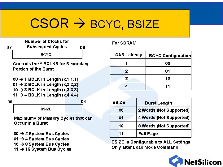
CSOR BCYC, BSIZE D 7 Number of Clocks for Subsequent Cycles D 6 For SDRAM CAS Latency BCYC Configuration Controls the # BCLKS for Secondary Portion of the Burst 1 00 2 01 00 1 BCLK in Length (x, 1, 1, 1) 01 2 BCLK in Length (x, 2, 2, 2) 10 3 BCLK in Length (x, 3, 3, 3) 11 4 BCLK in Length (x, 4, 4, 4) 3 10 4 11 D 4 D 5 BSIZE Burst Length 00 2 Words (Not Supported) Maximum# of Memory Cycles that can Occur in a Burst 01 4 Words (Not Supported) 10 8 Words (Not Supported) 00 2 System Bus Cycles 01 4 System Bus Cycles 10 8 System Bus Cycles 11 16 System Bus Cycles 11 Full Page BSIZE is Configurable to ALL Settings Only after Load Mode Command

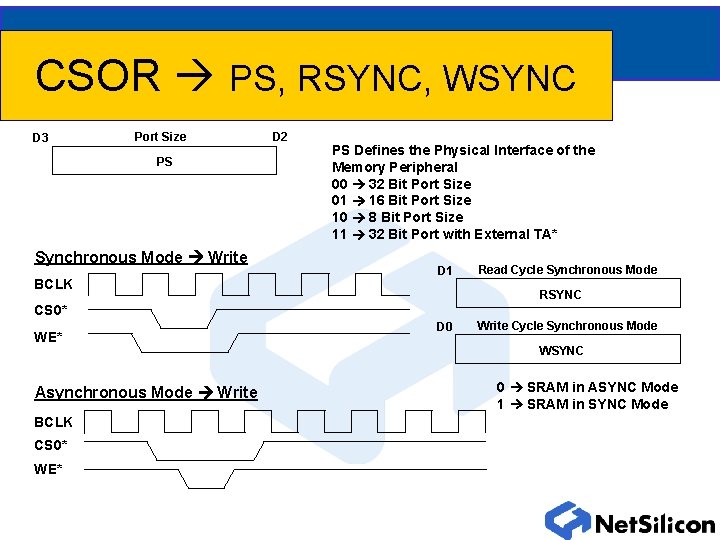
CSOR PS, RSYNC, WSYNC D 3 Port Size PS Synchronous Mode Write BCLK D 2 PS Defines the Physical Interface of the Memory Peripheral 00 32 Bit Port Size 01 16 Bit Port Size 10 8 Bit Port Size 11 32 Bit Port with External TA* D 1 Read Cycle Synchronous Mode RSYNC CS 0* WE* Asynchronous Mode Write BCLK CS 0* WE* D 0 Write Cycle Synchronous Mode WSYNC 0 SRAM in ASYNC Mode 1 SRAM in SYNC Mode

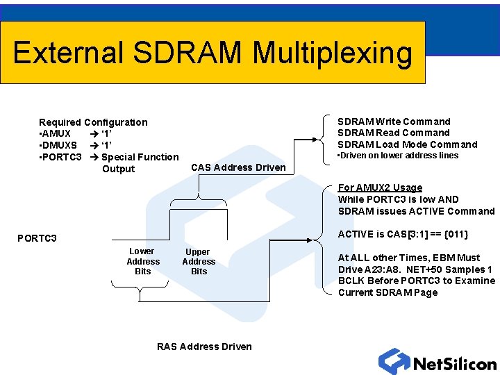
External SDRAM Multiplexing Required Configuration • AMUX ‘ 1’ • DMUXS ‘ 1’ • PORTC 3 Special Function Output SDRAM Write Command SDRAM Read Command SDRAM Load Mode Command • Driven on lower address lines CAS Address Driven For AMUX 2 Usage While PORTC 3 is low AND SDRAM issues ACTIVE Command ACTIVE is CAS[3: 1] == {011} PORTC 3 Lower Address Bits Upper Address Bits RAS Address Driven At ALL other Times, EBM Must Drive A 23: A 8. NET+50 Samples 1 BCLK Before PORTC 3 to Examine Current SDRAM Page

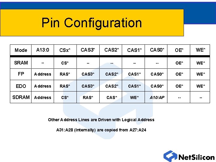
Pin Configuration Mode A 13: 0 CSx* CAS 3* CAS 2* CAS 1* CAS 0* OE* WE* SRAM -- CS* -- -- OE* WE* FP Address RAS* CAS 3* CAS 2* CAS 1* CAS 0* OE* WE* EDO Address RAS* CAS 3* CAS 2* CAS 1* CAS 0* OE* WE* CS* RAS* CAS* WE* A 10/AP -- -- SDRAM Address Other Address Lines are Driven with Logical Address A 31: A 28 (Internally) are copied from A 27: A 24

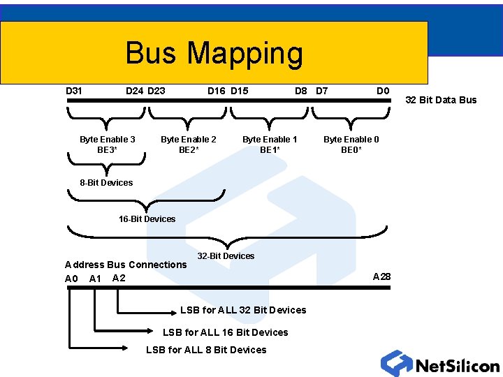
Bus Mapping D 31 D 24 D 23 Byte Enable 3 BE 3* D 16 D 15 Byte Enable 2 BE 2* D 8 D 7 Byte Enable 1 BE 1* D 0 Byte Enable 0 BE 0* 8 -Bit Devices 16 -Bit Devices Address Bus Connections A 0 A 1 A 2 32 -Bit Devices LSB for ALL 32 Bit Devices LSB for ALL 16 Bit Devices LSB for ALL 8 Bit Devices A 28 32 Bit Data Bus

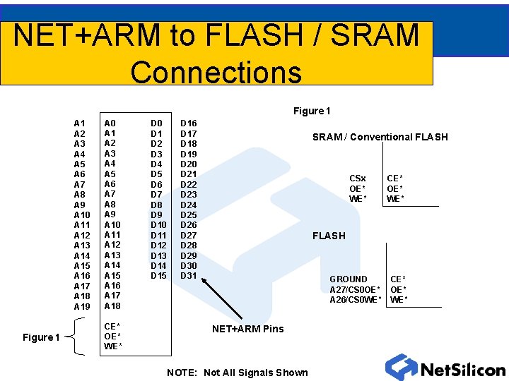
NET+ARM to FLASH / SRAM Connections Figure 1 A 2 A 3 A 4 A 5 A 6 A 7 A 8 A 9 A 10 A 11 A 12 A 13 A 14 A 15 A 16 A 17 A 18 A 19 Figure 1 A 0 A 1 A 2 A 3 A 4 A 5 A 6 A 7 A 8 A 9 A 10 A 11 A 12 A 13 A 14 A 15 A 16 A 17 A 18 CE* OE* WE* D 0 D 1 D 2 D 3 D 4 D 5 D 6 D 7 D 8 D 9 D 10 D 11 D 12 D 13 D 14 D 15 D 16 D 17 D 18 D 19 D 20 D 21 D 22 D 23 D 24 D 25 D 26 D 27 D 28 D 29 D 30 D 31 SRAM / Conventional FLASH CSx OE* WE* CE* OE* WE* FLASH GROUND A 27/CS 0 OE* A 26/CS 0 WE* NET+ARM Pins NOTE: Not All Signals Shown CE* OE* WE*

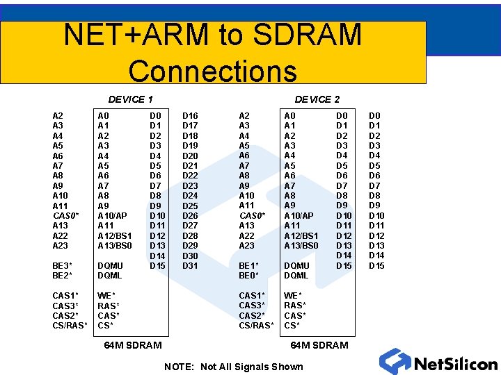
NET+ARM to SDRAM Connections DEVICE 2 DEVICE 1 A 2 A 3 A 4 A 5 A 6 A 7 A 8 A 9 A 10 A 11 CAS 0* A 13 A 22 A 23 A 0 A 1 A 2 A 3 A 4 A 5 A 6 A 7 A 8 A 9 A 10/AP A 11 A 12/BS 1 A 13/BS 0 BE 3* BE 2* DQMU DQML CAS 1* CAS 3* CAS 2* CS/RAS* WE* RAS* CS* D 0 D 1 D 2 D 3 D 4 D 5 D 6 D 7 D 8 D 9 D 10 D 11 D 12 D 13 D 14 D 15 64 M SDRAM D 16 D 17 D 18 D 19 D 20 D 21 D 22 D 23 D 24 D 25 D 26 D 27 D 28 D 29 D 30 D 31 A 2 A 3 A 4 A 5 A 6 A 7 A 8 A 9 A 10 A 11 CAS 0* A 13 A 22 A 23 A 0 A 1 A 2 A 3 A 4 A 5 A 6 A 7 A 8 A 9 A 10/AP A 11 A 12/BS 1 A 13/BS 0 BE 1* BE 0* DQMU DQML CAS 1* CAS 3* CAS 2* CS/RAS* WE* RAS* CS* D 0 D 1 D 2 D 3 D 4 D 5 D 6 D 7 D 8 D 9 D 10 D 11 D 12 D 13 D 14 D 15 64 M SDRAM NOTE: Not All Signals Shown D 0 D 1 D 2 D 3 D 4 D 5 D 6 D 7 D 8 D 9 D 10 D 11 D 12 D 13 D 14 D 15
![Static Memory Controller OE Output Enable SRAM Memory Devices WE Write Enable BE3 0 Static Memory Controller OE* Output Enable SRAM Memory Devices WE* Write Enable BE[3: 0]*](https://slidetodoc.com/presentation_image_h/02cac1483ef128f463ab4d294f49d904/image-24.jpg)
Static Memory Controller OE* Output Enable SRAM Memory Devices WE* Write Enable BE[3: 0]* Byte Enables Memory Controller FPGA RW* Read / Write Strobe ADDR[28: 0] Address Bus TA* Transfer Acknowledge A/D Converters TA* Transfer Acknowledge Myriad of SRAM Type Interface Devices Asynchronous SRAM cycles operate a minimum 1 wait state at ALL times

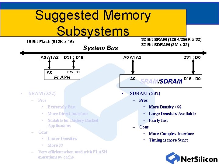
Suggested Memory Subsystems 32 Bit SRAM (128 K/256 K x 32) 32 Bit SDRAM (2 M x 32) 16 Bit Flash (512 K x 16) System Bus A 0 A 1 A 2 D 31 : D 16 A 0 D 15 : D 0 FLASH • SRAM (X 32) – – Pros D 31 : D 0 A 0 D 15 : D 0 SRAM/SDRAM (X 32) – Pros • Extremely Fast • More Density / $$ • More Direct Interface • Large Densities Available • Suitable for Battery Backed Applications • Fairly fast Cons • Lower Densities • More $$ – • A 0 A 1 A 2 Very efficient when used with FLASH executions w/ cache – Cons • More Complex Interface • Timing is more Strict

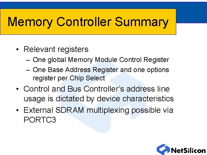
Memory Controller Summary • Relevant registers – One global Memory Module Control Register – One Base Address Register and one options register per Chip Select • Control and Bus Controller’s address line usage is dictated by device characteristics • External SDRAM multiplexing possible via PORTC 3