Photovoltaic Power Converter Students Thomas Carley Luke Ketcham


 ¨ VDSS n = 250 V")

 20 V – 66 V 13")
 20 V-66 V 14")


 n n n Every PV has a V-I and")
 Slight voltage perturbation n Observation of: n ¨ Change in")


 • Secondary Voltage of 10 VAC •")


 PWM n n n The magnitude of a triangle carrier")


 n Typically 0")


 mi = 0. 8 mf = 11 Vd = 200")
 mi = 0. 8 mf = 10 Vd = 200")
 Bipolar PWM Unipolar PWM 52")
 Bipolar PWM Unipolar PWM fout = 60 Hz (both cases) 53")


 Vout = 13. 6 V")


- Slides: 65
Photovoltaic Power Converter Students: Thomas Carley Luke Ketcham Brendan Zimmer Advisors: Dr. Woonki Na Dr. Brian Huggins Bradley University Department Of Electrical Engineering 5/1/12
Presentation Outline n Project Summary n Project Motivation n Overall System Block Diagram n Boost Converter n Inverter n Future Work 2
Project Summary n Photovoltaic Array n Supplies DC and AC Power n Boost Converter to step up PV voltage n Maximum Power Point Tracking n DC-AC converter for 120 Vrms 60 Hz n LC filter 3
Project Motivation Power Electronics n Alternative Energy Sources n Useful Applications n ¨ Household grid-tie inverter ¨ Electric drives 4
System Block Diagram 5
BP 350 J PV Panel n n n Pmax = 50 W Voltage at Pmax = 17. 5 V Current at Pmax = 2. 9 A Nominal Voltage = 12 V Isc = 3. 2 A Voc = 21. 8 V 6
DC Subsystem Requirements n The boost converter shall accept a voltage from the photovoltaic cells. ¨ The n input voltage shall be 48 Volts. average output shall be 200 Volts +/- 25 Volts. The voltage ripple shall be less than 20 Volts ¨ The open-loop boost converter shall operate above 65% efficiency. n The boost converter shall perform maximum power point tracking. ¨ The PWM of the boost converter shall be regulated based on current and voltage from the PV array. ¨ The efficiency of the MPPT system shall be above 80%. 7
Boost Converter Test Boost Converter 20 V to 66 V D =. 3 8
Boost Converter Design 9
Hardware 10
Key Components n MOSFET (IRFP 4768 Pb. F) ¨ VDSS n = 250 V Id = 93 A Ultrafast Diode (HFA 50 PA 60 C) ¨ VR = 600 V If = 25 A Trr = 50 ns Inductors (3 m. H) n Capacitors (6000 u. F) n 11
Gate Driver n IR 2110 12
Boost Converter Simulations Output Voltage (V) 20 V – 66 V 13
Boost Converter Simulations Boost Converter Current (A) 20 V-66 V 14
Boost Converter Testing 10 V to 16. 5 V 40% Duty Cycle Output Voltage Inductor Current 15
Eliminating Voltage Spikes Parasitic capacitance and inductance n Diode forward recovery time n Circuit Layout n Add Gate Resistor to increase turn-on and turn-off time n Add RC snubber n 16
Increasing Turn off Time Turn off time increased from 92 ns to 312 ns 17
Determining RC snubber values 18
Reducing Voltage Spikes 20 V to 66 V Without Gate Resistor And RC Snubber 70% duty With Gate Resistor And RC Snubber 19
Boost Converter Current Efficiency = 60. 7% Without RC snubber and Gate Resistor Efficiency = 58. 1% With RC snubber and Gate Resistor 20
Future Work For Boost Converter Optimize inductor value n Printed Circuit Board Layout n Optimize RC snubber values n Test with multiple solar panels n 21
Maximum Power Point Tracking (MPPT) n n n Every PV has a V-I and P-V curve for a given insolation and temperature The MPP is seen clearly from the P-V curve Anytime the system is not at the MPP, it is not at it’s most efficient point I V MPP P V 22
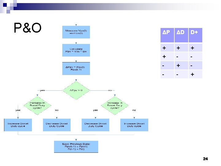
Perturb and Observe (P&O) Slight voltage perturbation n Observation of: n ¨ Change in PV power ¨ Change in boost converter duty cycle n Make an increase or decrease in boost converter duty cycle based on observation 23
MPPT Algorithm Comparison n Perturb and Observe ¨ Pros: n Very popular n Simple to implement ¨ Con: n Power loss from perturbation n Incremental Conductance ¨ Pro: n Tracks a rapidly changing MPP ¨ Cons: n Increased complexity n Increased susceptibility to noise 25
Implementing MPPT Spectrum Digital e. Zdsp F 2812 n Voltage Sensing n Current Sensing n Matlab Simulink Modeling with Code Composer Studio n 26
e. Zdsp F 2812 features n n n n Texas Instruments TMS 320 F 2812 chip 32 -bit DSP Core – 150 MIPS 18 K + 64 K RAM 128 K Flash 30 MHz clock 12 PWM outputs 16 ADC 12 bit inputs ¨ 60 ns conversion time 27
Voltage Sensing Vpv is 0 to 24 V n VADC 0 to 3. 3 V n 28
Current Sensing n Ipv: 0 to 50 A n Vout: 0 to 4 V 29
Simulink Model P&O n ADC measurement Voltage and current every 100μs ¨ Mean value with running window of 1 Hz ¨ 30
Simulink Model Soft Start 31
MPPT and Soft Start Results n Soft start duty cycle control ¨ 0% to 30% ¨ 5% increase every 5 seconds ¨ Transition to MPPT after 40 seconds n MPPT duty cycle control ¨ ADC measurements n Voltage and current every 100μs n Mean value with running window of 1 Hz ¨ 1% increase/decrease every 1 second 32
Power Supplies 120 Vrms 60 Hz input from wall n 15 V, and 3. 3 V output n Consists of Transformer, Diode Rectifier, 470 u. F capacitor, and voltage regulators n Needed for Gate Drivers, Op Amps, Sensing ICs, and other logic devices n 33
Power Supply Transformer (3 FL 20 -125) • Secondary Voltage of 10 VAC • Secondary Current of 0. 25 A RMS 34
Power Supply 35
AC Subsystem Overview 36
AC Subsystem Goals DC power to AC power n AC power quality n 37
AC Subsystem Requirements n The AC side of the system shall invert the output of the boost converter. ¨ The output of the inverter shall be AC voltage. ¨ The output shall be 60 Hz +/- 0. 1 Hz. n The inverter output shall be filtered by a LC filter. ¨ The filter shall remove high switching frequency harmonics. ¨ Total harmonic distortion of the output shall be less than 15%. 38
Topology - Inverter Single-phase bridge inverter 39
Switching Logic n Desire to control ¨ Output frequency ¨ Output magnitude Sinusoidal PWM! 40
Theory of Sinusoidal (Bipolar) PWM n n n The magnitude of a triangle carrier signal is compared to a sinusoidal reference If Vreference > Vcarrier PWM = high If Vreference < Vcarrier PWM = low A complementary signal drives opposite leg of H-bridge 41
Unipolar Sinusoidal PWM Two sinusoids compared to a triangle reference n Each comparison drives one H-bridge leg respectively n 42
Unipolar PWM in Action n n Two comparisons Each leg of H-bridge driven independently 3 -level output Less harmonic distortion than bipolar PWM 43
Design Equations n Modulation index, mi n Fundamental Output Magnitude n Frequency Modulation ratio, mf n Output Frequency 44
Implications n mi can be used to control output magnitude (voltage) n Typically 0 < mi ≤ 1 Overmodulation if mi > 1 (non -linear operation) ¨ Useful for obtaining large output power, but harmonic distortion will be large n 45
Implications n Output Frequency n Can select mf to remove even harmonics from output spectrum ¨ For Bipolar PWM, mf = odd integer ¨ For Unipolar PWM, mf = even integer Example (Unipolar): fcarrier = 60 Hz ftriangle = 2520 Hz mf = 42 46
Output n Desire sinusoidal output ¨ Output isn’t very sinusoidal n Use a filter ¨ LC filter 47
LC Filter n n n Goal: Smooth inverter output to smooth AC Second order LC filter transfer function: G(s) = 1/(L*C*s^2+1) fcarrier < cutoff frequency < fcarrier ∙ mf 48
Simulation n PSIM, Circuit Simulation Software ¨ Proof of concept simulations Bipolar PWM vs. Unipolar PWM n Effectiveness of LC filter with both schemes n 49
PSIM Schematic (Bipolar PWM) mi = 0. 8 mf = 11 Vd = 200 V 50
PSIM Schematic (Unipolar PWM) mi = 0. 8 mf = 10 Vd = 200 V 51
Simulation Result – Vout (unfiltered) Bipolar PWM Unipolar PWM 52
Simulation Results (filtered) Bipolar PWM Unipolar PWM fout = 60 Hz (both cases) 53
Bipolar PWM – Frequency Domain Unfiltered Output Filtered Output mi = 0. 8 mf = 81 54
Unipolar PWM – Frequency Domain Unfiltered Output Filtered Output mi = 0. 8 mf = 80 55
Implementation Major Hardware Components IGBT n Gate Drive n LC Filter n Spectrum Digital e. Zdsp F 2812 n ¨ Texas Instruments TMS 320 F 2812 ¨ Simulink, Code Composer Studio 56
IGBT n International Rectifier IRG 4 PC 30 UDPb. F ¨ VCEmax = 600 V ¨ fswitching max = 40 k. Hz ¨ ICmax = 12 A ¨ Cost = $2 -3 each 57
Gate Drive n International Rectifier IR 2110 ¨ Drives Two IGBTs/MOSFETs ¨ Cost $3 each 58
LC Filter L = 1 m. H C = 100 μF Cost of components = $6 fcutoff ≈ 500 Hz 59
Sinusoidal PWM – Simulink 60
Experimental Results Bipolar PWM Vd = 10 V (DC) Vout = 13. 6 V (AC) mi=0. 8 mf = 83 61
Future Work Closed-loop MPPT control with PV input n Inverter voltage and current controller n Tying the inverter to the grid n ¨ Phase Locked Loop (PLL) 62
Special thanks to: Dr. In Soo Ahn Mr. Steve Gutschlag 63
References n n n PV Module Simulink Models. ” ECEN 2060. University of Colorado Boulder. Rozenblat, Lazar. "A Grid Tie Inverter for Solar Systems. " Grid Tie Inverter Schematic and Principles of Operation. 6 Oct. 2011. <http: //solar. smps. us/grid-tie-inverter-schematic. html>. Tafticht, T. , K. Agbossou, M. Doumbia, and A. Cheriti. "An Improved Maximum Power Point Tracking Method for Photovoltaic Systems. " Renewable Energy 33. 7 (2008): 1508 -516. Tian, Yi. ANALYSIS, SIMULATION AND DSP BASED IMPLEMENTATION OF ASYMMETRIC THREE-LEVEL SINGLE-PHASE INVERTER IN SOLAR POWER SYSTEM. Thesis. Florida State University, 2007. Zhou, Lining. EVALUATION AND DSP BASED IMPLEMENTATION OF PWM APPROACHES FOR SINGLE-PHASE DC-AC CONVERTERS. Thesis. Florida State University, 2005. 64
Questions? 65