RF to DC Converter for Wireless Power Transfer
![Literature Review Fig 1. Efficiency of Full-Wave Rectifiers vs Input Power [1] 5 Literature Review Fig 1. Efficiency of Full-Wave Rectifiers vs Input Power [1] 5](https://slidetodoc.com/presentation_image_h/c28f66535d9353be67d0b136cb056efc/image-5.jpg)

![References [1] A. Boaventura, A. Collado, N. B. Carvalho, and A Georgiadis, "Optimum Behavior" References [1] A. Boaventura, A. Collado, N. B. Carvalho, and A Georgiadis, "Optimum Behavior"](https://slidetodoc.com/presentation_image_h/c28f66535d9353be67d0b136cb056efc/image-32.jpg)
- Slides: 34

RF to DC Converter for Wireless Power Transfer Systems Brandon White Advisor: Dr. Prasad Shastry

Agenda • Project Application • Project Overview • Literature Review • Block Diagram • Project Design • Simulation Results • Test Results • Conclusions 2

Project Application �Near-field wireless power transfer systems currently in use �Industry working towards far-field wireless power transfer systems 3

Project Overview • Convert radio frequency (RF) signal to direct current (DC) power • Functions in the FCC regulated ISM band that includes 5. 8 GHz • Output will be DC with minimal ripple • Maximize efficiency • Minimize size 4
![Literature Review Fig 1 Efficiency of FullWave Rectifiers vs Input Power 1 5 Literature Review Fig 1. Efficiency of Full-Wave Rectifiers vs Input Power [1] 5](https://slidetodoc.com/presentation_image_h/c28f66535d9353be67d0b136cb056efc/image-5.jpg)
Literature Review Fig 1. Efficiency of Full-Wave Rectifiers vs Input Power [1] 5

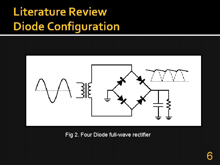
Literature Review Diode Configuration Fig 2. Four Diode full-wave rectifier 6

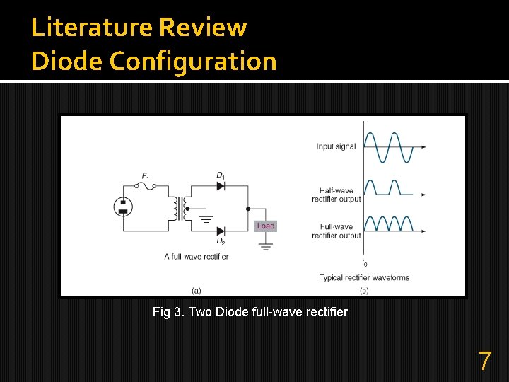
Literature Review Diode Configuration Fig 3. Two Diode full-wave rectifier 7

Literature Review �Not new concept �High gain antennas �Efficiency expectations 8

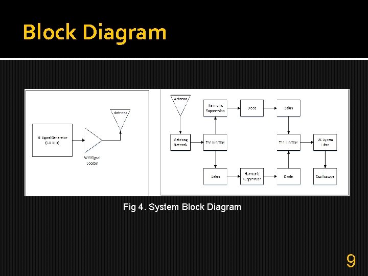
Block Diagram Fig 4. System Block Diagram 9

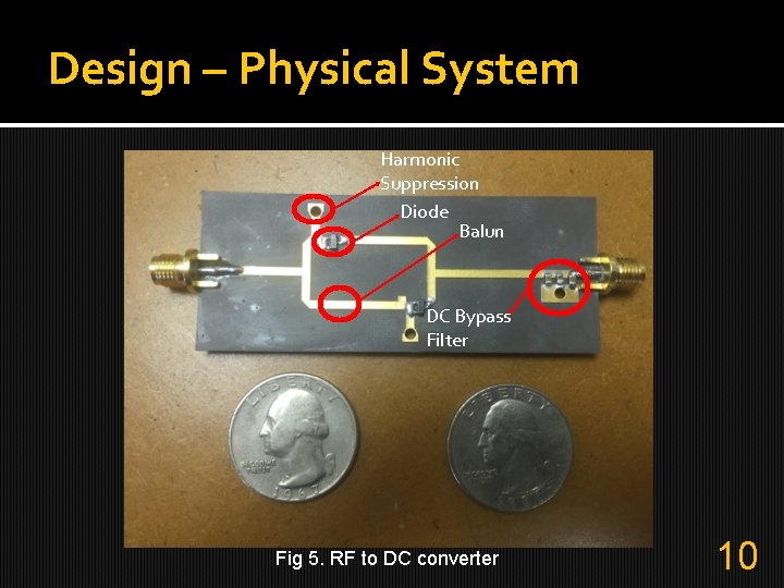
Design – Physical System Harmonic Suppression Diode Balun DC Bypass Filter Fig 5. RF to DC converter 10

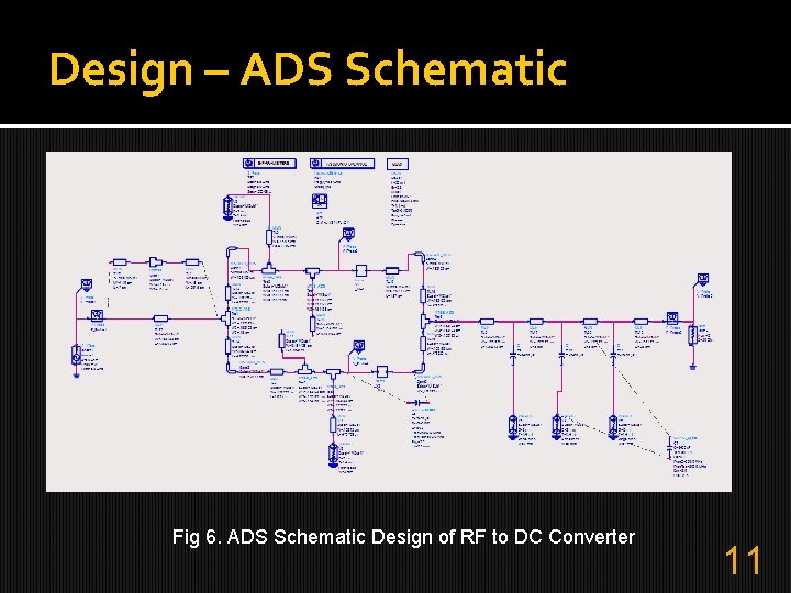
Design – ADS Schematic Fig 6. ADS Schematic Design of RF to DC Converter 11

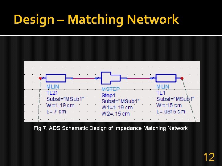
Design – Matching Network Fig 7. ADS Schematic Design of Impedance Matching Network 12

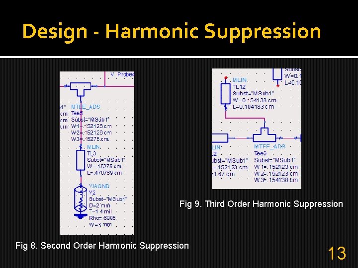
Design - Harmonic Suppression Fig 9. Third Order Harmonic Suppression Fig 8. Second Order Harmonic Suppression 13

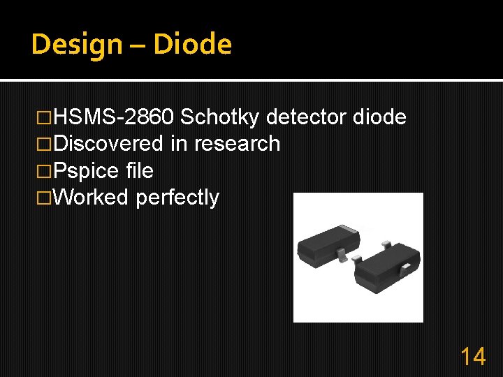
Design – Diode �HSMS-2860 Schotky detector �Discovered in research �Pspice file �Worked perfectly diode 14

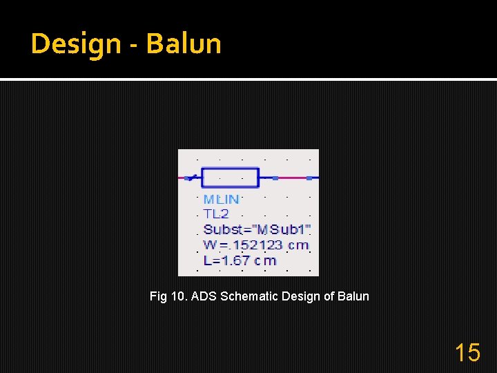
Design - Balun Fig 10. ADS Schematic Design of Balun 15

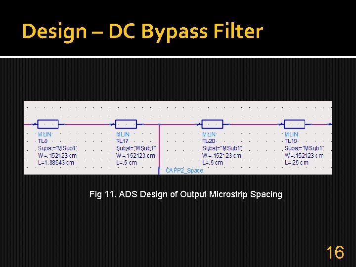
Design – DC Bypass Filter Fig 11. ADS Design of Output Microstrip Spacing 16

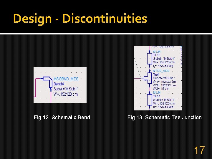
Design - Discontinuities Fig 12. Schematic Bend Fig 13. Schematic Tee Junction 17

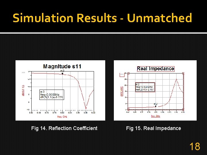
Simulation Results - Unmatched Fig 14. Reflection Coefficient Fig 15. Real Impedance 18

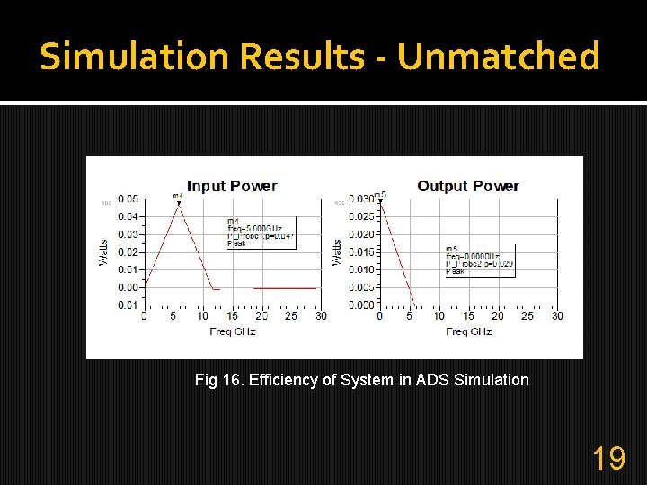
Simulation Results - Unmatched Fig 16. Efficiency of System in ADS Simulation 19

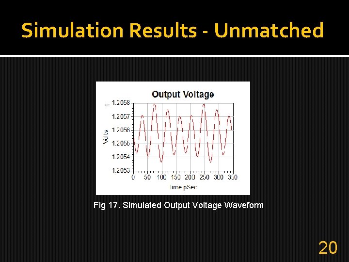
Simulation Results - Unmatched Fig 17. Simulated Output Voltage Waveform 20

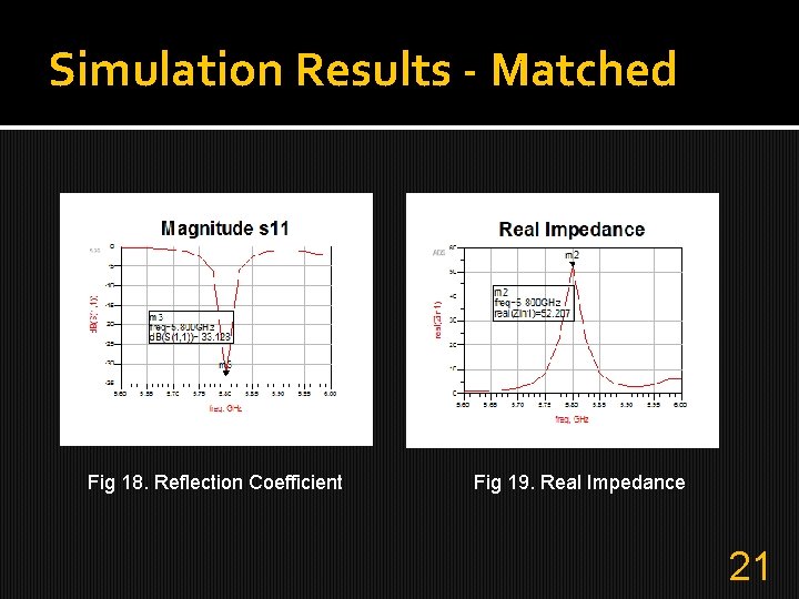
Simulation Results - Matched Fig 18. Reflection Coefficient Fig 19. Real Impedance 21

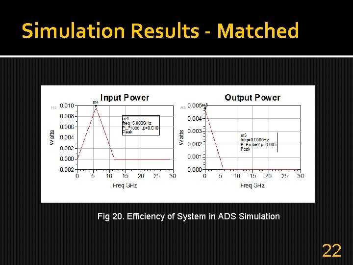
Simulation Results - Matched Fig 20. Efficiency of System in ADS Simulation 22

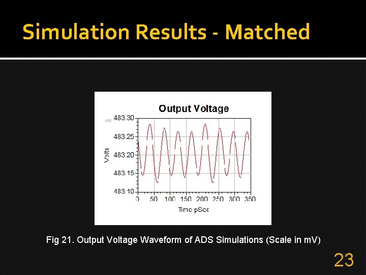
Simulation Results - Matched Fig 21. Output Voltage Waveform of ADS Simulations (Scale in m. V) 23

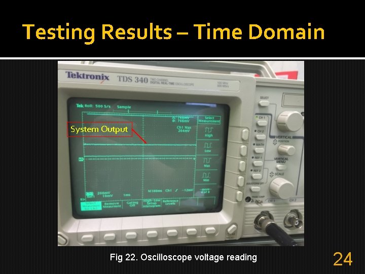
Testing Results – Time Domain System Output Fig 22. Oscilloscope voltage reading 24

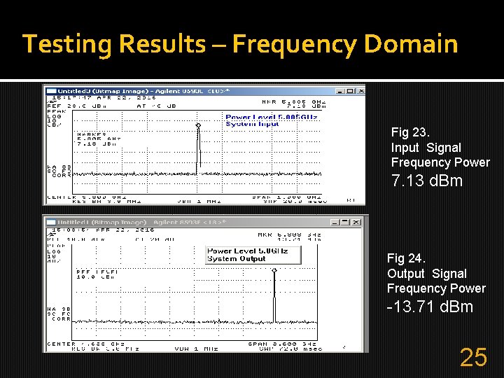
Testing Results – Frequency Domain Fig 23. Input Signal Frequency Power 7. 13 d. Bm Fig 24. Output Signal Frequency Power -13. 71 d. Bm 25

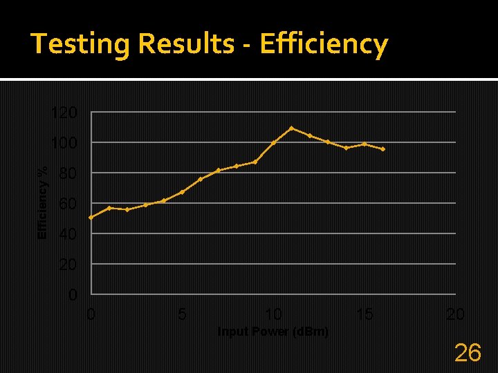
Testing Results - Efficiency 120 Efficiency % 100 80 60 40 20 0 0 5 10 15 20 Input Power (d. Bm) 26

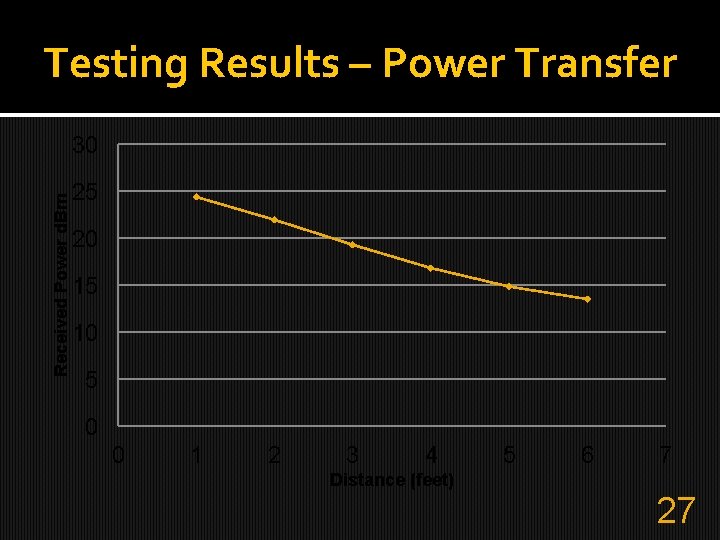
Testing Results – Power Transfer Received Power d. Bm 30 25 20 15 10 5 0 0 1 2 3 4 5 6 7 Distance (feet) 27

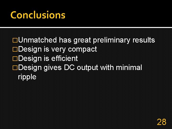
Conclusions �Unmatched has great preliminary results �Design is very compact �Design is efficient �Design gives DC output with minimal ripple 28

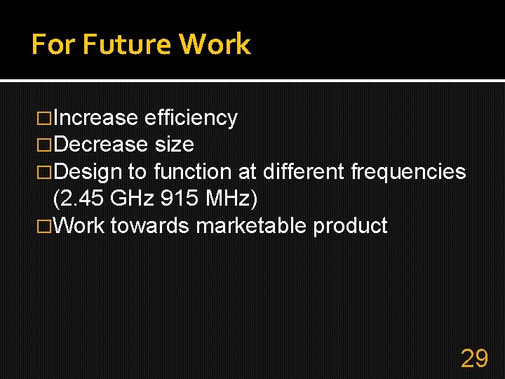
For Future Work �Increase efficiency �Decrease size �Design to function at different frequencies (2. 45 GHz 915 MHz) �Work towards marketable product 29

Special Thanks �Chris Mattus �Nick Schmidt �Bob Modica 30

Questions? 31
![References 1 A Boaventura A Collado N B Carvalho and A Georgiadis Optimum Behavior References [1] A. Boaventura, A. Collado, N. B. Carvalho, and A Georgiadis, "Optimum Behavior"](https://slidetodoc.com/presentation_image_h/c28f66535d9353be67d0b136cb056efc/image-32.jpg)
References [1] A. Boaventura, A. Collado, N. B. Carvalho, and A Georgiadis, "Optimum Behavior" in IEEE Microwave Mag. , vol. 14, no. 4, pp. 26 -35, 2013. � [2] Z. Popovic, "Cut the Cord" in IEEE Microwave Mag. , vol. 14, no. 4, pp. 55 -62, 2013 � [3] J. Zbitou, M. Latach, and S. Toutain, "Hybrid Rectenna and Monolithic Integrated Zero-Bias Microwave Rectifier" in IEEE Transactions on Microwave Theory and Techniques, vol. 54, no. 1, pp. 147 -152, 2006 � 32

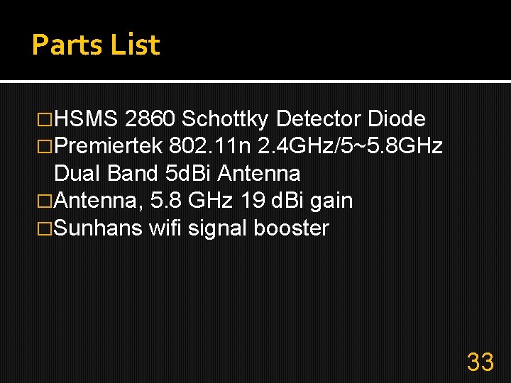
Parts List �HSMS 2860 Schottky Detector Diode �Premiertek 802. 11 n 2. 4 GHz/5~5. 8 GHz Dual Band 5 d. Bi Antenna �Antenna, 5. 8 GHz 19 d. Bi gain �Sunhans wifi signal booster 33

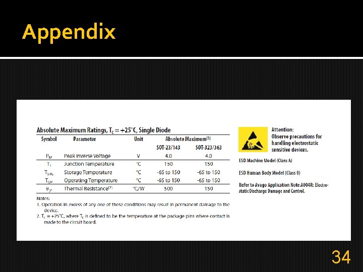
Appendix 34