Microprocessor and MicrocontrollerA 3419 Unit II 8086 MEMORY
- Slides: 58

Microprocessor and Microcontroller(A 3419) Unit – II 8086 MEMORY INTERFACING T. RAMAKRISHNAIAH Associate Professor Department of Electronics and Communication Engineering VARDHAMAN COLLEGE OF ENGINEERING Shamshabad, Hyderabad – 501218, India.

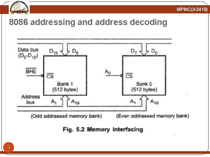
MPMC(A 3419) 8086 addressing and address decoding � Most of the memory ICs are byte oriented i. e. , each 2 memory location can store only one byte of data. � The 8086 is a 16 -bit microprocessor, it can transfer 16 -bit data. � So in addition to byte, word (16 -bit) has to be stored in the memory. � To implement this , the entire memory is divided into two memory banks: Bank 0 and Bank 1. � Bank 0 is selected only when A 0 is zero and Bank 1 is selected only when BHE’ is zero. � A 0 is zero for all even addresses, so Bank 0 is usually referred as even addressed memory bank. � BHE’ is used to access higher order memory bank, referred to as odd addressed memory bank.

MPMC(A 3419) 8086 addressing and address decoding 3

MPMC(A 3419) 8086 addressing and address decoding � Every microprocessor based system has a memory system. � Almost all systems contain two basic types of memory, 4 read only memory (ROM) and random access memory (RAM) or read/write memory. � ROM contains system software and permanent system data such as lookup tables, IVT. . etc. � RAM contains temporary data and application software. � ROMs/PROMs/EPROMs are mapped to cover the CPU’s reset address, since these are non-volatile. � When the 8086 is reset, the next instruction is fetched from the memory location FFFF 0 H. � So in the 8086 system the location FFFF 0 H must be in ROM location.

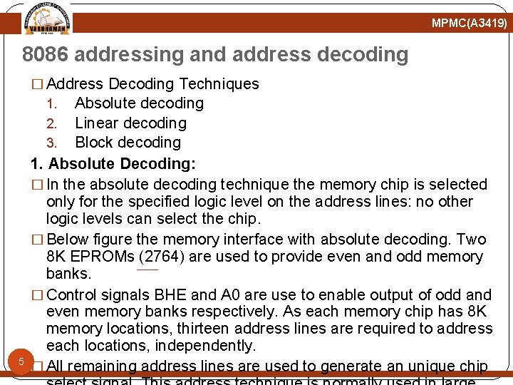
MPMC(A 3419) 8086 addressing and address decoding � Address Decoding Techniques 1. Absolute decoding 2. Linear decoding 3. Block decoding 5 1. Absolute Decoding: � In the absolute decoding technique the memory chip is selected only for the specified logic level on the address lines: no other logic levels can select the chip. � Below figure the memory interface with absolute decoding. Two 8 K EPROMs (2764) are used to provide even and odd memory banks. � Control signals BHE and A 0 are use to enable output of odd and even memory banks respectively. As each memory chip has 8 K memory locations, thirteen address lines are required to address each locations, independently. � All remaining address lines are used to generate an unique chip

MPMC(A 3419) Absolute Decoding: 6

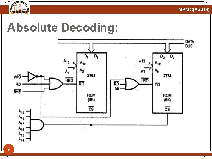
MPMC(A 3419) 8086 addressing and address decoding Linear Decoding: �In small system hardware for the decoding logic can be eliminated by using only required number of addressing lines (not all). �Other lines are simple ignored. This technique is referred as linear decoding or partial decoding. Control signals BHE and A 0 are used to enable odd and even memory banks, respectively. Figure shows the addressing of 16 K RAM (6264) with linear decoding. �The address line A 19 is used to select the RAM chips. When A 19 is low, chip is selected, otherwise it is disabled. �The status of A 14 to A 18 does not affect the chip 7 selection logic. This gives you multiple addresses

MPMC(A 3419) Linear Decoding: 8

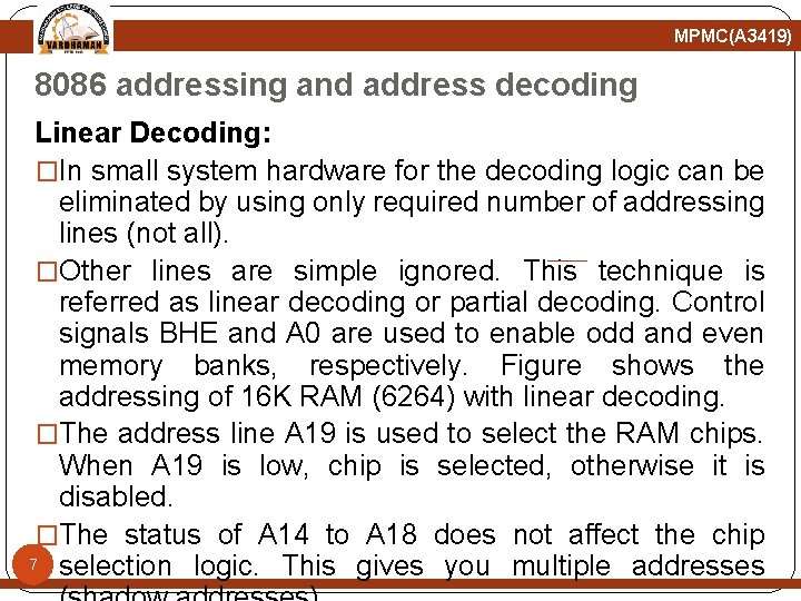
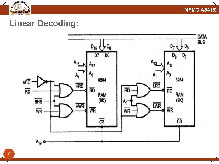
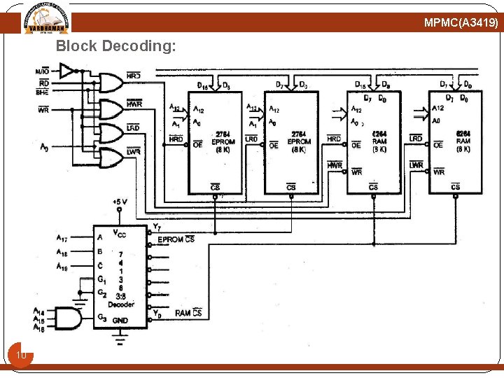
MPMC(A 3419) 8086 addressing and address decoding Block Decoding: �In a microcomputer system the memory array is often consists of several blocks of memory chips. �Each block of memory requires decoding circuit. To avoid separate decoding for each memory block special decoder IC is used to generate chip select signal for each block. �Figure shows the Block decoding technique using 74138, 3: 8 decoder 9

MPMC(A 3419) Block Decoding: 10

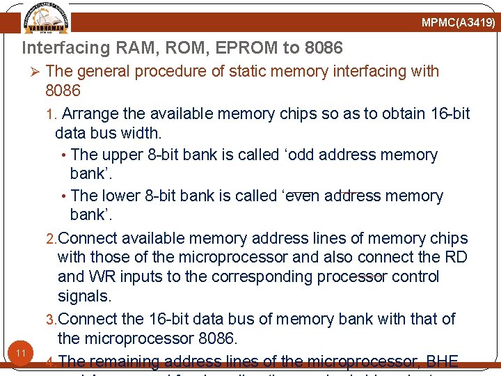
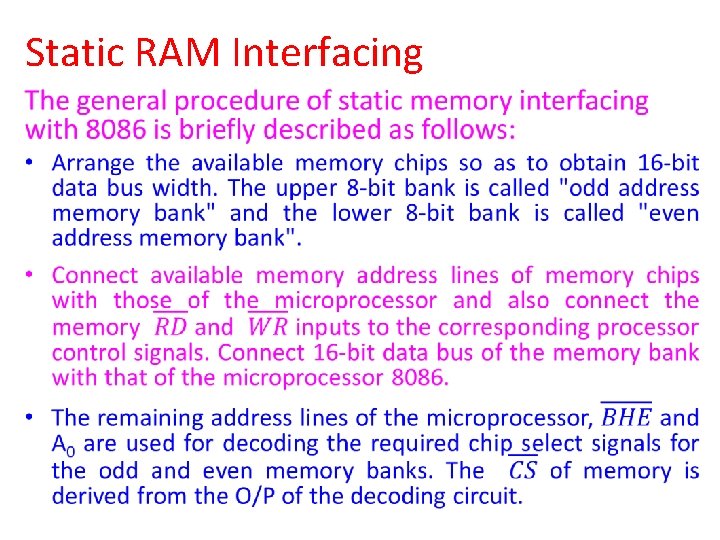
MPMC(A 3419) Interfacing RAM, ROM, EPROM to 8086 Ø The general procedure of static memory interfacing with 11 8086 1. Arrange the available memory chips so as to obtain 16 -bit data bus width. • The upper 8 -bit bank is called ‘odd address memory bank’. • The lower 8 -bit bank is called ‘even address memory bank’. 2. Connect available memory address lines of memory chips with those of the microprocessor and also connect the RD and WR inputs to the corresponding processor control signals. 3. Connect the 16 -bit data bus of memory bank with that of the microprocessor 8086. 4. The remaining address lines of the microprocessor, BHE

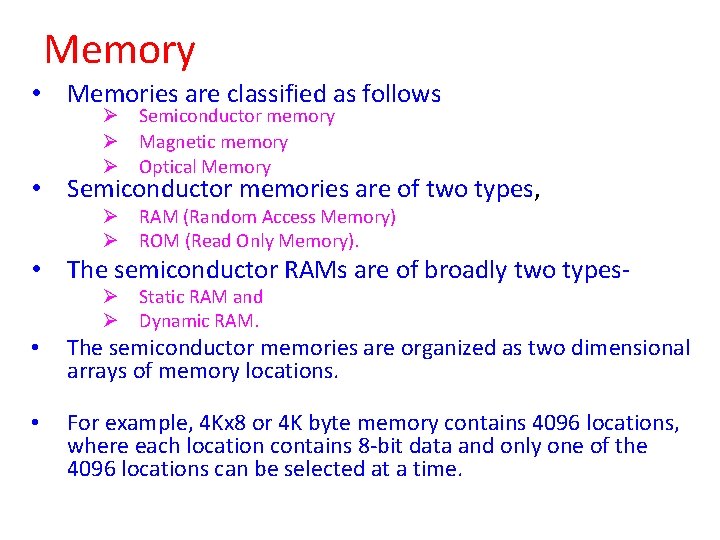
Memory • Memories are classified as follows Ø Semiconductor memory Ø Magnetic memory Ø Optical Memory • Semiconductor memories are of two types, Ø RAM (Random Access Memory) Ø ROM (Read Only Memory). • The semiconductor RAMs are of broadly two typesØ Static RAM and Ø Dynamic RAM. • The semiconductor memories are organized as two dimensional arrays of memory locations. • For example, 4 Kx 8 or 4 K byte memory contains 4096 locations, where each location contains 8 -bit data and only one of the 4096 locations can be selected at a time.

Static RAM Interfacing •

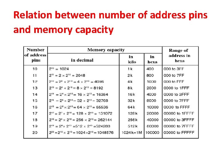
Relation between number of address pins and memory capacity

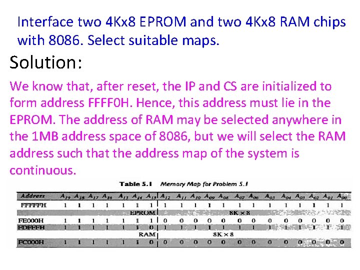
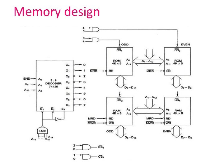
Interface two 4 Kx 8 EPROM and two 4 Kx 8 RAM chips with 8086. Select suitable maps. Solution: We know that, after reset, the IP and CS are initialized to form address FFFF 0 H. Hence, this address must lie in the EPROM. The address of RAM may be selected anywhere in the 1 MB address space of 8086, but we will select the RAM address such that the address map of the system is continuous.

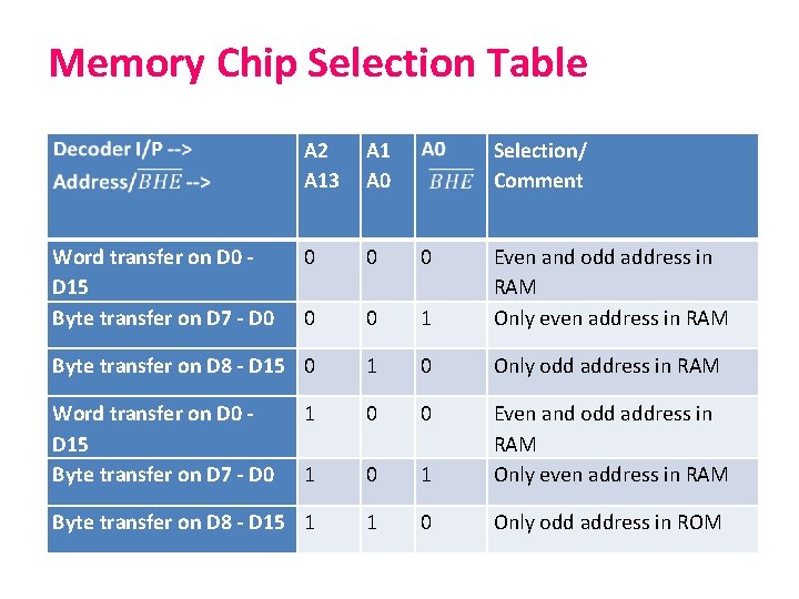
Memory Chip Selection Table A 2 A 13 A 1 A 0 0 0 1 Even and odd address in RAM Only even address in RAM Byte transfer on D 8 - D 15 0 1 0 Only odd address in RAM Word transfer on D 0 D 15 Byte transfer on D 7 - D 0 1 0 1 Even and odd address in RAM Only even address in RAM Byte transfer on D 8 - D 15 1 1 0 Only odd address in ROM Word transfer on D 0 D 15 Byte transfer on D 7 - D 0 Selection/ Comment

Memory design

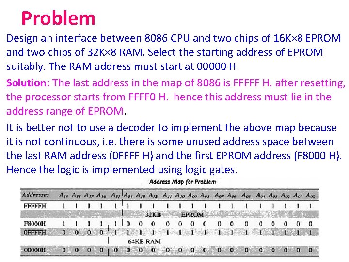
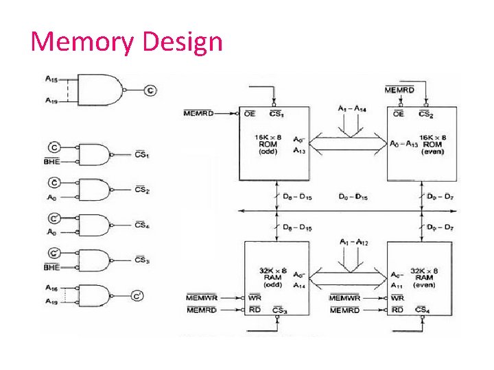
Problem Design an interface between 8086 CPU and two chips of 16 K× 8 EPROM and two chips of 32 K× 8 RAM. Select the starting address of EPROM suitably. The RAM address must start at 00000 H. Solution: The last address in the map of 8086 is FFFFF H. after resetting, the processor starts from FFFF 0 H. hence this address must lie in the address range of EPROM. It is better not to use a decoder to implement the above map because it is not continuous, i. e. there is some unused address space between the last RAM address (0 FFFF H) and the first EPROM address (F 8000 H). Hence the logic is implemented using logic gates.

Memory Design

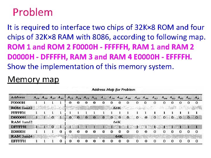
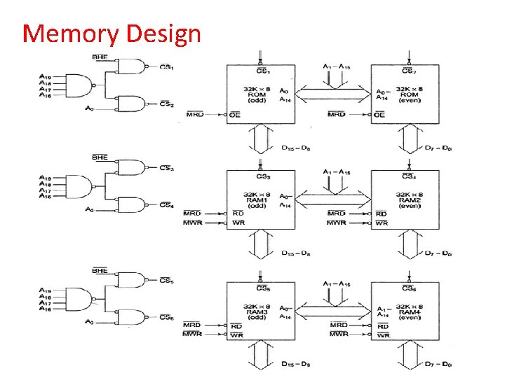
Problem It is required to interface two chips of 32 K× 8 ROM and four chips of 32 K× 8 RAM with 8086, according to following map. ROM 1 and ROM 2 F 0000 H - FFFFFH, RAM 1 and RAM 2 D 0000 H - DFFFFH, RAM 3 and RAM 4 E 0000 H - EFFFFH. Show the implementation of this memory system. Memory map

Memory Design

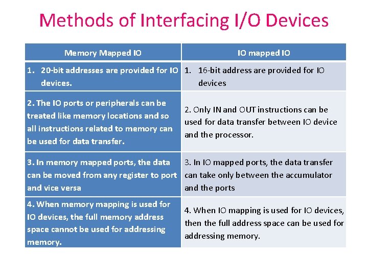
Methods of Interfacing I/O Devices Memory Mapped IO IO mapped IO 1. 20 -bit addresses are provided for IO 1. 16 -bit address are provided for IO devices 2. The IO ports or peripherals can be treated like memory locations and so all instructions related to memory can be used for data transfer. 2. Only IN and OUT instructions can be used for data transfer between IO device and the processor. 3. In memory mapped ports, the data 3. In IO mapped ports, the data transfer can be moved from any register to port can take only between the accumulator and vice versa and the ports 4. When memory mapping is used for IO devices, the full memory address space cannot be used for addressing memory. 4. When IO mapping is used for IO devices, then the full address space can be used for addressing memory.

Interfacing and Refreshing Dynamic RAMs MPMC(A 3419) �For small systems we need only a few kilobytes of RAM, we usually use static RAM devices because they are very easy to interface to. � For large systems we want several hundred kilobytes or mega bytes of memory, we use dynamic RAMs, often called DRAMs. �Static RAMs store each bit in an internal flip flop which requires four to six transistors. � In DRAMs a data bit is stored as a charge or no charge on a tiny capacitor. �All that is needed in addition to the capacitor is a single transistor switch to access the capacitor when a bit is written to it or read from it. 23

Interfacing and Refreshing Dynamic RAMs MPMC(A 3419) �The result of this is that DRAMs require much less power per bit, many more bits can be stored in a given chip. �This makes cost per bit of storage much less. �The disadvantage of DRAMs is that each stored bit must be refreshed because the charge stored on the tiny capacitors tends to change due to leakage. �The process of refreshing the data in the RAM is known as refresh cycle. �This activity is similar to reading the data from each cell of the memory and write back, independent of the 24 requirement of microprocessor, regularly.

Interfacing and Refreshing Dynamic RAMs MPMC(A 3419) �During this refresh period all other operations related to the memory subsystem are suspended. �Hence the refresh activity causes loss of time, resulting in reduce system performance. � However keeping in view the advantages of dynamic RAM, like low power consumption, high packaging density and low cost, most of the advanced computing system are designed using dynamic RAM, at the cost of operating speed. �A dedicated hardware chip called as dynamic RAM controller is the most important part of the interfacing circuit. 25

Interfacing and Refreshing Dynamic RAMs MPMC(A 3419) �Generally dynamic RAM is available in units of several Kilobits to even Megabits of memory (note that it is not in terms bytes or nibbles as in a static RAM). �This memory is arranged internally in a two dimensional matrix array so that it will have n rows and m columns. �The diagram shown in figure explains the refreshing logic and 8086 interfacing with dynamic RAM. �Each of the used chips 16 K * 1 -bit Dynamic RAM cell array. The system contains two 16 Kbytes Dynamic RAM units. �All the address and the data lines are assumed to be available from an 8086 microprocessor system. The 26 OE pin controls output data buffers of the memory chip.

Interfacing and Refreshing Dynamic RAMs MPMC(A 3419) 27

Interfacing and Refreshing Dynamic RAMs MPMC(A 3419) �The CE pins are active high chip select of memory chips. � The refresh cycle starts, if refresh output of the refresh timer goes high, OE’ and CE also tends to go to high. �The high CE enables the memory chip for refreshing, while high OE’ prevents the data from appearing on the data bus. �The 16 K× 1 - bit dynamic RAM has an internal array of 128× 128 cells, requiring 7 bits for row addresses. �The lower order seven lines A 0 -A 6 are multiplexed with refresh counter output A 10 -A 16. 28

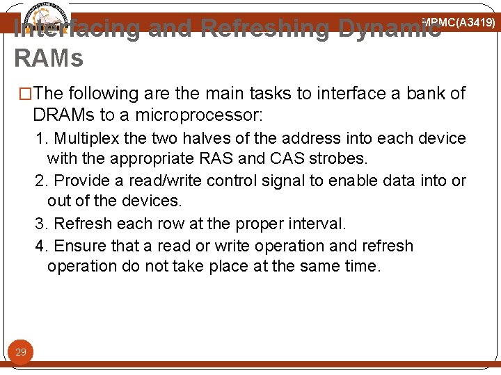
Interfacing and Refreshing Dynamic RAMs MPMC(A 3419) �The following are the main tasks to interface a bank of DRAMs to a microprocessor: 1. Multiplex the two halves of the address into each device with the appropriate RAS and CAS strobes. 2. Provide a read/write control signal to enable data into or out of the devices. 3. Refresh each row at the proper interval. 4. Ensure that a read or write operation and refresh operation do not take place at the same time. 29

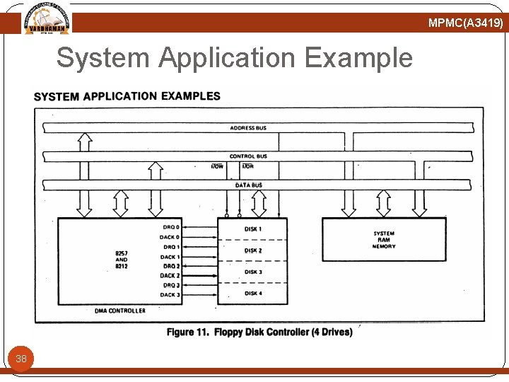
Direct Memory Access (DMA) Data Transfer MPMC(A 3419) �Direct Memory Access (DMA) is a feature of modern computer systems that allows certain hardware subsystems to read/write data to/from memory without microprocessor intervention, allowing the processor to do other work. �For facilitating DMA type of data transfer between several devices, a DMA controller may be used. 30

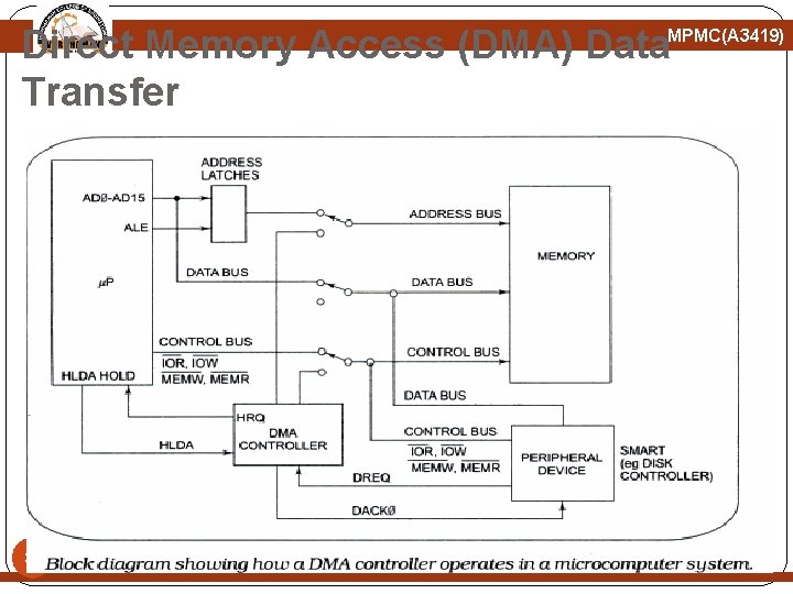
Direct Memory Access (DMA) Data Transfer MPMC(A 3419) 31

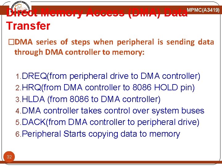
Direct Memory Access (DMA) Data Transfer MPMC(A 3419) �DMA series of steps when peripheral is sending data through DMA controller to memory: 1. DREQ(from peripheral drive to DMA controller) 2. HRQ(from DMA controller to 8086 HOLD pin) 3. HLDA (from 8086 to DMA controller) 4. DMA controller takes control over system buses 5. DACK(from DMA controller to peripheral drive) 6. Peripheral Starts copying data to memory 32

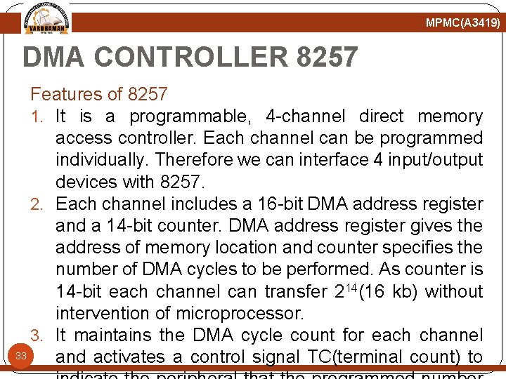
MPMC(A 3419) DMA CONTROLLER 8257 Features of 8257 1. It is a programmable, 4 -channel direct memory access controller. Each channel can be programmed individually. Therefore we can interface 4 input/output devices with 8257. 2. Each channel includes a 16 -bit DMA address register and a 14 -bit counter. DMA address register gives the address of memory location and counter specifies the number of DMA cycles to be performed. As counter is 14 -bit each channel can transfer 214(16 kb) without intervention of microprocessor. 3. It maintains the DMA cycle count for each channel 33 and activates a control signal TC(terminal count) to

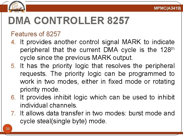
MPMC(A 3419) DMA CONTROLLER 8257 Features of 8257 4. It provides another control signal MARK to indicate peripheral that the current DMA cycle is the 128 th cycle since the previous MARK output. 5. It has the priority logic that resolves the peripheral requests. The priority logic can be programmed to work in two modes, either in fixed mode or rotating priority mode. 6. It provides inhibit logic which can be used to inhibit individual channels. 7. It allows data transfer in two modes: burst mode and cycle steal(single byte) mode. 34

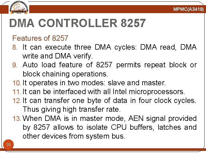
MPMC(A 3419) DMA CONTROLLER 8257 Features of 8257 8. It can execute three DMA cycles: DMA read, DMA write and DMA verify. 9. Auto load feature of 8257 permits repeat block or block chaining operations. 10. It operates in two modes: slave and master. 11. It can be interfaced with all Intel microprocessors. 12. It can transfer one byte of data in four clock cycles. Thus giving high transfer rate. 13. When DMA is in master mode, AEN signal provided by 8257 allows to isolate CPU buffers, latches and other devices from system bus. 35

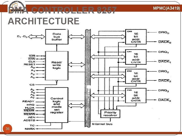
DMA CONTROLLER 8257 ARCHITECTURE 36 MPMC(A 3419)

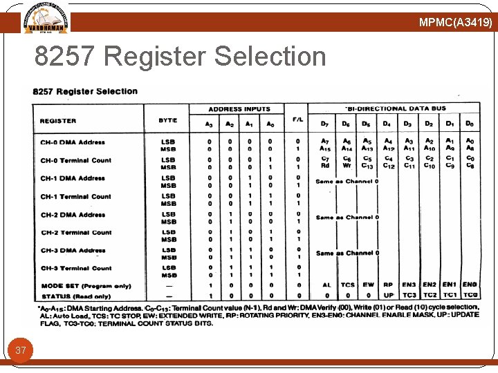
MPMC(A 3419) 8257 Register Selection 37

MPMC(A 3419) System Application Example 38

MPMC(A 3419) DMA CONTROLLER 8257 Data Bus Buffer: Ø It is a bi-directional, eight bit buffer which interfaces the 8257 to the system bus. Ø In the slave mode, it is used to transfer data between microprocessor and internal registers of 8257. Ø In master mode it is used to send higher byte address (A 8 -A 15) on the data bus. 39

MPMC(A 3419) DMA CONTROLLER 8257 Read/Write Logic: Ø When the CPU is programming or reading one of the internal registers of 8257(slave mode), the Read/Write logic accepts the I/O Read or I/O write signal, decodes the least significant four address bits(A 0 -A 3) and either writes the contents of data bus into the address register or places the contents of address register onto the data bus. Ø During DMA cycles(master mode) the Read/Write logic generates the I/O read and memory write(DMA write cycle) or I/O write and memory read(DMA read cycle signals which control the data transfer between 40 peripheral and memory devices.

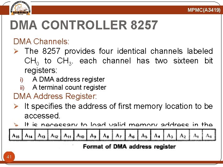
MPMC(A 3419) DMA CONTROLLER 8257 DMA Channels: Ø The 8257 provides four identical channels labeled CH 0 to CH 3. each channel has two sixteen bit registers: i) ii) A DMA address register A terminal count register DMA Address Register: Ø It specifies the address of first memory location to be accessed. Ø It is necessary to load valid memory address in the DMA address register before channel is enabled. 41

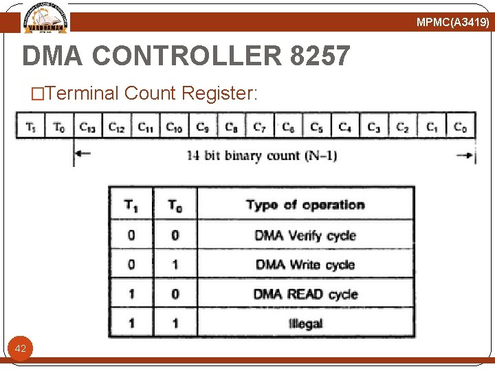
MPMC(A 3419) DMA CONTROLLER 8257 �Terminal Count Register: 42

MPMC(A 3419) DMA CONTROLLER 8257 Terminal Count Register: Ø The value loaded into lower order 14 bits(C 13 C 0) of the terminal count register specifies the number of DMA cycles minus one before the terminal count(TC) output is activated. Ø The most significant 2 bits of the terminal count register specifies the type of DMA operation to be performed. Ø It is necessary to load count for DMA cycles and operational code for valid DMA cycle in the 43 terminal count register before channel is enabled.

MPMC(A 3419) DMA CONTROLLER 8257 Control Logic: Ø It controls the sequence of operations during all DMA cycles(DMA write, DMA read, DMA verify) by generating the appropriate control signals and the 16 -bit address that specifies the memory location to be accessed. Ø It consists of two registers 1. Mode Set Register is programmed by CPU to configure 8257 2. Status Register is read by CPU to check which 44 channels have reached terminal count condition

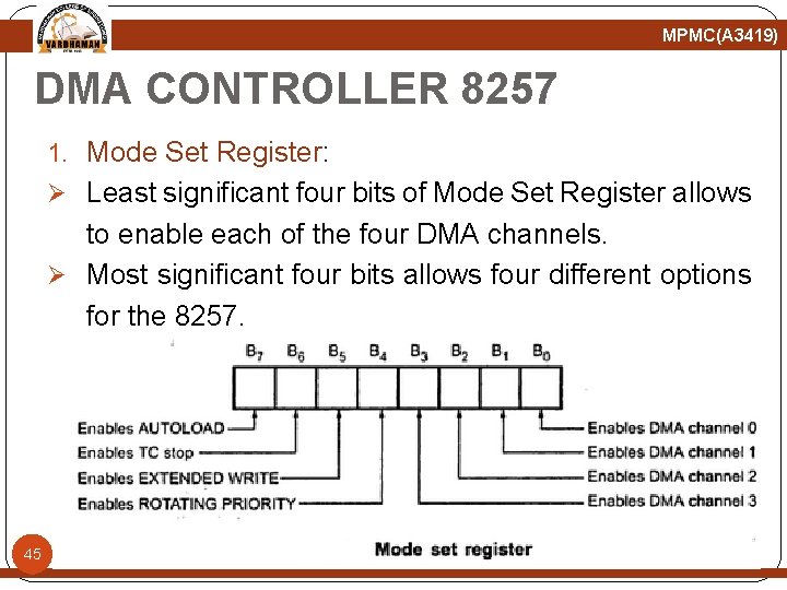
MPMC(A 3419) DMA CONTROLLER 8257 1. Mode Set Register: Ø Least significant four bits of Mode Set Register allows to enable each of the four DMA channels. Ø Most significant four bits allows four different options for the 8257. 45

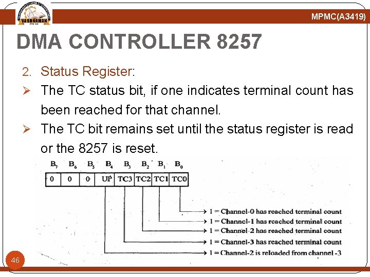
MPMC(A 3419) DMA CONTROLLER 8257 2. Status Register: Ø The TC status bit, if one indicates terminal count has been reached for that channel. Ø The TC bit remains set until the status register is read or the 8257 is reset. 46

MPMC(A 3419) DMA CONTROLLER 8257 Ø The update flag bit, if one indicates CPU that 8257 is executing update cycle. Ø In update cycle 8257 loads parameters in channel 3 to channel 2. Priority Resolver: Ø It resolves the peripherals requests. Ø It can be programmed to work in two modes 1. Fixed Mode 2. Rotating Priority Mode 47

MPMC(A 3419) DMA CONTROLLER 8257 Operating Modes of 8257 1. In rotating priority mode, the priority of the channels has a circular sequence. In this channel being serviced gets the lowest priority and the channel next to its gets the highest priority. 2. In the fixed priority channel 0 has the highest priority and channel 3 has lowest priority. 3. The extended write option provides alternative timing for the I/O and memory write signals which allows the devices to return an early READY and prevents the 48 unnecessary occurrence of wait states in 8257.

MPMC(A 3419) DMA CONTROLLER 8257 Operating Modes of 8257 4. If the TC STOP, bit is set, a channel is disabled after the terminal count output goes high thus automatically preventing further DMA operations on that channel. 5. Auto Load Mode when enabled, permits block chaining operations, without immediate software intervention between blocks. During the update cycle, it is necessary to prevent the CPU from inadvertently skipping a data block by overwriting a starting 49 address or terminal count in the channel 3 registers

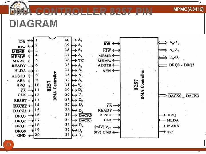
DMA CONTROLLER 8257 PIN DIAGRAM 50 MPMC(A 3419)

MPMC(A 3419) PIN Diagram Description DRQ 0 -DRQ 3: � These are the four individual channel DMA request inputs, used by the peripheral devices for requesting the DMA services. The DRQ 0 has the highest priority while DRQ 3 has the lowest one, if the fixed priority mode is selected. DACK 0 -DACK 3: � These are the active-low DMA acknowledge output lines which inform the requesting peripheral that the request has been honoured and the bus is relinquished by the CPU. These lines may act as strobe lines for the requesting devices. 51

MPMC(A 3419) PIN Diagram Description D 0 -D 7: � These are bidirectional, data lines used to interface the system bus with the internal data bus of 8257. These lines carry command words to 8257 and status word from 8257, in slave mode, i. e. under the control of CPU. � The data over these lines may be transferred in both the directions. When the 8257 is the bus master (master mode, i. e. not under CPU control), it uses D 0 -D 7 lines to send higher byte of the generated address to the latch. � This address is further latched using ADSTB signal. the address is transferred over D 0 -D 7 during the first clock cycle of the DMA cycle. During the rest of the period, data is available on the data bus. 52

MPMC(A 3419) PIN Diagram Description IOR: � This is an active-low bidirectional tristate input line that acts as an input in the slave mode. In slave mode, this input signal is used by the CPU to read internal registers of 8257. this line acts output in master mode. In master mode, this signal is used to read data from a peripheral during a memory write cycle. IOW: � This is an active low bidirection tristate line that acts as input in slave mode to load the contents of the data bus to the 8 -bit mode register or upper/lower byte of a 16 -bit DMA address register or terminal count register. In the master mode, it is a control output that loads the data to a peripheral during DMA memory read cycle (write to 53 peripheral).

MPMC(A 3419) PIN Diagram Description CLK: � This is a clock frequency input required to derive basic system timings for the internal operation of 8257. RESET: � This active-high asynchronous input disables all the DMA channels by clearing the mode register and tristates all the control lines. A 0 -A 3: � These are the four least significant address lines. In slave mode, they act as input which select one of the registers to be read or written. In the master mode, they are the four least significant memory address output lines generated by 8257. CS: � This is an active-low chip select line that enables the read/write operations from/to 8257, in slave mode. In the master mode, it is automatically disabled to prevent he chip from getting selected (by CPU) while performing the DMA operation. A 4 -A 7: 54� This is the higher nibble of the lower byte address generated by 8257 during the master mode of DMA operation.

MPMC(A 3419) PIN Diagram Description 55 READY: � This is an active-high asynchronous input used to stretch memory read and write cycles of 8257 by inserting wait states. This is used while interfacing slower peripherals. . HRQ: � The hold request output requests the access of the system bus. In the non cascaded 8257 systems, this is connected with HOLD pin of CPU. In the cascade mode, this pin of a slave is connected with a DRQ input line of the master 8257, while that of the master is connected with HOLD input of the CPU. HLDA: � The CPU drives this input to the DMA controller high, while granting the bus to the device. This pin is connected to the HLDA output of the CPU. This input, if high, indicates to the DMA controller that the bus has been granted to the requesting peripheral by the CPU. MEMR: � This active –low memory read output is used to read data from the addressed memory locations during DMA read cycles. MEMW: � This active-low three state output is used to write data to the addressed memory location during DMA write operation.

MPMC(A 3419) PIN Diagram Description ADST: � This output from 8257 strobes the higher byte of the memory address generated by the DMA controller into the latches. AEN: � This output is used to disable the system data bus and the control the bus driven by the CPU, this may be used to disable the system address and data bus by using the enable input of the bus drivers to inhibit the non-DMA devices from responding during DMA operations. If the 8257 is I/O mapped, this should be used to disable the other I/O devices, when the DMA controller addresses is on the address bus. Vcc: � This is a +5 v supply pin required for operation of the circuit. GND: � This is a return line for the supply (ground pin of the IC). 56

MPMC(A 3419) PIN Diagram Description TC: � Terminal count output indicates to the currently selected peripherals that the present DMA cycle is the last for the previously programmed data block. If the TC STOP bit in the mode set register is set, the selected channel will be disabled at the end of the DMA cycle. MARK: � The modulo 128 mark output indicates to the selected peripheral that the current DMA cycle is the 128 th cycle since the previous MARK output. The mark will be activated after each 128 cycles or integral multiples of it from the beginning if the data block (the first DMA cycle), if the total number of the required DMA cycles (n) is completely 57 divisible by 128.

MPMC(A 3419) Problem �Interface DMA controller 8257 with 8086 so that the channel 0 DMA address register has an I/O address 80 H and the mode set register has an address 88 H. Initialize the 8257 with normal priority , TC stop and non–extended write. Autoload is not required. The transfer is to take place using channel 0, write an ALP to move 2 KB of data from a peripheral device to memory address 2000: 5000 h, with the above initialization. �MODE SET REGISTER = ? �TERMINAL COUNT REGISTER= ? 58