Memory Hakim Weatherspoon CS 3410 Spring 2013 Computer

![SRAM Din[1] E. g. How do we design a 4 x 2 SRAM Module? SRAM Din[1] E. g. How do we design a 4 x 2 SRAM Module?](https://slidetodoc.com/presentation_image_h2/6e2894c6b22b6fe3d9645b079869da55/image-52.jpg)
![SRAM Din[1] E. g. How do we design a 4 x 2 SRAM Module? SRAM Din[1] E. g. How do we design a 4 x 2 SRAM Module?](https://slidetodoc.com/presentation_image_h2/6e2894c6b22b6fe3d9645b079869da55/image-53.jpg)
![SRAM E. g. How do we design a 4 x 2 SRAM Module? Din[1] SRAM E. g. How do we design a 4 x 2 SRAM Module? Din[1]](https://slidetodoc.com/presentation_image_h2/6e2894c6b22b6fe3d9645b079869da55/image-54.jpg)
![SRAM E. g. How do we design a 4 x 2 SRAM Module? Din[1] SRAM E. g. How do we design a 4 x 2 SRAM Module? Din[1]](https://slidetodoc.com/presentation_image_h2/6e2894c6b22b6fe3d9645b079869da55/image-58.jpg)
![SRAM Din[1] E. g. How do we design a 4 x 2 SRAM Module? SRAM Din[1] E. g. How do we design a 4 x 2 SRAM Module?](https://slidetodoc.com/presentation_image_h2/6e2894c6b22b6fe3d9645b079869da55/image-59.jpg)
- Slides: 71

Memory Hakim Weatherspoon CS 3410, Spring 2013 Computer Science Cornell University

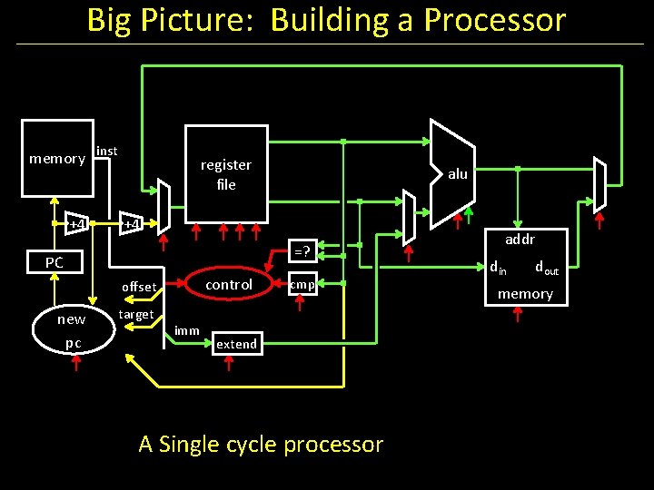
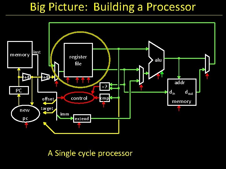
Big Picture: Building a Processor memory inst +4 register file +4 =? PC control offset new pc alu target imm cmp extend A Single cycle processor addr din dout memory

Goals for today Review • Finite State Machines Memory • • Register Files Tri-state devices SRAM (Static RAM—random access memory) DRAM (Dynamic RAM)

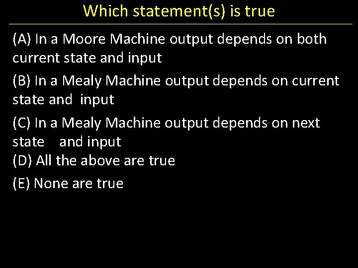
Which statement(s) is true (A) In a Moore Machine output depends on both current state and input (B) In a Mealy Machine output depends on current state and input (C) In a Mealy Machine output depends on next state and input (D) All the above are true (E) None are true

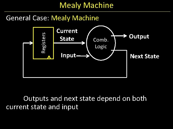
Mealy Machine Registers General Case: Mealy Machine Current State Input Comb. Logic Output Next State Outputs and next state depend on both current state and input

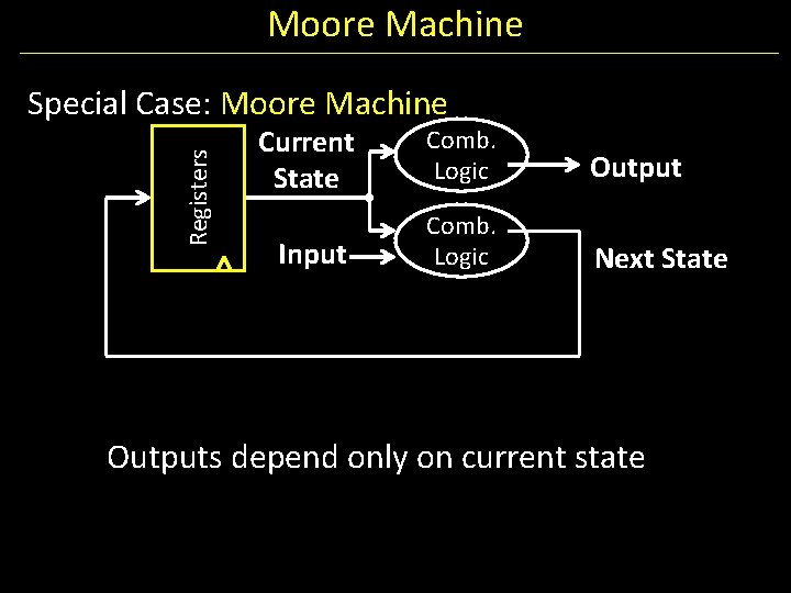
Moore Machine Registers Special Case: Moore Machine Current State Comb. Logic Output Input Comb. Logic Next State Outputs depend only on current state

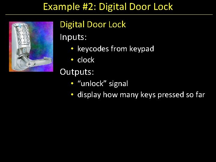
Example #2: Digital Door Lock Inputs: • keycodes from keypad • clock Outputs: • “unlock” signal • display how many keys pressed so far

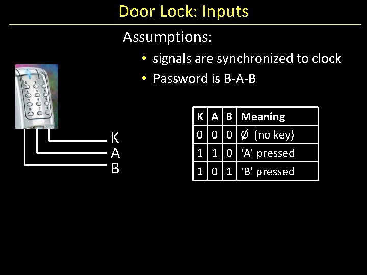
Door Lock: Inputs Assumptions: • signals are synchronized to clock • Password is B-A-B K A B K 0 1 1 A 0 1 0 B 0 0 1 Meaning Ø (no key) ‘A’ pressed ‘B’ pressed

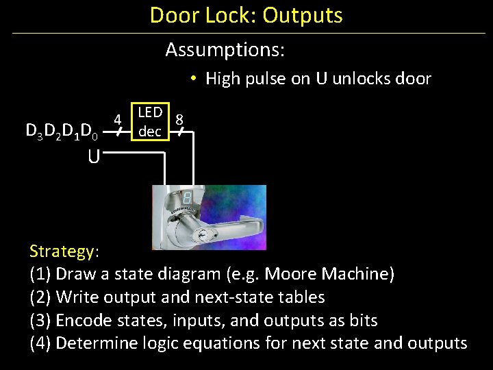
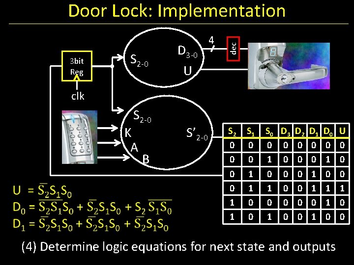
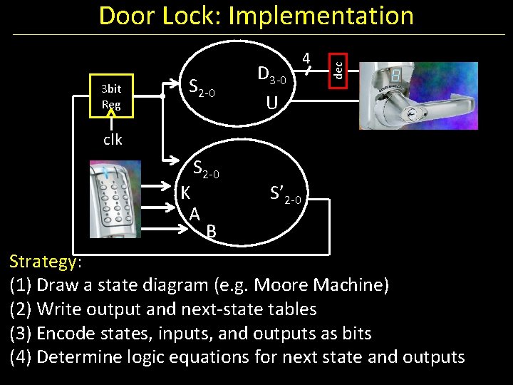
Door Lock: Outputs Assumptions: • High pulse on U unlocks door D 3 D 2 D 1 D 0 4 LED 8 dec U Strategy: (1) Draw a state diagram (e. g. Moore Machine) (2) Write output and next-state tables (3) Encode states, inputs, and outputs as bits (4) Determine logic equations for next state and outputs

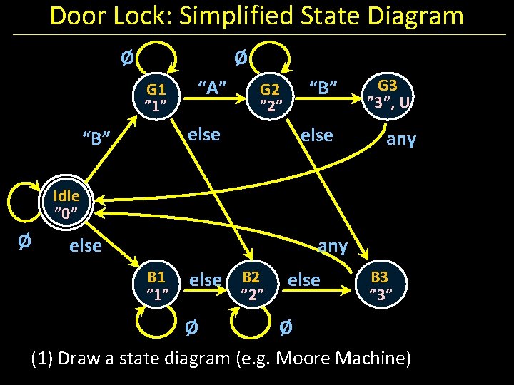
Door Lock: Simplified State Diagram Ø Ø G 1 ” 1” “A” “B” G 2 ” 2” else “B” else G 3 ” 3”, U any Idle ” 0” Ø else any B 1 ” 1” else B 2 ” 2” Ø else B 3 ” 3” Ø (1) Draw a state diagram (e. g. Moore Machine)

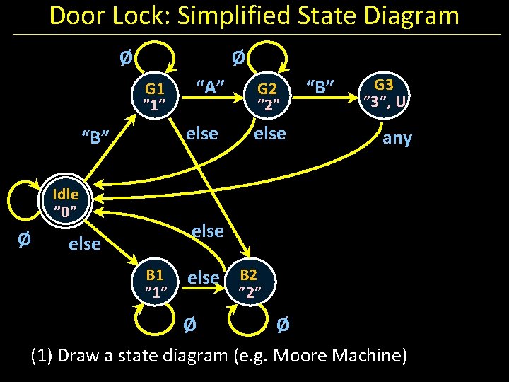
Door Lock: Simplified State Diagram Ø Ø G 1 ” 1” else “B” Idle ” 0” Ø “A” G 2 ” 2” else “B” G 3 ” 3”, U any else B 1 ” 1” else B 2 ” 2” Ø Ø (1) Draw a state diagram (e. g. Moore Machine)

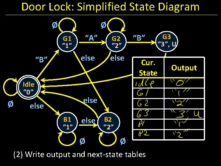
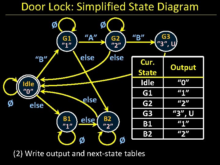
Door Lock: Simplified State Diagram Ø Ø G 1 ” 1” else “B” Idle ” 0” Ø “A” G 2 ” 2” else “B” Cur. any Output State else B 1 ” 1” else B 2 ” 2” Ø G 3 ” 3”, U Ø (2) Write output and next-state tables

Door Lock: Simplified State Diagram Ø Ø G 1 ” 1” else “B” Idle ” 0” Ø “A” G 2 ” 2” else B 1 ” 1” else B 2 ” 2” Ø Ø “B” G 3 ” 3”, U Cur. any Output State Idle “ 0” G 1 “ 1” G 2 “ 2” G 3 “ 3”, U B 1 “ 1” B 2 “ 2” (2) Write output and next-state tables

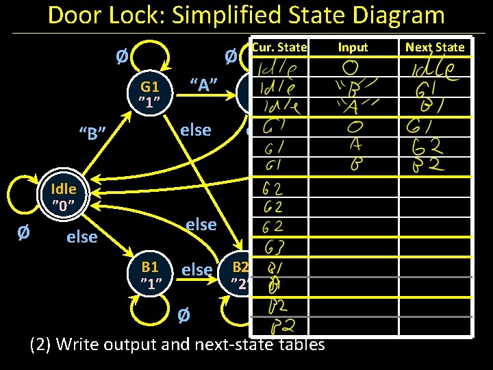
Door Lock: Simplified State Diagram Ø Ø G 1 ” 1” “A” else “B” Idle ” 0” Ø Cur. State G 2 ” 2” “B” else B 1 ” 1” else B 2 ” 2” Ø Ø (2) Write output and next-state tables Input Next State G 3 ” 3”, U any

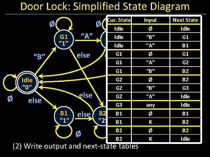
Door Lock: Simplified State Diagram Ø G 1 ” 1” else “B” Idle ” 0” Ø “A” else B 1 ” 1” else Cur. State Ø Idle G 2 Idle “B” ” 2”Idle else. G 1 G 1 G 2 G 2 G 3 B 2 B 1 ” 2” B 1 B 2 Ø (2) Write output and next-state tables Input Next State Ø Idle “B”G 3 G 1 ” 3”, U “A” B 1 Ø any G 1 “A” G 2 “B” B 2 Ø B 2 “B” G 3 “A” Idle any Idle Ø B 1 K B 2 Ø B 2 K Idle

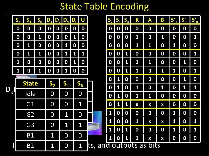
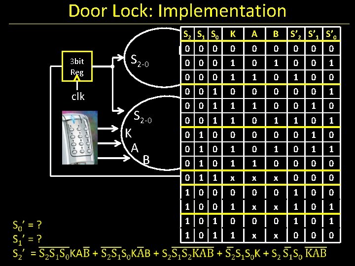
State Table Encoding SCur. SState S 0 D 3 2 1 0 Idle 0 0 G 1 0 0 G 2 1 0 0 0 G 3 1 1 0 1 B 1 0 0 0 1 B 2 0 1 0 DOutput 2 D 1 D 0 0 “ 0” 0 0 0 “ 1” 0 1 0 “ 2” 1 0 0“ 3”, 1 U 1 0 “ 1” 0 1 0 “ 2” 1 0 U 0 0 0 1 0 0 State S 2 S 1 8 S 0 4 Meaning K A B D 3 D 2 D 1 D 0 dec Idle 0 0 Ø (no 0 key) 0 U 0 0 1 G 1 1 1 0 ‘A’ pressed K 0 G 2 0 1 1 0 1 ‘B’ pressed A 1 B Cur. S 2 SState 1 S 0 0 Idle 0 0 0 G 1 0 1 0 G 2 1 0 0 G 3 1 1 1 B 1 0 0 1 B 2 0 1 K Input A B 0 Ø 0 0 1 “B” 0 1 1 “A” 1 0 0 Ø 0 0 1 “A” 1 0 1 “B” 0 1 0 Ø 0 0 1 “B” 0 1 1 “A” 1 0 x any x x 0 Ø 0 0 1 K x x G 3 0 1 B 1 1 0 0 (3) Encode states, and outputs as bits B 2 1 0 inputs, 1 Next S’ 2 S’State 1 S’ 0 0 Idle 0 0 0 G 1 0 1 1 B 1 0 0 0 G 1 0 G 2 1 0 1 B 2 0 1 0 B 2 1 0 0 G 3 1 1 0 Idle 0 0 1 B 1 0 0 1 B 2 0 1 0 Idle 0 0

3 bit Reg S 2 -0 D 3 -0 U 4 dec Door Lock: Implementation clk S 2 -0 K A B S’ 2 -0 S 2 0 0 1 1 S 1 0 0 1 1 0 0 S 0 D 3 0 0 1 0 D 2 0 0 0 D 1 0 0 1 1 0 1 D 0 0 1 1 0 (4) Determine logic equations for next state and outputs U 0 0 0 1 0 0

Door Lock: Implementation 3 bit Reg clk S 2 -0 K A B K 0 1 1 x 0 1 dec S 2 -0 S 2 S 1 S 0 4 D 03 -00 0 0 U 0 0 0 1 0 S’ 2 -0 1 0 0 1 1 1 0 0 1 0 1 A 0 0 1 0 0 0 1 x 0 x B 0 1 0 0 0 1 0 x 0 x S’ 2 S’ 1 S’ 0 0 0 1 1 0 0 1 0 1 0 1 0 0 1 1 0 0 0

3 bit Reg S 2 -0 D 3 -0 U 4 dec Door Lock: Implementation clk S 2 -0 K A S’ 2 -0 B Strategy: (1) Draw a state diagram (e. g. Moore Machine) (2) Write output and next-state tables (3) Encode states, inputs, and outputs as bits (4) Determine logic equations for next state and outputs

Administrivia Make sure to go to your Lab Section this week • • • Find project partners this week (for upcoming project 1 next week) Lab 2 due in class this week (it is not homework) Design Doc for Lab 1 due yesterday, Monday, Feb 4 th Completed Lab 1 due next week, Monday, Feb 11 th Work alone Homework 1 is due Wednesday • Work alone • Academic Integrity BUT, use your resources • Lab Section, Piazza. com, Office Hours, Homework Help Session, • Class notes, book, Sections, CSUGLab Second C Primer: Thursday, B 14 Hollister, 6 -8 pm

Administrivia Check online syllabus/schedule • http: //www. cs. cornell. edu/Courses/CS 3410/2013 sp/schedule. html Slides and Reading for lectures Office Hours Homework and Programming Assignments Prelims (in evenings): • Tuesday, February 26 th • Thursday, March 28 th • Thursday, April 25 th Schedule is subject to change

Collaboration, Late, Re-grading Policies “Black Board” Collaboration Policy • Can discuss approach together on a “black board” • Leave and write up solution independently • Do not copy solutions Late Policy • Each person has a total of four “slip days” • Max of two slip days for any individual assignment • Slip days deducted first for any late assignment, cannot selectively apply slip days • For projects, slip days are deducted from all partners • 25% deducted per day late after slip days are exhausted Regrade policy • Submit written request to lead TA, and lead TA will pick a different grader • Submit another written request, lead TA will regrade directly • Submit yet another written request for professor to regrade.

Lab 1: Thoughts thus far Great experience! But, read all instructions (multiple times)! Sign up for design doc meetings early • We were very lenient for Lab 1 • In future, CMS will lock the Friday after release • lose points for not signing up before lock, canceling last minute, and/or not showing up Design doc meeting • Not the same as office hours You are presenting your current design during design doc meeting • Bring printout of your design document • TA will grade and give feedback based on your presentation of your design

Goals for today Memory • • CPU: Register Files (i. e. Memory w/in the CPU) Scaling Memory: Tri-state devices Cache: SRAM (Static RAM—random access memory) Memory: DRAM (Dynamic RAM)

Goal: How do we store results from ALU computations? How do we use stored results in subsequent operations? Register File How does a Register File work? How do we design it?

Big Picture: Building a Processor memory inst +4 register file +4 =? PC control offset new pc alu target imm cmp extend A Single cycle processor addr din dout memory

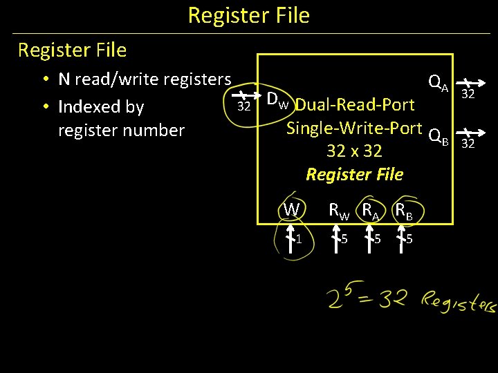
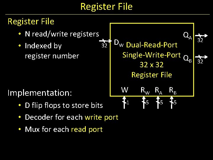
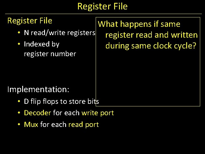
Register File • N read/write registers QA 32 DW Dual-Read-Port • Indexed by Single-Write-Port Q register number B 32 x 32 Register File W 1 RW RA RB 5 5 5 32 32

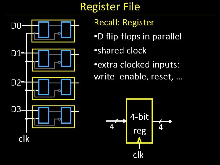
Register File D 0 D 1 D 2 Recall: Register • D flip-flops in parallel • shared clock • extra clocked inputs: write_enable, reset, … D 3 4 clk 4 -bit reg 4 clk

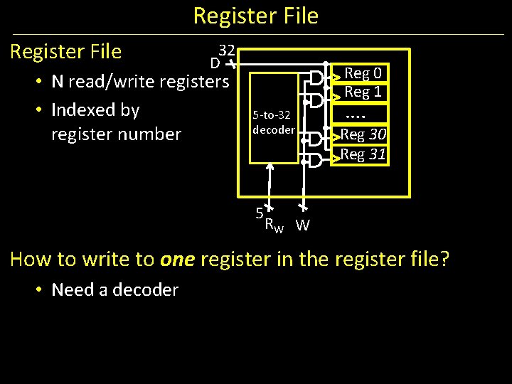
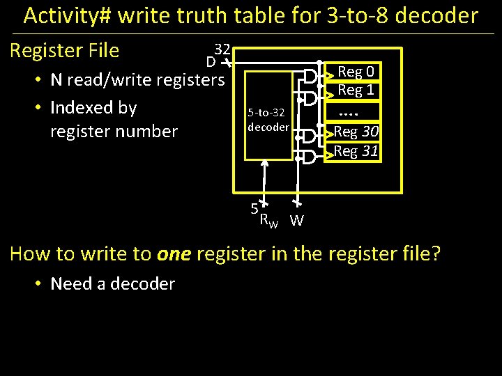
Register File 32 D • N read/write registers • Indexed by register number Reg 0 Reg 1 5 -to-32 decoder 5 …. Reg 30 Reg 31 RW W How to write to one register in the register file? • Need a decoder

Activity# write truth table for 3 -to-8 decoder Register File 32 D • N read/write registers • Indexed by register number Reg 0 Reg 1 5 -to-32 decoder 5 …. Reg 30 Reg 31 RW W How to write to one register in the register file? • Need a decoder

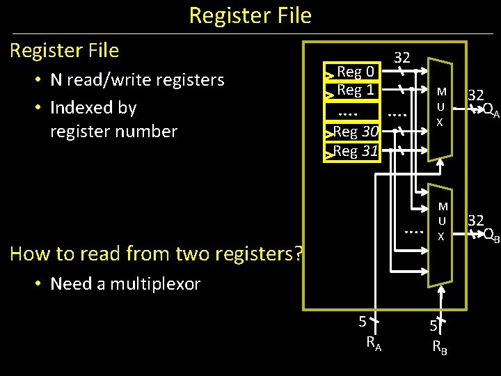
Register File • N read/write registers • Indexed by register number Reg 0 Reg 1 …. Reg 30 Reg 31 32 …. How to read from two registers? M U X • Need a multiplexor 5 RA 5 RB 32 QA 32 QB

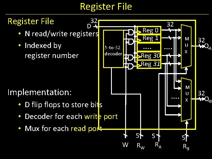
Register File 32 D • N read/write registers • Indexed by register number Reg 0 Reg 1 5 -to-32 decoder …. Reg 30 Reg 31 Implementation: • D flip flops to store bits • Decoder for each write port • Mux for each read port 32 …. 5 5 W RW RA M U X 5 RB 32 QA 32 QB

Register File • N read/write registers QA 32 DW Dual-Read-Port • Indexed by Single-Write-Port Q register number B 32 x 32 Register File Implementation: • D flip flops to store bits • Decoder for each write port • Mux for each read port W 1 RW RA RB 5 5 5 32 32

Register File What happens if same • N read/write registers register read and written • Indexed by during same clock cycle? register number Implementation: • D flip flops to store bits • Decoder for each write port • Mux for each read port

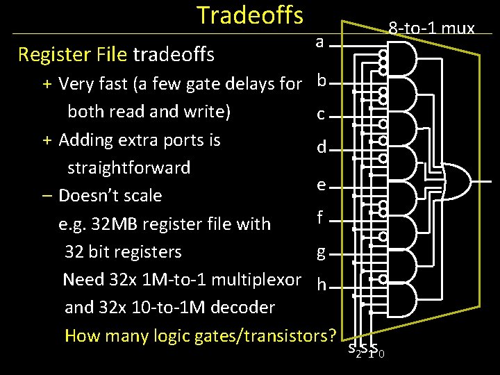
Tradeoffs Register File tradeoffs 8 -to-1 mux a + Very fast (a few gate delays for b both read and write) c + Adding extra ports is d straightforward e – Doesn’t scale f e. g. 32 MB register file with g 32 bit registers Need 32 x 1 M-to-1 multiplexor h and 32 x 10 -to-1 M decoder How many logic gates/transistors? s 2 s 1 s 0

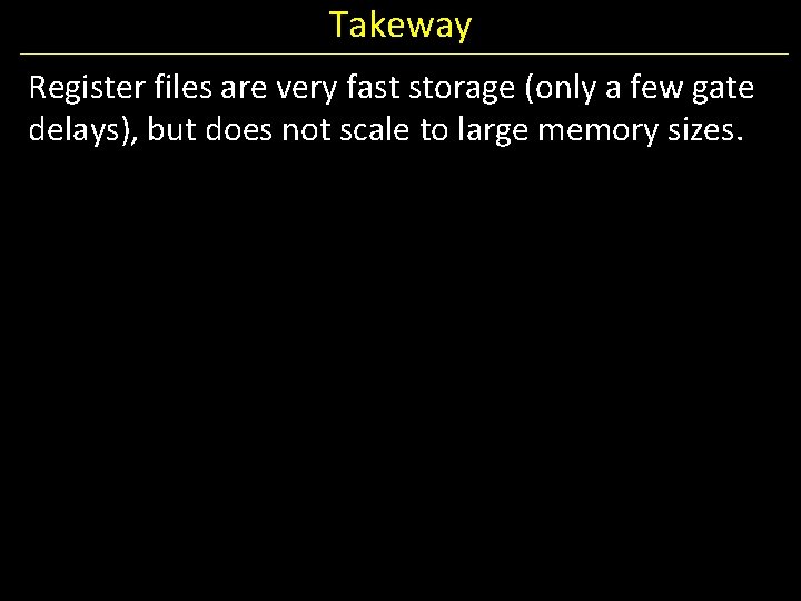
Takeway Register files are very fast storage (only a few gate delays), but does not scale to large memory sizes.

Goals for today Memory • • CPU: Register Files (i. e. Memory w/in the CPU) Scaling Memory: Tri-state devices Cache: SRAM (Static RAM—random access memory) Memory: DRAM (Dynamic RAM)

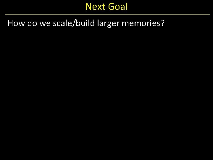
Next Goal How do we scale/build larger memories?

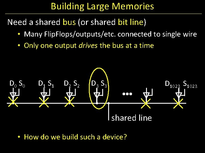
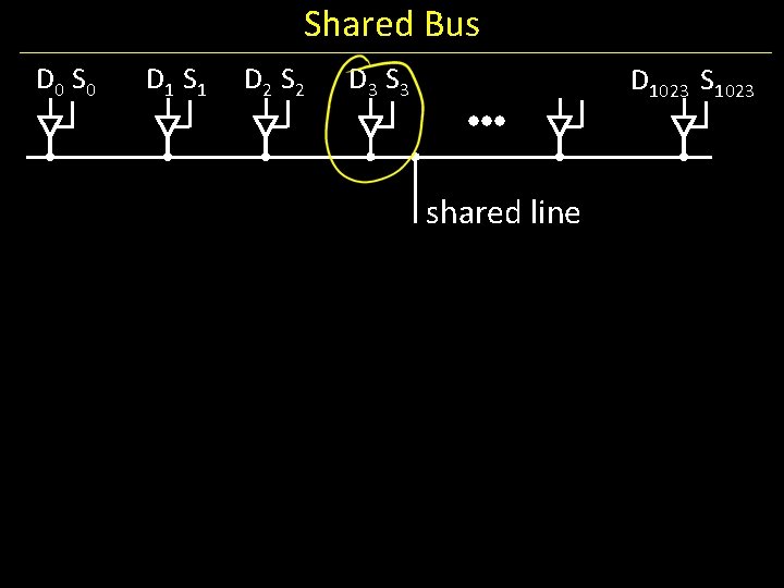
Building Large Memories Need a shared bus (or shared bit line) • Many Flip. Flops/outputs/etc. connected to single wire • Only one output drives the bus at a time D 0 S 0 D 1 S 1 D 2 S 2 D 3 S 3 D 1023 S 1023 shared line • How do we build such a device?

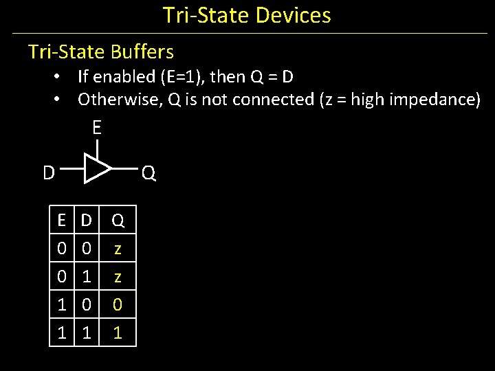
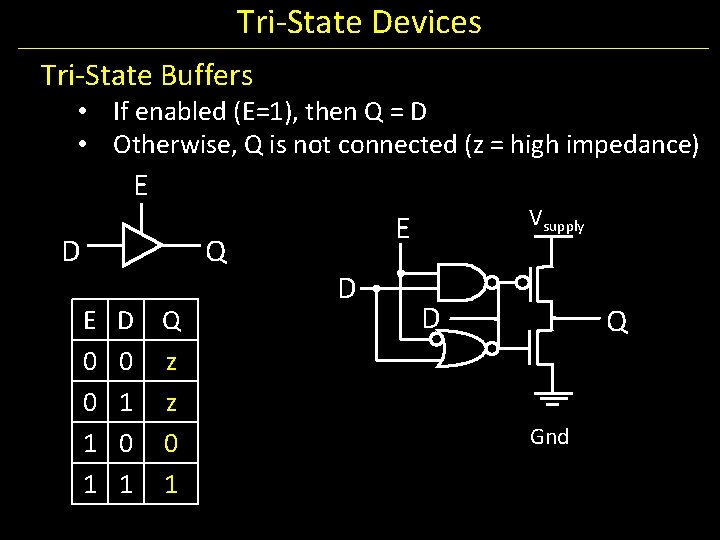
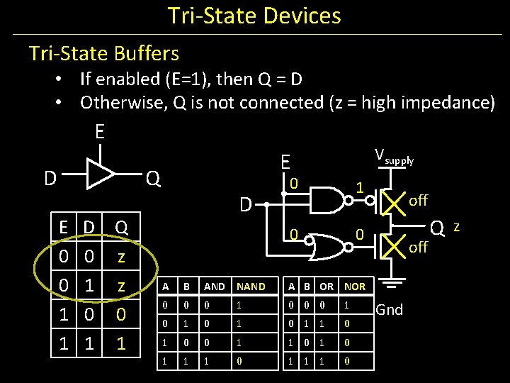
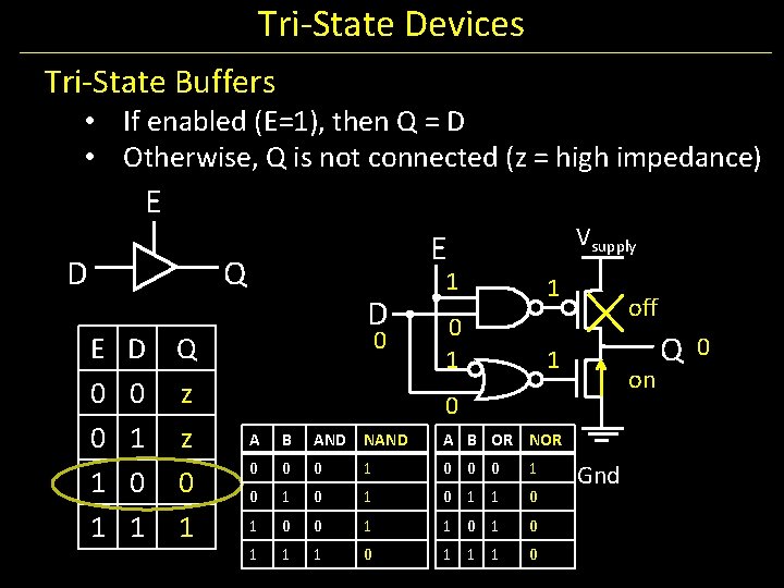
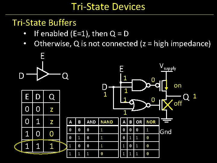
Tri-State Devices Tri-State Buffers • If enabled (E=1), then Q = D • Otherwise, Q is not connected (z = high impedance) E D Q E 0 0 1 1 D Q 0 z 1 z 0 0 1 1

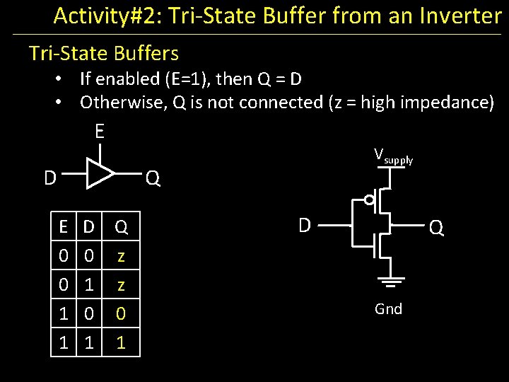
Activity#2: Tri-State Buffer from an Inverter Tri-State Buffers • If enabled (E=1), then Q = D • Otherwise, Q is not connected (z = high impedance) E D Vsupply Q E 0 0 1 1 D Q 0 z 1 z 0 0 1 1 D Q Gnd

Tri-State Devices Tri-State Buffers • If enabled (E=1), then Q = D • Otherwise, Q is not connected (z = high impedance) E D Q E 0 0 1 1 D Q 0 z 1 z 0 0 1 1 Vsupply E D D Q Gnd

Tri-State Devices Tri-State Buffers • If enabled (E=1), then Q = D • Otherwise, Q is not connected (z = high impedance) E D Q E 0 0 1 1 D Q 0 z 1 z 0 0 1 1 Vsupply E D 0 1 0 0 A B AND NAND A B OR NOR 0 0 0 1 0 1 0 1 1 1 0 off Gnd Q z

Tri-State Devices Tri-State Buffers • If enabled (E=1), then Q = D • Otherwise, Q is not connected (z = high impedance) E D Q E 0 0 1 1 D Q 0 z 1 z 0 0 1 1 Vsupply E D 0 1 1 off on 0 A B AND NAND A B OR NOR 0 0 0 1 0 1 0 1 1 1 0 Gnd Q 0

Tri-State Devices Tri-State Buffers • If enabled (E=1), then Q = D • Otherwise, Q is not connected (z = high impedance) E D Q E 0 0 1 1 D Q 0 z 1 z 0 0 1 1 Vsupply E D 1 1 0 on off 1 A B AND NAND A B OR NOR 0 0 0 1 0 1 0 1 1 1 0 Gnd Q 1

Shared Bus D 0 S 0 D 1 S 1 D 2 S 2 D 3 S 3 D 1023 S 1023 shared line

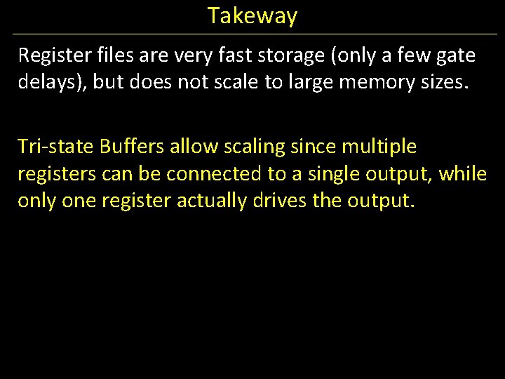
Takeway Register files are very fast storage (only a few gate delays), but does not scale to large memory sizes. Tri-state Buffers allow scaling since multiple registers can be connected to a single output, while only one register actually drives the output.

Goals for today Memory • • CPU: Register Files (i. e. Memory w/in the CPU) Scaling Memory: Tri-state devices Cache: SRAM (Static RAM—random access memory) Memory: DRAM (Dynamic RAM)

Next Goal How do we build large memories? Use similar designs as Tri-state Buffers to connect multiple registers to output line. Only one register will drive output line.

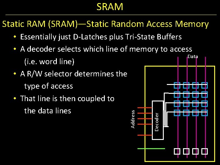
SRAM Static RAM (SRAM)—Static Random Access Memory Decoder Address • Essentially just D-Latches plus Tri-State Buffers • A decoder selects which line of memory to access Data (i. e. word line) • A R/W selector determines the type of access • That line is then coupled to the data lines

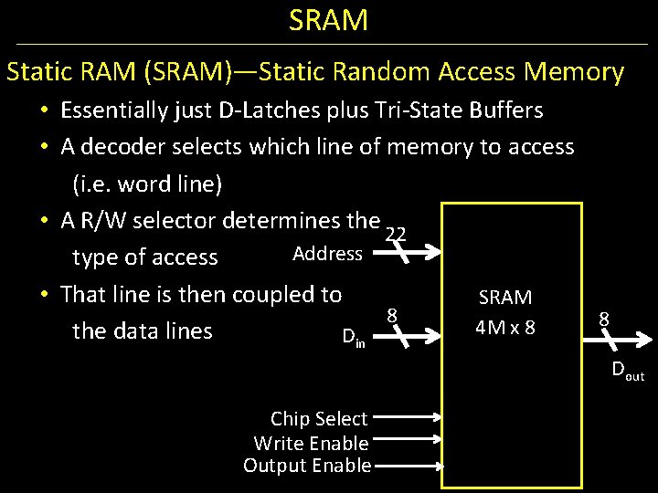
SRAM Static RAM (SRAM)—Static Random Access Memory • Essentially just D-Latches plus Tri-State Buffers • A decoder selects which line of memory to access (i. e. word line) • A R/W selector determines the 22 Address type of access • That line is then coupled to SRAM 8 8 4 M x 8 the data lines Din Dout Chip Select Write Enable Output Enable
![SRAM Din1 E g How do we design a 4 x 2 SRAM Module SRAM Din[1] E. g. How do we design a 4 x 2 SRAM Module?](https://slidetodoc.com/presentation_image_h2/6e2894c6b22b6fe3d9645b079869da55/image-52.jpg)
SRAM Din[1] E. g. How do we design a 4 x 2 SRAM Module? 0 (i. e. 4 word lines that are each 2 bits wide)? Address 2 -to-4 decoder 1 2 D Q D Q enable D Q 4 x 2 SRAM 2 Write Enable Output Enable Din[2] 3 D Q enable Dout[1] Dout[2]
![SRAM Din1 E g How do we design a 4 x 2 SRAM Module SRAM Din[1] E. g. How do we design a 4 x 2 SRAM Module?](https://slidetodoc.com/presentation_image_h2/6e2894c6b22b6fe3d9645b079869da55/image-53.jpg)
SRAM Din[1] E. g. How do we design a 4 x 2 SRAM Module? 0 (i. e. 4 word lines that are each 2 bits wide)? Address 2 -to-4 decoder 1 2 2 Write Enable Output Enable 3 Din[2] D Q D Q enable enable Dout[1] Dout[2]
![SRAM E g How do we design a 4 x 2 SRAM Module Din1 SRAM E. g. How do we design a 4 x 2 SRAM Module? Din[1]](https://slidetodoc.com/presentation_image_h2/6e2894c6b22b6fe3d9645b079869da55/image-54.jpg)
SRAM E. g. How do we design a 4 x 2 SRAM Module? Din[1] Word line 0 (i. e. 4 word lines that are each 2 bits wide)? Address 2 -to-4 decoder 1 2 2 Write Enable Output Enable Bit line 3 Din[2] D Q D Q enable enable Dout[1] Dout[2]

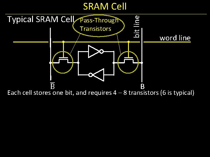
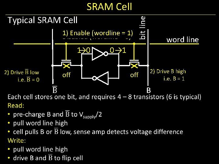
Typical SRAM Cell Pass-Through Transistors bit line SRAM Cell B word line Each cell stores one bit, and requires 4 – 8 transistors (6 is typical)

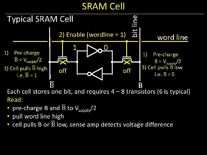
Typical SRAM Cell 2) Enable(wordline==0) 1) Disabled 1 on off bit line SRAM Cell 0 on off word line 1) Pre-charge B = Vsupply/2 3) Cell pulls B low i. e. B = 0 B

Typical SRAM Cell 1) Enable(wordline==0) 1) Disabled 1→ 0 on off bit line SRAM Cell word line 0 → 1 on off 2) Drive B high i. e. B = 1 B
![SRAM E g How do we design a 4 x 2 SRAM Module Din1 SRAM E. g. How do we design a 4 x 2 SRAM Module? Din[1]](https://slidetodoc.com/presentation_image_h2/6e2894c6b22b6fe3d9645b079869da55/image-58.jpg)
SRAM E. g. How do we design a 4 x 2 SRAM Module? Din[1] Word line 0 (i. e. 4 word lines that are each 2 bits wide)? Address 2 -to-4 decoder 1 2 2 Write Enable Output Enable Bit line 3 Din[2] D Q D Q enable enable Dout[1] Dout[2]
![SRAM Din1 E g How do we design a 4 x 2 SRAM Module SRAM Din[1] E. g. How do we design a 4 x 2 SRAM Module?](https://slidetodoc.com/presentation_image_h2/6e2894c6b22b6fe3d9645b079869da55/image-59.jpg)
SRAM Din[1] E. g. How do we design a 4 x 2 SRAM Module? 0 (i. e. 4 word lines that are each 2 bits wide)? Address 2 -to-4 decoder 1 2 D Q D Q enable D Q 4 x 2 SRAM 2 Write Enable Output Enable Din[2] 3 D Q enable Dout[1] Dout[2]

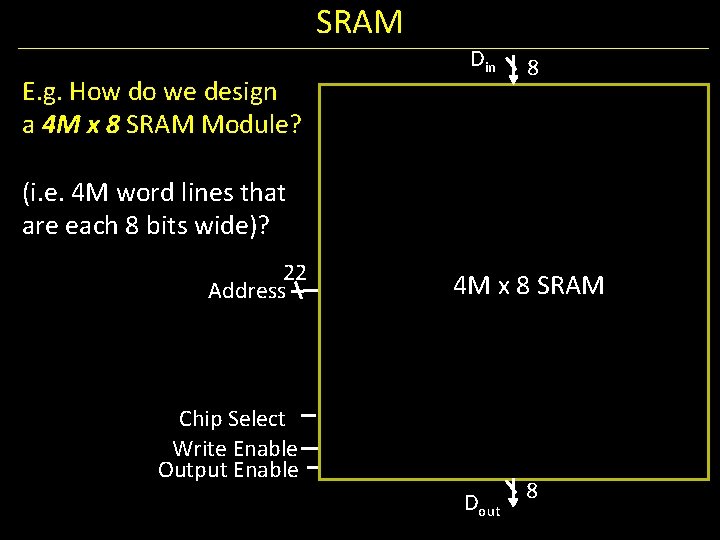
SRAM E. g. How do we design a 4 M x 8 SRAM Module? Din 8 (i. e. 4 M word lines that are each 8 bits wide)? 22 Address 4 M x 8 SRAM Chip Select Write Enable Output Enable Dout 8

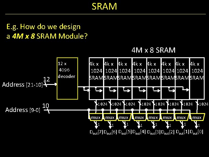
SRAM E. g. How do we design a 4 M x 8 SRAM Module? 4 M x 8 SRAM Address [21 -10] Address [9 -0] 12 10 12 x 4096 decoder 4 k x 4 k x 1024 1024 SRAMSRAM 1024 mux mux 1 1024 1024 mux mux mux 1 1 1 Dout[7]Dout[6] Dout[5]Dout[4] Dout[3]Dout[2] Dout[1]Dout[0]

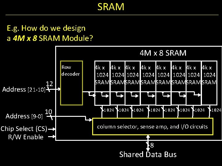
SRAM E. g. How do we design a 4 M x 8 SRAM Module? 4 M x 8 SRAM Row decoder Address [21 -10] Address [9 -0] 12 10 Chip Select (CS) R/W Enable 4 k x 4 k x 1024 1024 SRAMSRAM 1024 1024 column selector, sense amp, and I/O circuits 8 Shared Data Bus 1024

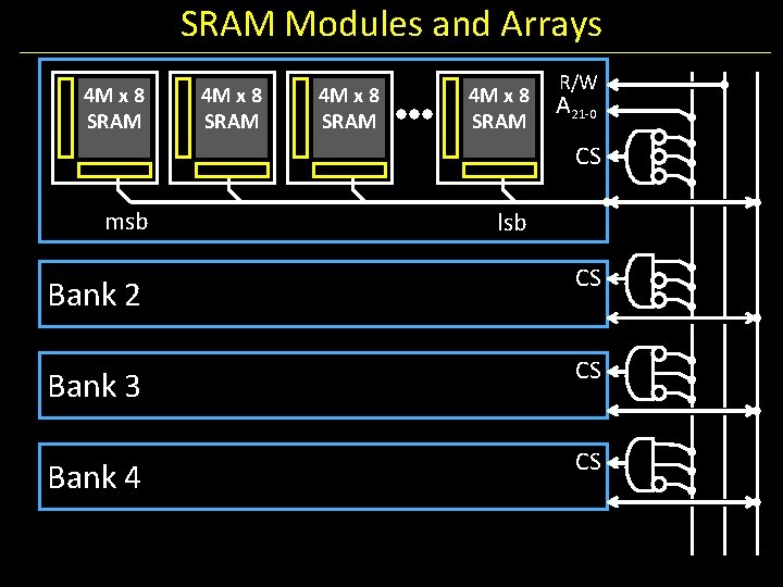
SRAM Modules and Arrays 4 M x 8 SRAM R/W A 21 -0 CS msb lsb Bank 2 CS Bank 3 CS Bank 4 CS

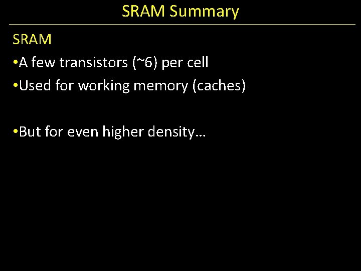
SRAM Summary SRAM • A few transistors (~6) per cell • Used for working memory (caches) • But for even higher density…

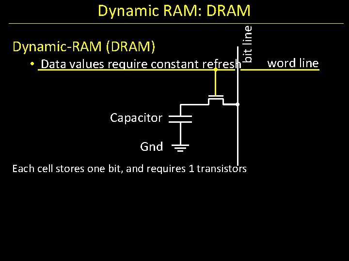
Dynamic-RAM (DRAM) bit line Dynamic RAM: DRAM • Data values require constant refresh Capacitor Gnd Each cell stores one bit, and requires 1 transistors word line

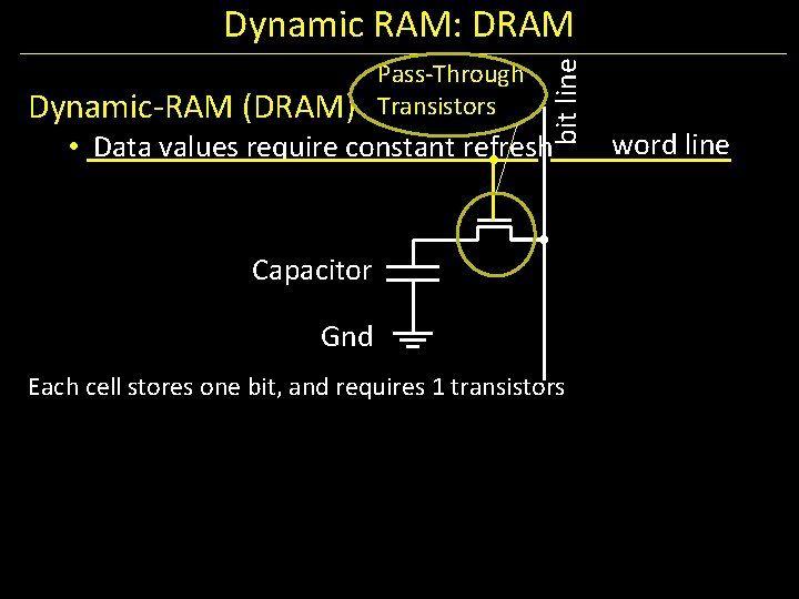
Dynamic-RAM (DRAM) Pass-Through Transistors bit line Dynamic RAM: DRAM • Data values require constant refresh Capacitor Gnd Each cell stores one bit, and requires 1 transistors word line

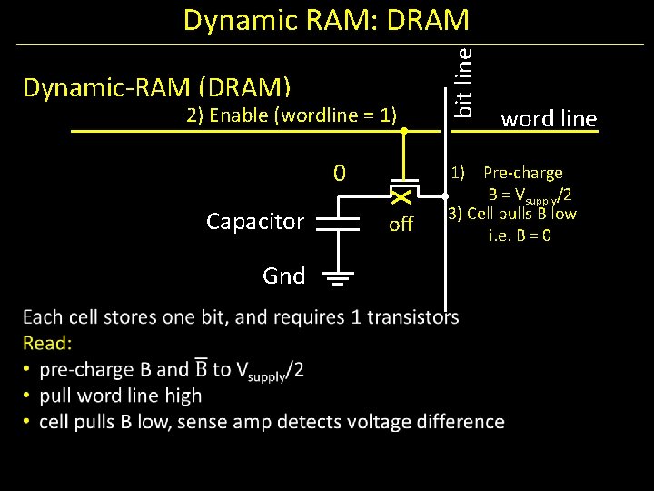
Dynamic-RAM (DRAM) Disabled 2) Enable(wordline==0) 1) 0 Capacitor Gnd off on bit line Dynamic RAM: DRAM word line 1) Pre-charge B = Vsupply/2 3) Cell pulls B low i. e. B = 0

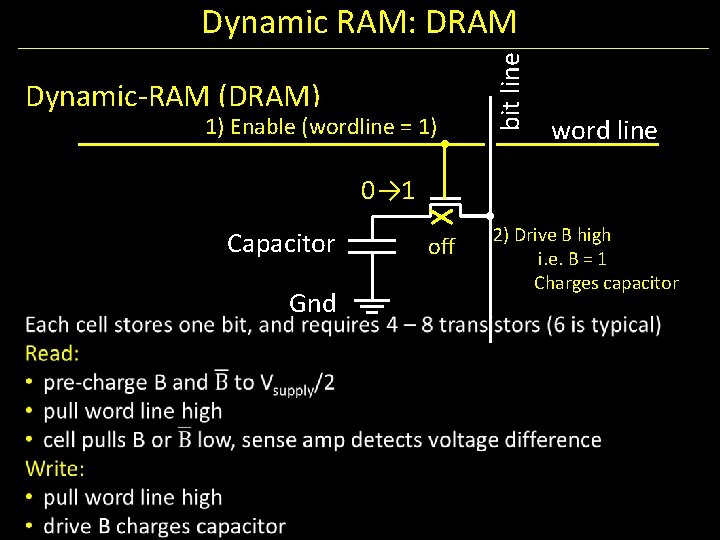
Dynamic-RAM (DRAM) Disabled 1) Enable(wordline==0) 1) bit line Dynamic RAM: DRAM word line 0 → 1 Capacitor Gnd on off 2) Drive B high i. e. B = 1 Charges capacitor

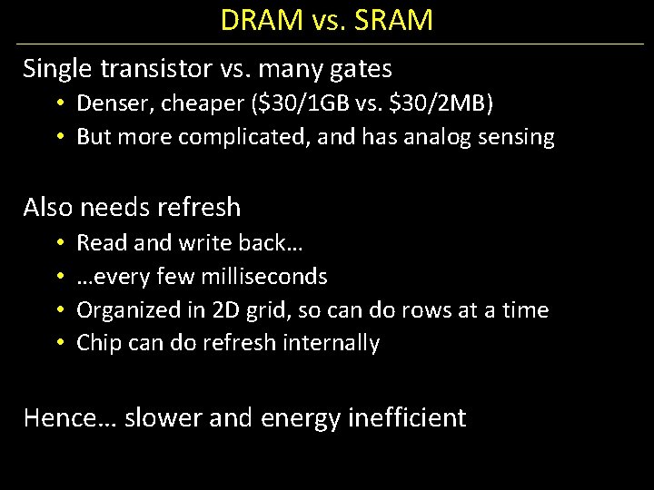
DRAM vs. SRAM Single transistor vs. many gates • Denser, cheaper ($30/1 GB vs. $30/2 MB) • But more complicated, and has analog sensing Also needs refresh • • Read and write back… …every few milliseconds Organized in 2 D grid, so can do rows at a time Chip can do refresh internally Hence… slower and energy inefficient

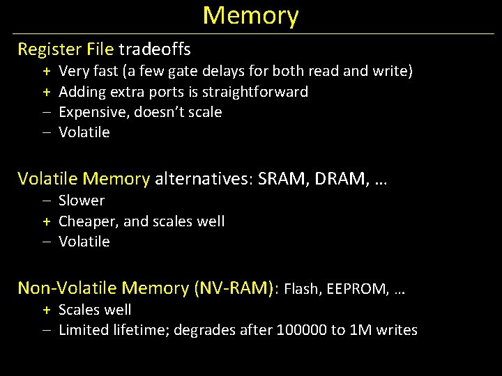
Memory Register File tradeoffs + + – – Very fast (a few gate delays for both read and write) Adding extra ports is straightforward Expensive, doesn’t scale Volatile Memory alternatives: SRAM, DRAM, … – Slower + Cheaper, and scales well – Volatile Non-Volatile Memory (NV-RAM): Flash, EEPROM, … + Scales well – Limited lifetime; degrades after 100000 to 1 M writes

Summary We now have enough building blocks to build machines that can perform non-trivial computational tasks Register File: Tens of words of working memory SRAM: Millions of words of working memory DRAM: Billions of words of working memory NVRAM: long term storage (usb fob, solid state disks, BIOS, …) Next time we will build a simple processor!