Memory Prof Hakim Weatherspoon CS 3410 Spring 2015



- Slides: 38

Memory Prof. Hakim Weatherspoon CS 3410, Spring 2015 Computer Science Cornell University See P&H Appendix B. 8 (register files) and B. 9

Announcements Make sure to go to your Lab Section this week Completed Lab 1 due before winter break, Friday, Feb 13 th Note, a Design Document is due when you submit Lab 1 final circuit Work alone Save your work! • Save often. Verify file is non-zero. Periodically save to Dropbox, email. • Beware of Mac. OSX 10. 5 (leopard) and 10. 6 (snow-leopard) Homework 1 is out Due a week before prelim 1, Monday, February 23 rd Work on problems incrementally, as we cover them in lecture (i. e. part 1) Office Hours for help Work alone, BUT use your resources • Lab Section, Piazza. com, Office Hours • Class notes, book, Sections, CSUGLab

Announcements Check online syllabus/schedule • http: //www. cs. cornell. edu/Courses/CS 3410/2015 sp/schedule. html • • • Slides and Reading for lectures Office Hours Pictures of all TAs Homework and Programming Assignments Dates to keep in Mind • • Prelims: Tue Mar 3 rd and Thur April 30 th Lab 1: Due next Friday, Feb 13 th before Winter break Proj 2: Due Thur Mar 26 th before Spring break Final Project: Due when final would be (not known until Feb 14 th Schedule is subject to change

Collaboration, Late, Re-grading Policies “Black Board” Collaboration Policy • Can discuss approach together on a “black board” • Leave and write up solution independently • Do not copy solutions Late Policy • Each person has a total of four “slip days” • Max of two slip days for any individual assignment • Slip days deducted first for any late assignment, cannot selectively apply slip days • For projects, slip days are deducted from all partners • 25% deducted per day late after slip days are exhausted Regrade policy • Submit written request to lead TA, and lead TA will pick a different grader • Submit another written request, lead TA will regrade directly • Submit yet another written request for professor to regrade.

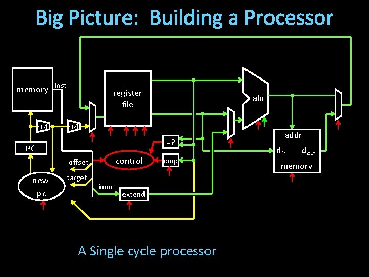
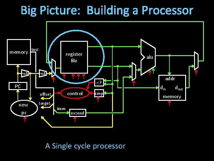
Big Picture: Building a Processor memory inst +4 register file +4 =? PC control offset new pc alu target imm cmp extend A Single cycle processor addr din dout memory

Goals for today Memory • • Register Files Tri-state devices SRAM (Static RAM—random access memory) DRAM (Dynamic RAM)

Big Picture: Building a Processor memory inst +4 register file +4 =? PC control offset new pc alu target imm cmp extend A Single cycle processor addr din dout memory

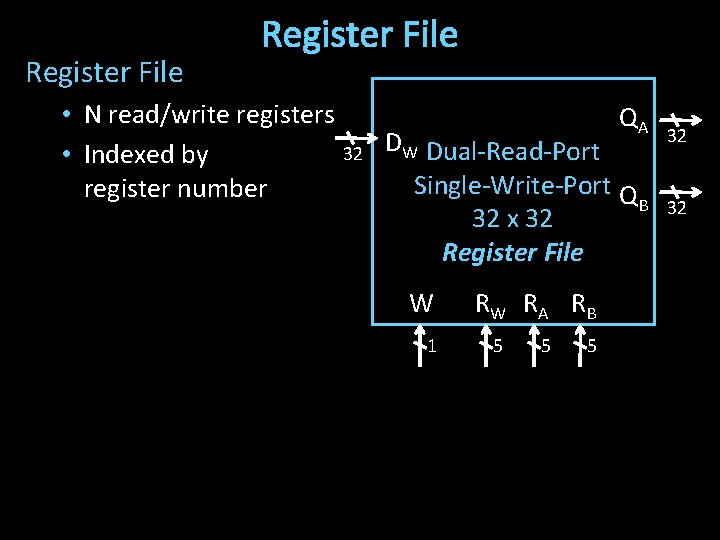
Register File • N read/write registers QA 32 DW Dual-Read-Port • Indexed by Single-Write-Port Q register number B 32 x 32 Register File W 1 RW RA RB 5 5 5 32 32

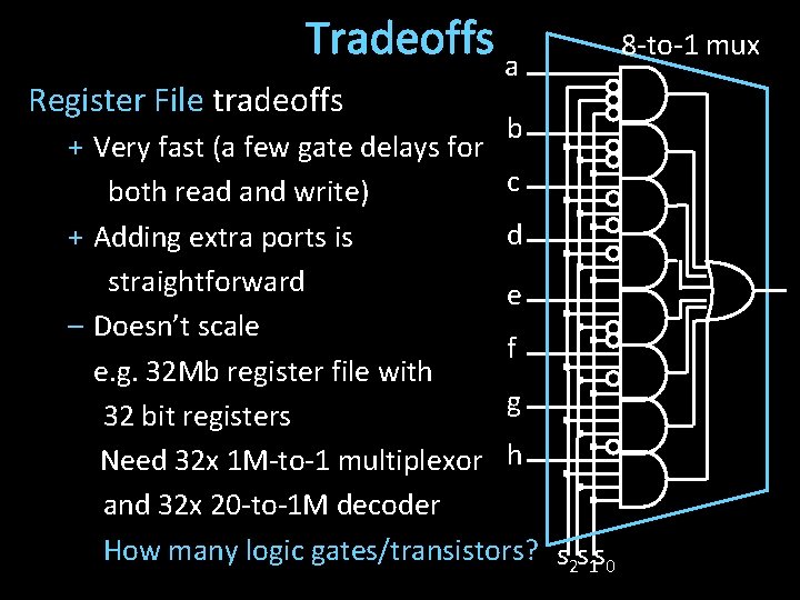
Tradeoffs a Register File tradeoffs b + Very fast (a few gate delays for c both read and write) d + Adding extra ports is straightforward e – Doesn’t scale f e. g. 32 Mb register file with g 32 bit registers Need 32 x 1 M-to-1 multiplexor h and 32 x 20 -to-1 M decoder How many logic gates/transistors? s 2 s 1 s 0 8 -to-1 mux

Takeway Register files are very fast storage (only a few gate delays), but does not scale to large memory sizes.

Goals for today Memory • • CPU: Register Files (i. e. Memory w/in the CPU) Scaling Memory: Tri-state devices Cache: SRAM (Static RAM—random access memory) Memory: DRAM (Dynamic RAM)

Next Goal How do we scale/build larger memories?

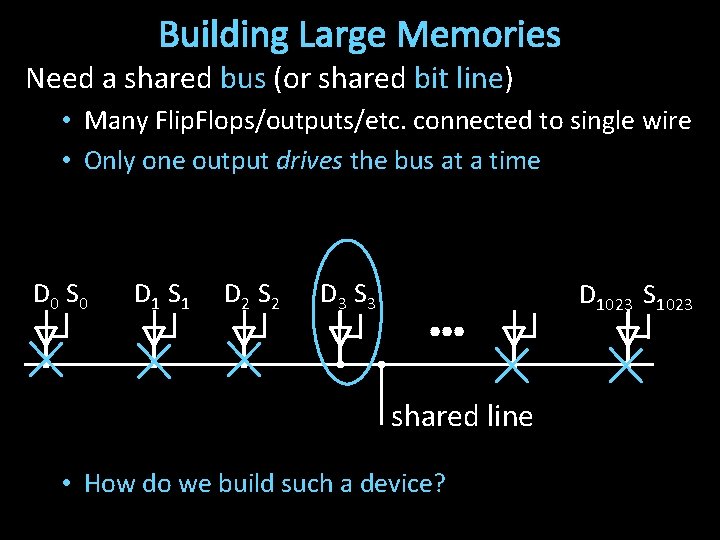
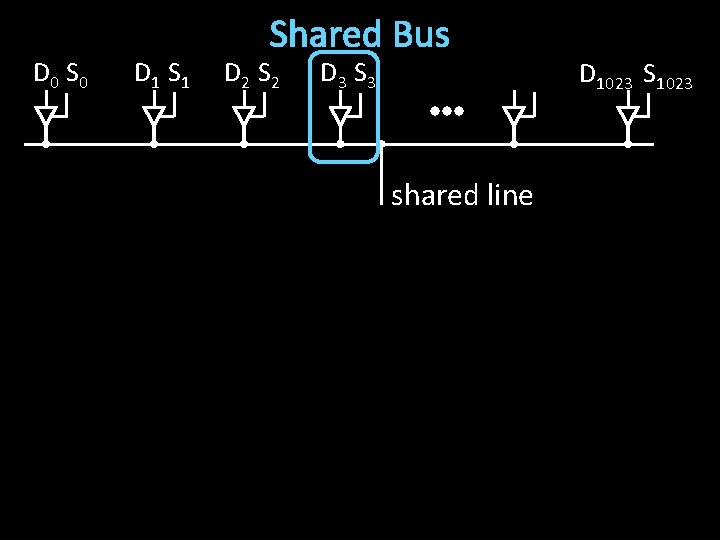
Building Large Memories Need a shared bus (or shared bit line) • Many Flip. Flops/outputs/etc. connected to single wire • Only one output drives the bus at a time D 0 S 0 D 1 S 1 D 2 S 2 D 3 S 3 D 1023 S 1023 shared line • How do we build such a device?

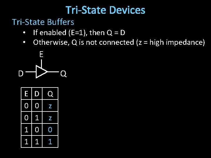
Tri-State Devices Tri-State Buffers • If enabled (E=1), then Q = D • Otherwise, Q is not connected (z = high impedance) E D Q E 0 0 1 1 D Q 0 z 1 z 0 0 1 1

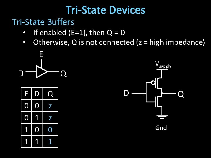
Tri-State Devices Tri-State Buffers • If enabled (E=1), then Q = D • Otherwise, Q is not connected (z = high impedance) E D Vsupply Q E 0 0 1 1 D Q 0 z 1 z 0 0 1 1 D Q Gnd

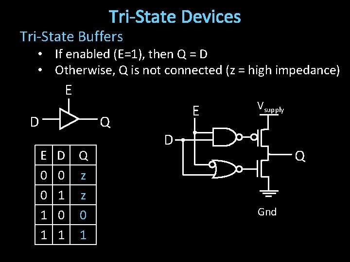
Tri-State Devices Tri-State Buffers • If enabled (E=1), then Q = D • Otherwise, Q is not connected (z = high impedance) E D Q E 0 0 1 1 D Q 0 z 1 z 0 0 1 1 E Vsupply D Q Gnd

D 0 S 0 D 1 Shared Bus D 2 S 2 D 3 S 3 shared line D 1023 S 1023

Takeway Register files are very fast storage (only a few gate delays), but does not scale to large memory sizes. Tri-state Buffers allow scaling since multiple registers can be connected to a single output, while only one register actually drives the output.

Goals for today Memory • • CPU: Register Files (i. e. Memory w/in the CPU) Scaling Memory: Tri-state devices Cache: SRAM (Static RAM—random access memory) Memory: DRAM (Dynamic RAM)

Next Goal How do we build large memories? Use similar designs as Tri-state Buffers to connect multiple registers to output line. Only one register will drive output line.

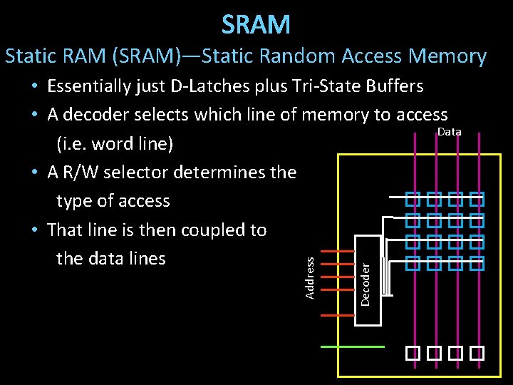
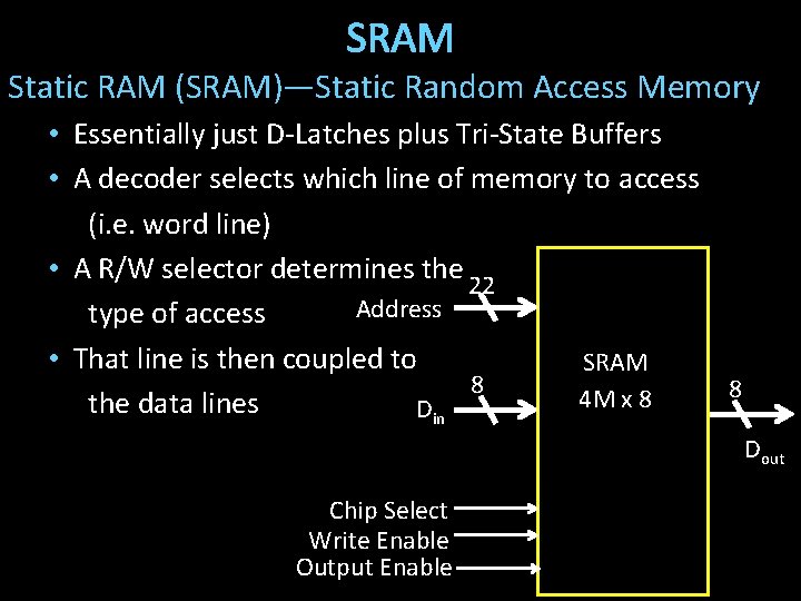
SRAM Static RAM (SRAM)—Static Random Access Memory Decoder Address • Essentially just D-Latches plus Tri-State Buffers • A decoder selects which line of memory to access Data (i. e. word line) • A R/W selector determines the type of access • That line is then coupled to the data lines

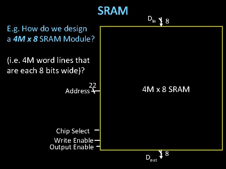
SRAM Static RAM (SRAM)—Static Random Access Memory • Essentially just D-Latches plus Tri-State Buffers • A decoder selects which line of memory to access (i. e. word line) • A R/W selector determines the 22 Address type of access • That line is then coupled to SRAM 8 8 4 M x 8 the data lines Din Dout Chip Select Write Enable Output Enable

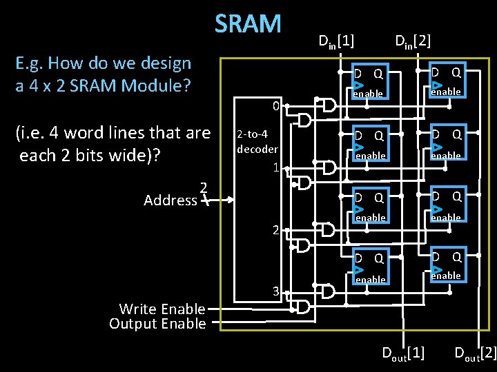
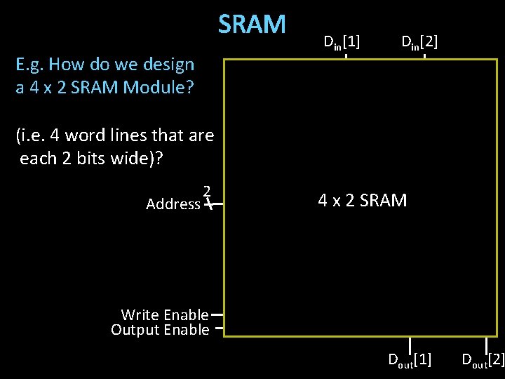
SRAM E. g. How do we design a 4 x 2 SRAM Module? 0 (i. e. 4 word lines that are each 2 bits wide)? Address 2 -to-4 decoder 1 2 Din[2] D Q D Q enable D Q 4 x 2 SRAM 2 Write Enable Output Enable Din[1] 3 D Q enable Dout[1] Dout[2]

SRAM E. g. How do we design a 4 x 2 SRAM Module? 0 (i. e. 4 word lines that are each 2 bits wide)? Address 2 -to-4 decoder 1 2 2 Write Enable Output Enable 3 Din[1] Din[2] D Q D Q enable enable Dout[1] Dout[2]

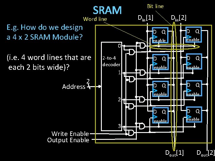
SRAM E. g. How do we design a 4 x 2 SRAM Module? Word line 0 (i. e. 4 word lines that are each 2 bits wide)? Address 2 -to-4 decoder 1 2 2 Write Enable Output Enable 3 Bit line Din[1] Din[2] D Q D Q enable enable Dout[1] Dout[2]

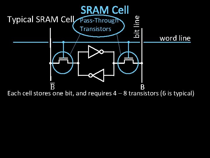
Pass-Through Transistors bit line Typical SRAM Cell B word line Each cell stores one bit, and requires 4 – 8 transistors (6 is typical)

SRAM E. g. How do we design a 4 x 2 SRAM Module? Word line 0 (i. e. 4 word lines that are each 2 bits wide)? Address 2 -to-4 decoder 1 2 2 Write Enable Output Enable 3 Bit line Din[1] Din[2] D Q D Q enable enable Dout[1] Dout[2]

SRAM E. g. How do we design a 4 x 2 SRAM Module? 0 (i. e. 4 word lines that are each 2 bits wide)? Address 2 -to-4 decoder 1 2 Din[2] D Q D Q enable D Q 4 x 2 SRAM 2 Write Enable Output Enable Din[1] 3 D Q enable Dout[1] Dout[2]

SRAM E. g. How do we design a 4 M x 8 SRAM Module? Din 8 (i. e. 4 M word lines that are each 8 bits wide)? 22 Address 4 M x 8 SRAM Chip Select Write Enable Output Enable Dout 8

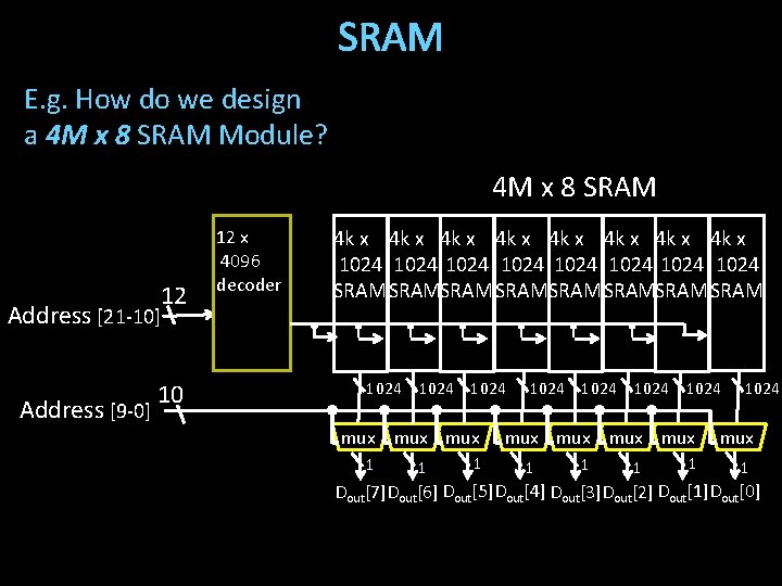
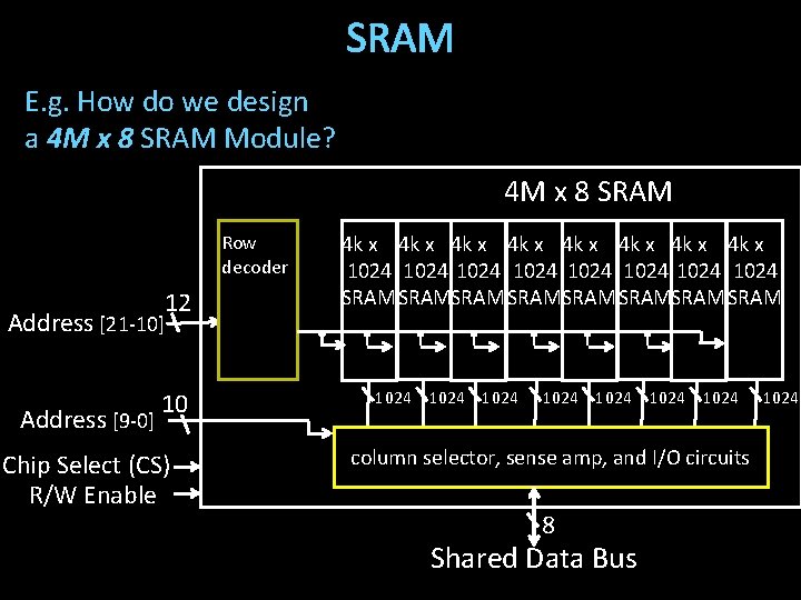
SRAM E. g. How do we design a 4 M x 8 SRAM Module? 4 M x 8 SRAM Address [21 -10] Address [9 -0] 12 10 12 x 4096 decoder 4 k x 4 k x 1024 1024 SRAMSRAM 1024 mux mux 1 1024 1024 mux mux mux 1 1 1 Dout[7]Dout[6] Dout[5]Dout[4] Dout[3]Dout[2] Dout[1]Dout[0]

SRAM E. g. How do we design a 4 M x 8 SRAM Module? 4 M x 8 SRAM Row decoder Address [21 -10] Address [9 -0] 12 10 Chip Select (CS) R/W Enable 4 k x 4 k x 1024 1024 SRAMSRAM 1024 1024 column selector, sense amp, and I/O circuits 8 Shared Data Bus 1024

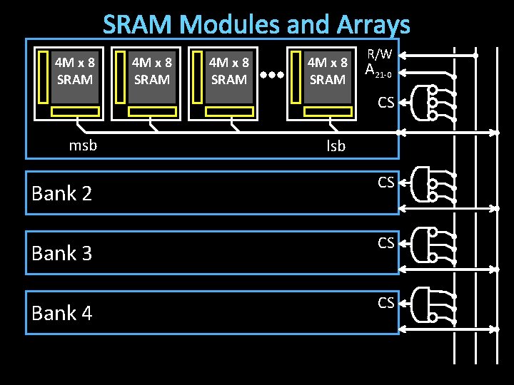
SRAM Modules and Arrays 4 M x 8 SRAM R/W A 21 -0 CS msb lsb Bank 2 CS Bank 3 CS Bank 4 CS

SRAM Summary SRAM • A few transistors (~6) per cell • Used for working memory (caches) • But for even higher density…

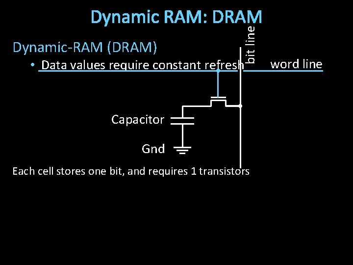
Dynamic-RAM (DRAM) bit line Dynamic RAM: DRAM • Data values require constant refresh Capacitor Gnd Each cell stores one bit, and requires 1 transistors word line

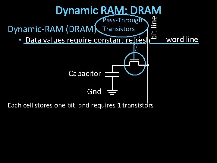
Dynamic-RAM (DRAM) Pass-Through Transistors bit line Dynamic RAM: DRAM • Data values require constant refresh Capacitor Gnd Each cell stores one bit, and requires 1 transistors word line

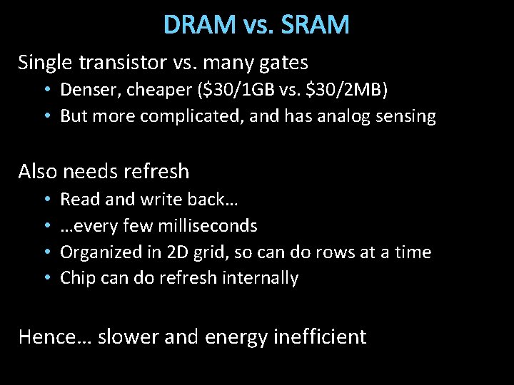
DRAM vs. SRAM Single transistor vs. many gates • Denser, cheaper ($30/1 GB vs. $30/2 MB) • But more complicated, and has analog sensing Also needs refresh • • Read and write back… …every few milliseconds Organized in 2 D grid, so can do rows at a time Chip can do refresh internally Hence… slower and energy inefficient

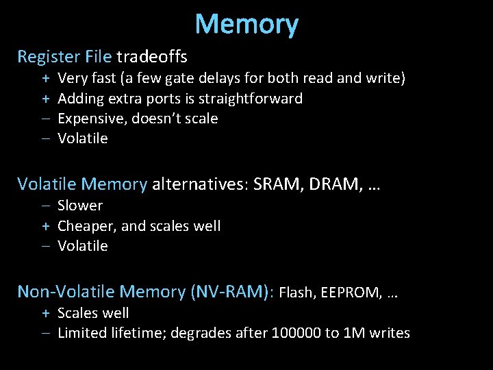
Memory Register File tradeoffs + + – – Very fast (a few gate delays for both read and write) Adding extra ports is straightforward Expensive, doesn’t scale Volatile Memory alternatives: SRAM, DRAM, … – Slower + Cheaper, and scales well – Volatile Non-Volatile Memory (NV-RAM): Flash, EEPROM, … + Scales well – Limited lifetime; degrades after 100000 to 1 M writes

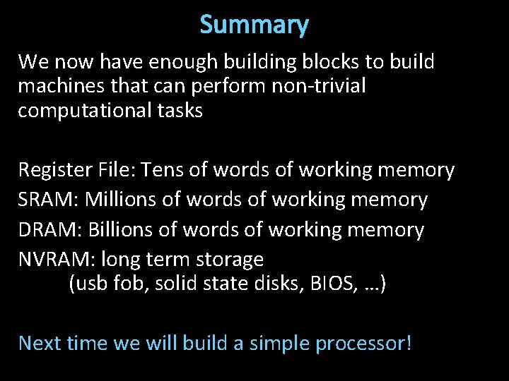
Summary We now have enough building blocks to build machines that can perform non-trivial computational tasks Register File: Tens of words of working memory SRAM: Millions of words of working memory DRAM: Billions of words of working memory NVRAM: long term storage (usb fob, solid state disks, BIOS, …) Next time we will build a simple processor!