Lecture 5 DC Transient Response Outline q q



- Slides: 74
Lecture 5: DC & Transient Response
Outline q q q Pass Transistors DC Response Logic Levels and Noise Margins Transient Response RC Delay Models Delay Estimation 5: DC and Transient Response CMOS VLSI Design 4 th Ed. 2
Pass Transistors q We have assumed source is grounded q What if source > 0? – e. g. pass transistor passing VDD q Vg = VDD – If Vs > VDD-Vt, Vgs < Vt – Hence transistor would turn itself off q n. MOS pass transistors pull no higher than VDD-Vtn – Called a degraded “ 1” – Approach degraded value slowly (low Ids) q p. MOS pass transistors pull no lower than Vtp q Transmission gates are needed to pass both 0 and 1 5: DC and Transient Response CMOS VLSI Design 4 th Ed. 3
Pass Transistor Ckts 5: DC and Transient Response CMOS VLSI Design 4 th Ed. 4
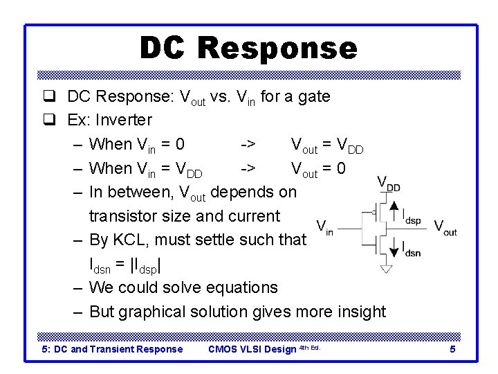
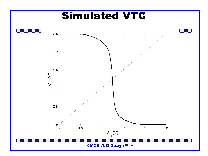
DC Response q DC Response: Vout vs. Vin for a gate q Ex: Inverter – When Vin = 0 -> Vout = VDD – When Vin = VDD -> Vout = 0 – In between, Vout depends on transistor size and current – By KCL, must settle such that Idsn = |Idsp| – We could solve equations – But graphical solution gives more insight 5: DC and Transient Response CMOS VLSI Design 4 th Ed. 5
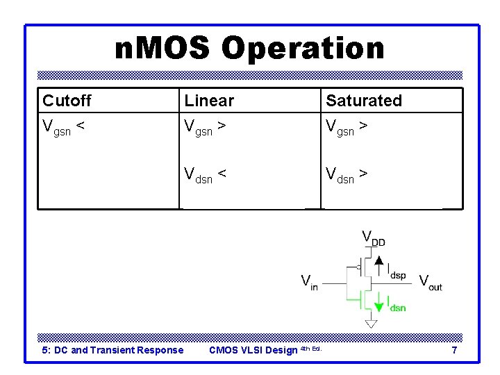
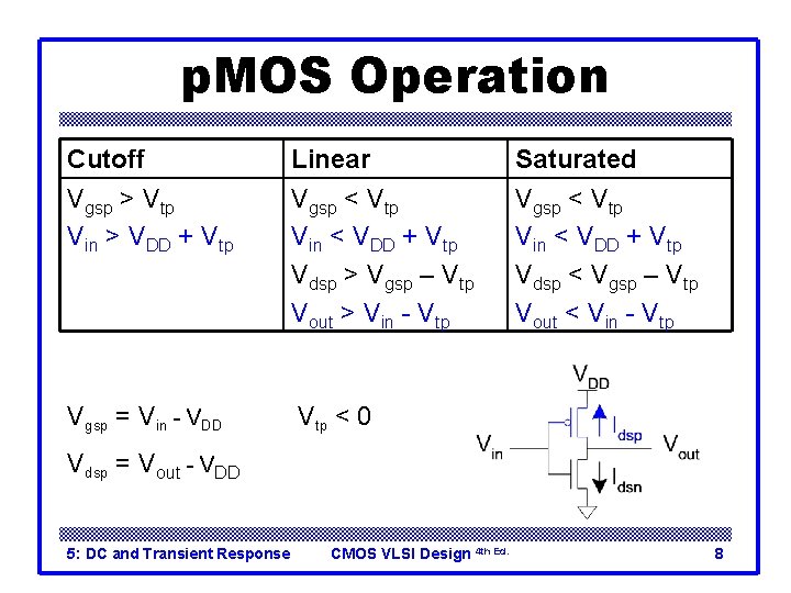
Transistor Operation q Current depends on region of transistor behavior q For what Vin and Vout are n. MOS and p. MOS in – Cutoff? – Linear? – Saturation? 5: DC and Transient Response CMOS VLSI Design 4 th Ed. 6
n. MOS Operation Cutoff Vgsn < Vtn Vin < Vtn Linear Vgsn > Vtn Vin > Vtn Vdsn < Vgsn – Vtn Vout < Vin - Vtn Saturated Vgsn > Vtn Vin > Vtn Vdsn > Vgsn – Vtn Vout > Vin - Vtn Vgsn = Vin Vdsn = Vout 5: DC and Transient Response CMOS VLSI Design 4 th Ed. 7
p. MOS Operation Cutoff Vgsp > Vtp Vin > VDD + Vtp Linear Vgsp < Vtp Vin < VDD + Vtp Vdsp > Vgsp – Vtp Vout > Vin - Vtp Vgsp = Vin - VDD Vtp < 0 Saturated Vgsp < Vtp Vin < VDD + Vtp Vdsp < Vgsp – Vtp Vout < Vin - Vtp Vdsp = Vout - VDD 5: DC and Transient Response CMOS VLSI Design 4 th Ed. 8
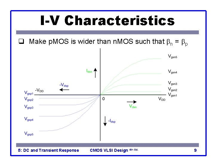
I-V Characteristics q Make p. MOS is wider than n. MOS such that bn = bp 5: DC and Transient Response CMOS VLSI Design 4 th Ed. 9
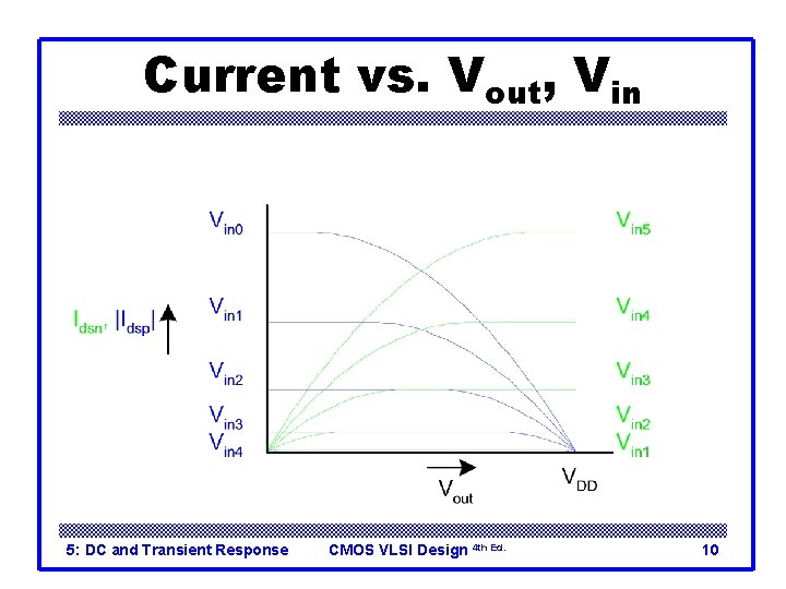
Current vs. Vout, Vin 5: DC and Transient Response CMOS VLSI Design 4 th Ed. 10
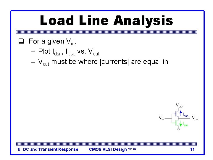
Load Line Analysis q For a given Vin: – Plot Idsn, Idsp vs. Vout – Vout must be where |currents| are equal in 5: DC and Transient Response CMOS VLSI Design 4 th Ed. 11
Load Line Analysis 0. 4 V 0. 6 V 0. 8 V. 2 V q Vin = 0 V DD DD DD 5: DC and Transient Response CMOS VLSI Design 4 th Ed. 12
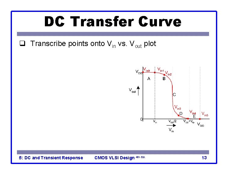
DC Transfer Curve q Transcribe points onto Vin vs. Vout plot 5: DC and Transient Response CMOS VLSI Design 4 th Ed. 13
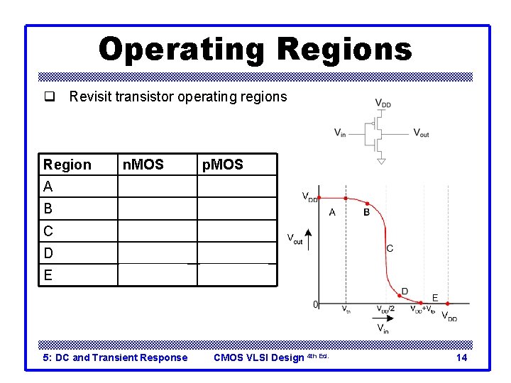
Operating Regions q Revisit transistor operating regions Region n. MOS p. MOS A Cutoff Linear B Saturation Linear C Saturation D Linear Saturation E Linear Cutoff 5: DC and Transient Response CMOS VLSI Design 4 th Ed. 14
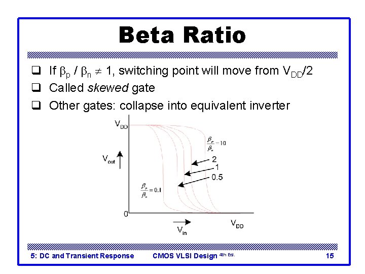
Beta Ratio q If bp / bn 1, switching point will move from VDD/2 q Called skewed gate q Other gates: collapse into equivalent inverter 5: DC and Transient Response CMOS VLSI Design 4 th Ed. 15
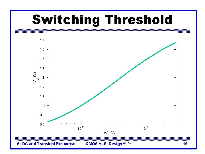
Switching Threshold 1. 8 1. 7 1. 6 1. 5 M V (V) 1. 4 1. 3 1. 2 1. 1 1 0. 9 0. 8 10 0 10 W /W p 5: DC and Transient Response 1 n CMOS VLSI Design 4 th Ed. 16
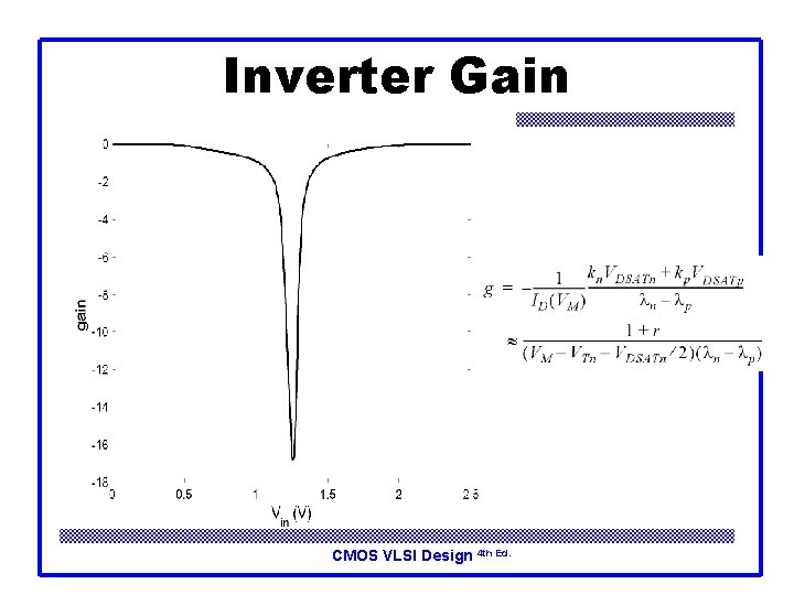
Inverter Gain CMOS VLSI Design 4 th Ed.
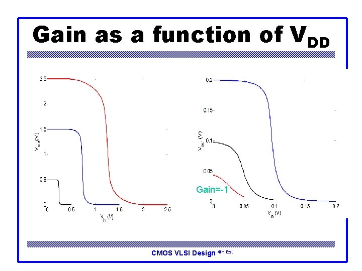
Gain as a function of VDD Gain=-1 CMOS VLSI Design 4 th Ed.
Simulated VTC CMOS VLSI Design 4 th Ed.
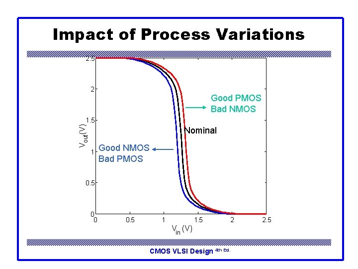
Impact of Process Variations 2. 5 2 Good PMOS Bad NMOS Vout(V) 1. 5 Nominal 1 Good NMOS Bad PMOS 0. 5 0 0 0. 5 1 1. 5 Vin (V) CMOS VLSI Design 4 th Ed. 2 2. 5
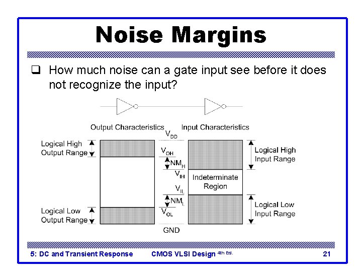
Noise Margins q How much noise can a gate input see before it does not recognize the input? 5: DC and Transient Response CMOS VLSI Design 4 th Ed. 21
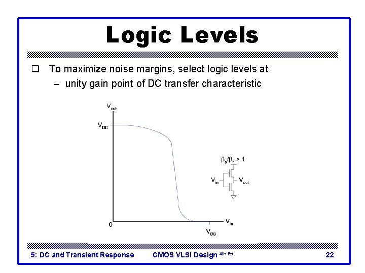
Logic Levels q To maximize noise margins, select logic levels at – unity gain point of DC transfer characteristic 5: DC and Transient Response CMOS VLSI Design 4 th Ed. 22
Transient Response q DC analysis tells us Vout if Vin is constant q Transient analysis tells us Vout(t) if Vin(t) changes – Requires solving differential equations q Input is usually considered to be a step or ramp – From 0 to VDD or vice versa 5: DC and Transient Response CMOS VLSI Design 4 th Ed. 23
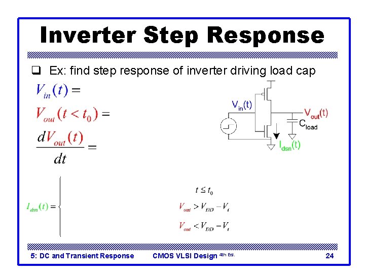
Inverter Step Response q Ex: find step response of inverter driving load cap 5: DC and Transient Response CMOS VLSI Design 4 th Ed. 24
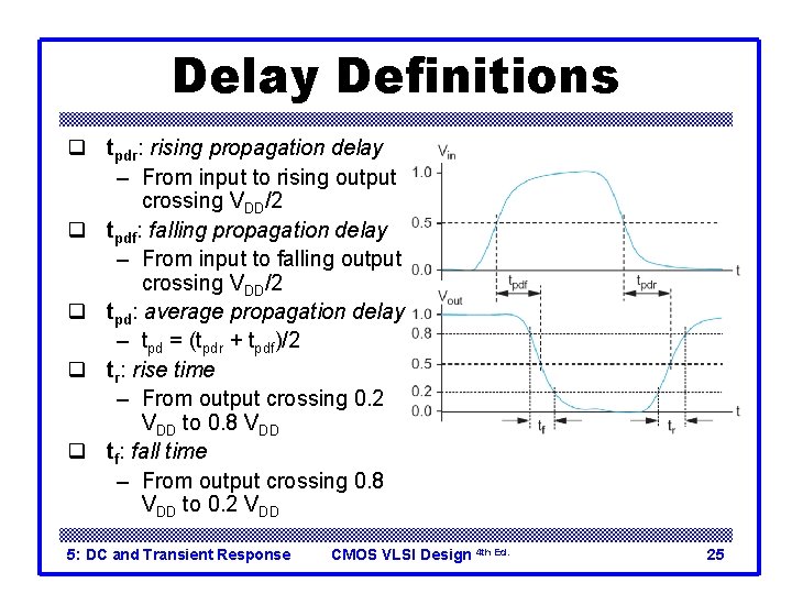
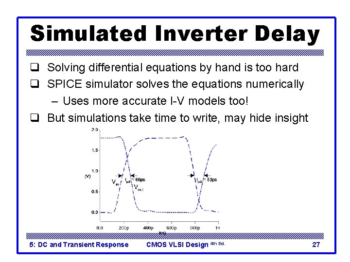
Delay Definitions q tpdr: rising propagation delay – From input to rising output crossing VDD/2 q tpdf: falling propagation delay – From input to falling output crossing VDD/2 q tpd: average propagation delay – tpd = (tpdr + tpdf)/2 q tr: rise time – From output crossing 0. 2 VDD to 0. 8 VDD q tf: fall time – From output crossing 0. 8 VDD to 0. 2 VDD 5: DC and Transient Response CMOS VLSI Design 4 th Ed. 25
Delay Definitions q tcdr: rising contamination delay – From input to rising output crossing VDD/2 q tcdf: falling contamination delay – From input to falling output crossing VDD/2 q tcd: average contamination delay – tpd = (tcdr + tcdf)/2 5: DC and Transient Response CMOS VLSI Design 4 th Ed. 26
Simulated Inverter Delay q Solving differential equations by hand is too hard q SPICE simulator solves the equations numerically – Uses more accurate I-V models too! q But simulations take time to write, may hide insight 5: DC and Transient Response CMOS VLSI Design 4 th Ed. 27
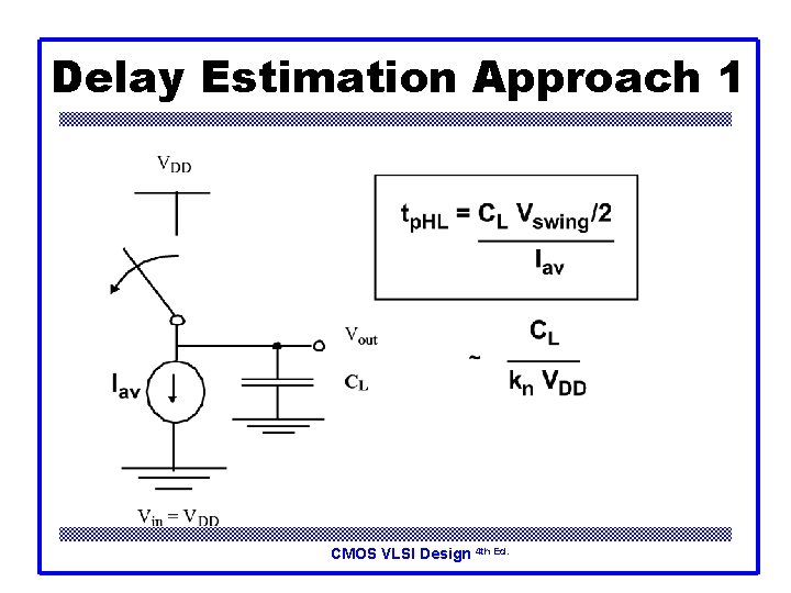
Delay Estimation Approach 1 CMOS VLSI Design 4 th Ed.
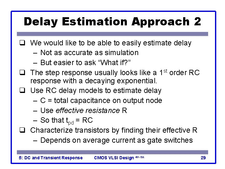
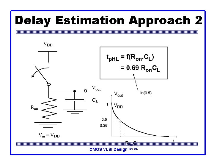
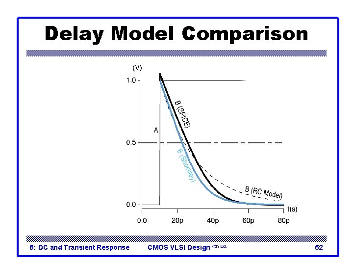
Delay Estimation Approach 2 q We would like to be able to easily estimate delay – Not as accurate as simulation – But easier to ask “What if? ” q The step response usually looks like a 1 st order RC response with a decaying exponential. q Use RC delay models to estimate delay – C = total capacitance on output node – Use effective resistance R – So that tpd = RC q Characterize transistors by finding their effective R – Depends on average current as gate switches 5: DC and Transient Response CMOS VLSI Design 4 th Ed. 29
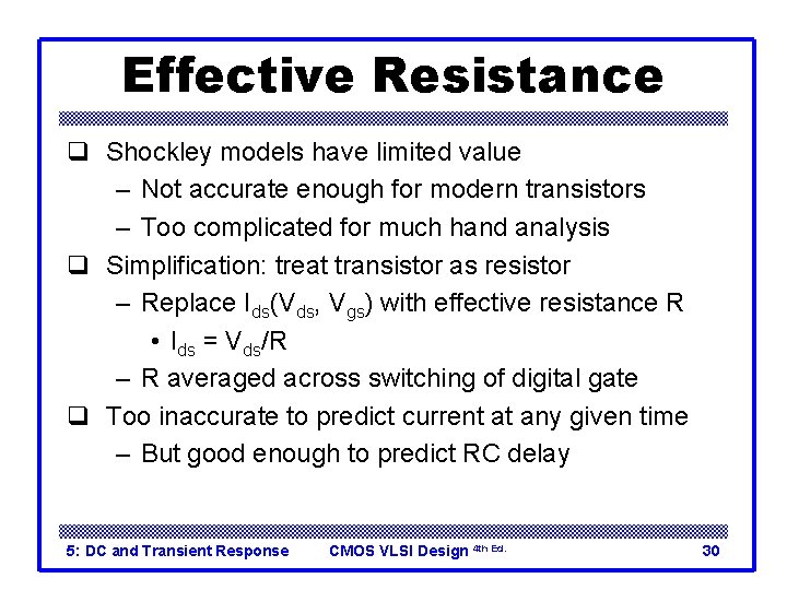
Effective Resistance q Shockley models have limited value – Not accurate enough for modern transistors – Too complicated for much hand analysis q Simplification: treat transistor as resistor – Replace Ids(Vds, Vgs) with effective resistance R • Ids = Vds/R – R averaged across switching of digital gate q Too inaccurate to predict current at any given time – But good enough to predict RC delay 5: DC and Transient Response CMOS VLSI Design 4 th Ed. 30
Delay Estimation Approach 2 CMOS VLSI Design 4 th Ed.
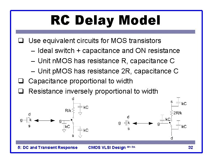
RC Delay Model q Use equivalent circuits for MOS transistors – Ideal switch + capacitance and ON resistance – Unit n. MOS has resistance R, capacitance C – Unit p. MOS has resistance 2 R, capacitance C q Capacitance proportional to width q Resistance inversely proportional to width 5: DC and Transient Response CMOS VLSI Design 4 th Ed. 32
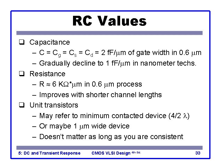
RC Values q Capacitance – C = Cg = Cs = Cd = 2 f. F/mm of gate width in 0. 6 mm – Gradually decline to 1 f. F/mm in nanometer techs. q Resistance – R 6 KW*mm in 0. 6 mm process – Improves with shorter channel lengths q Unit transistors – May refer to minimum contacted device (4/2 l) – Or maybe 1 mm wide device – Doesn’t matter as long as you are consistent 5: DC and Transient Response CMOS VLSI Design 4 th Ed. 33
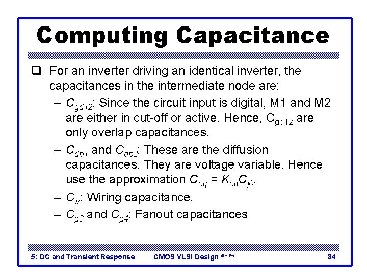
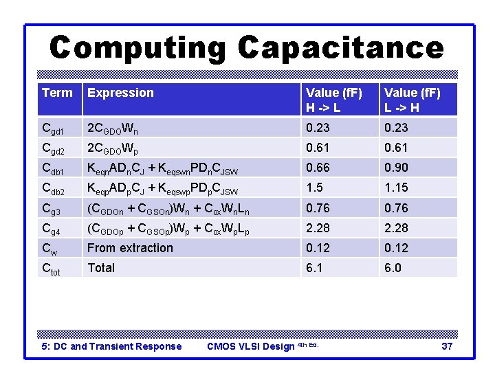
Computing Capacitance q For an inverter driving an identical inverter, the capacitances in the intermediate node are: – Cgd 12: Since the circuit input is digital, M 1 and M 2 are either in cut-off or active. Hence, Cgd 12 are only overlap capacitances. – Cdb 1 and Cdb 2: These are the diffusion capacitances. They are voltage variable. Hence use the approximation Ceq = Keq. Cj 0. – Cw: Wiring capacitance. – Cg 3 and Cg 4: Fanout capacitances 5: DC and Transient Response CMOS VLSI Design 4 th Ed. 34
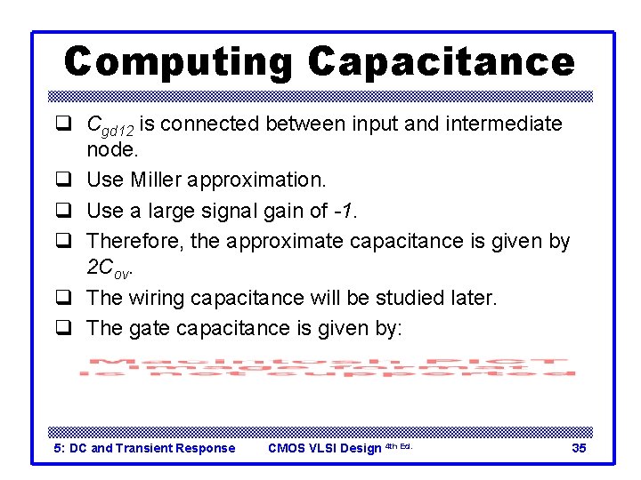
Computing Capacitance q Cgd 12 is connected between input and intermediate node. q Use Miller approximation. q Use a large signal gain of -1. q Therefore, the approximate capacitance is given by 2 Cov. q The wiring capacitance will be studied later. q The gate capacitance is given by: 5: DC and Transient Response CMOS VLSI Design 4 th Ed. 35
Computing Capacitance q Actually, there a few errors in the Cfanout calculation. – Miller effect is ignored here. • Not too bad because Vout of second gate does not change too much while the calculation is being done. – Channel capacitance is assumed to be constant. • It varies between (2/3)WLCox and WLCox. q The total error observed is about 10%. 5: DC and Transient Response CMOS VLSI Design 4 th Ed. 36
Computing Capacitance Term Expression Value (f. F) H -> L Value (f. F) L -> H Cgd 1 2 CGDOWn 0. 23 Cgd 2 2 CGDOWp 0. 61 Cdb 1 Keqn. ADn. CJ + Keqswn. PDn. CJSW 0. 66 0. 90 Cdb 2 Keqp. ADp. CJ + Keqswp. PDp. CJSW 1. 5 1. 15 Cg 3 (CGDOn + CGSOn)Wn + Cox. Wn. Ln 0. 76 Cg 4 (CGDOp + CGSOp)Wp + Cox. Wp. Lp 2. 28 Cw From extraction 0. 12 Ctot Total 6. 1 6. 0 5: DC and Transient Response CMOS VLSI Design 4 th Ed. 37
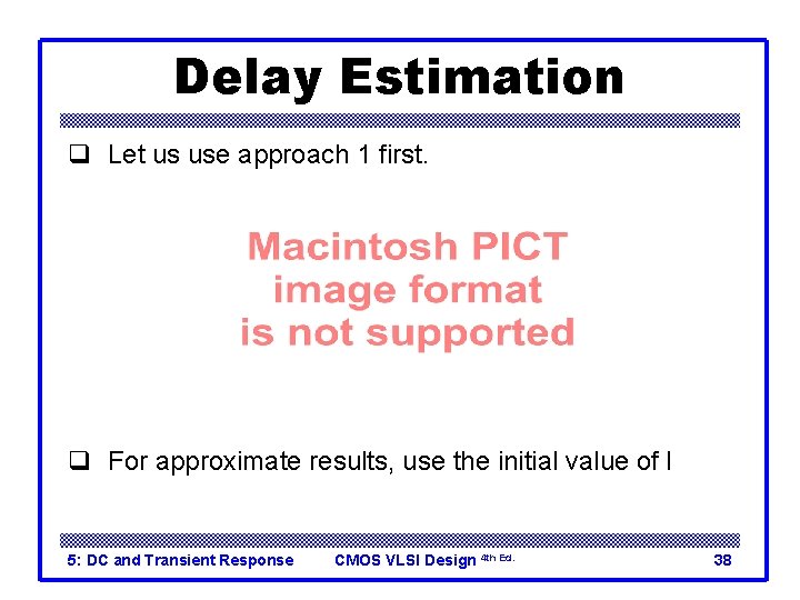
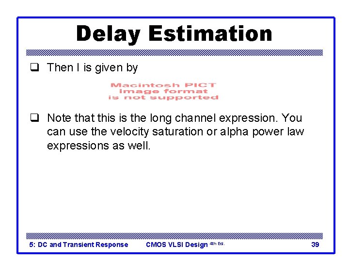
Delay Estimation q Let us use approach 1 first. q For approximate results, use the initial value of I 5: DC and Transient Response CMOS VLSI Design 4 th Ed. 38
Delay Estimation q Then I is given by q Note that this is the long channel expression. You can use the velocity saturation or alpha power law expressions as well. 5: DC and Transient Response CMOS VLSI Design 4 th Ed. 39
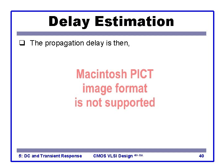
Delay Estimation q The propagation delay is then, 5: DC and Transient Response CMOS VLSI Design 4 th Ed. 40
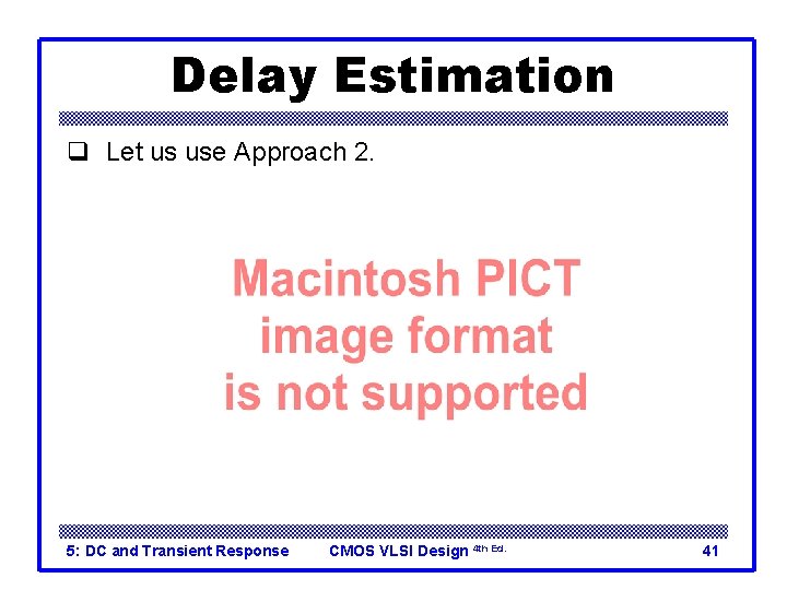
Delay Estimation q Let us use Approach 2. 5: DC and Transient Response CMOS VLSI Design 4 th Ed. 41
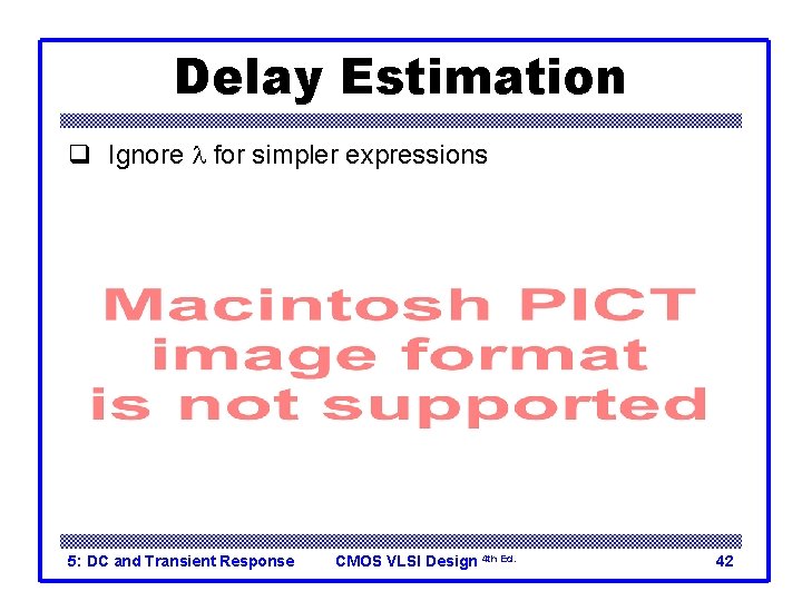
Delay Estimation q Ignore l for simpler expressions 5: DC and Transient Response CMOS VLSI Design 4 th Ed. 42
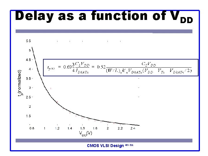
Delay Estimation q Keep C small q Increase transistor sizes – Is there a limit? q Increase supply voltage – Does this really work? 5: DC and Transient Response CMOS VLSI Design 4 th Ed. 43
Delay as a function of VDD CMOS VLSI Design 4 th Ed.
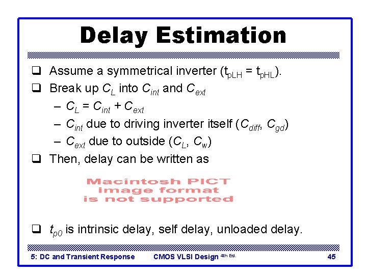
Delay Estimation q Assume a symmetrical inverter (tp. LH = tp. HL). q Break up CL into Cint and Cext – CL = Cint + Cext – Cint due to driving inverter itself (Cdiff, Cgd) – Cext due to outside (CL, Cw) q Then, delay can be written as q tp 0 is intrinsic delay, self delay, unloaded delay. 5: DC and Transient Response CMOS VLSI Design 4 th Ed. 45
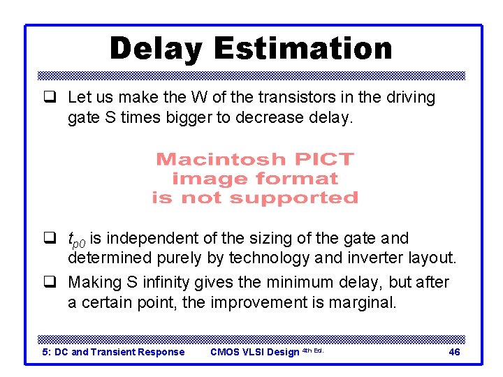
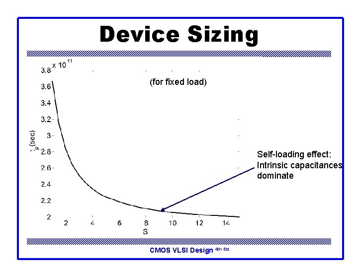
Delay Estimation q Let us make the W of the transistors in the driving gate S times bigger to decrease delay. q tp 0 is independent of the sizing of the gate and determined purely by technology and inverter layout. q Making S infinity gives the minimum delay, but after a certain point, the improvement is marginal. 5: DC and Transient Response CMOS VLSI Design 4 th Ed. 46
Device Sizing (for fixed load) Self-loading effect: Intrinsic capacitances dominate CMOS VLSI Design 4 th Ed.
Device Sizing q So far, we have tried to make tp. HL = tp. LH. q Is this optimum? 5: DC and Transient Response CMOS VLSI Design 4 th Ed. 48
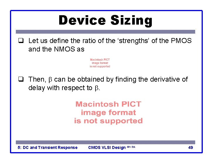
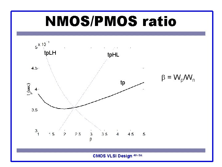
Device Sizing q Let us define the ratio of the ‘strengths’ of the PMOS and the NMOS as q Then, b can be obtained by finding the derivative of delay with respect to b. 5: DC and Transient Response CMOS VLSI Design 4 th Ed. 49
NMOS/PMOS ratio tp. LH tp. HL tp CMOS VLSI Design 4 th Ed. b = Wp/Wn
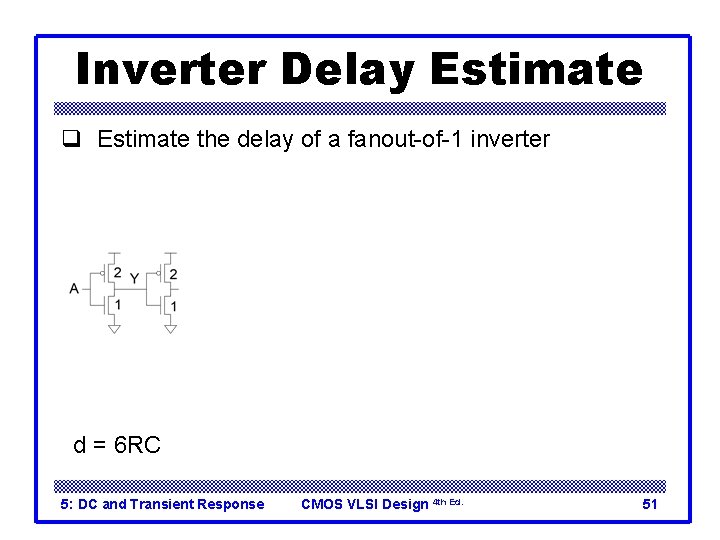
Inverter Delay Estimate q Estimate the delay of a fanout-of-1 inverter d = 6 RC 5: DC and Transient Response CMOS VLSI Design 4 th Ed. 51
Delay Model Comparison 5: DC and Transient Response CMOS VLSI Design 4 th Ed. 52
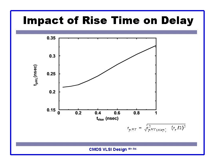
Impact of Rise Time on Delay CMOS VLSI Design 4 th Ed.
Driving Large Loads q Let us take the case of one unit inverter trying to drive a large capacitance, CL. q Let us add one extra inverter as a buffer. q This inverter is u times the unit inverter. q CL is x times larger than the capacitance of the unit inverter. q What is the size of the buffering inverter? q Ignore self loading because the external loads are already large. 5: DC and Transient Response CMOS VLSI Design 4 th Ed. 54
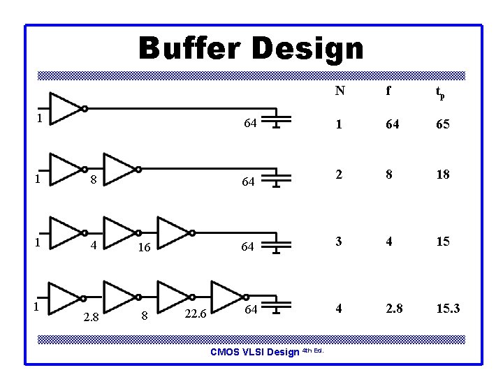
Driving Large Loads q By writing the expressions and taking derivatives, q Take x = 1000. q Unbuffered delay is 1000 tp 0. q Buffered delay is approximately 64 tp 0. 5: DC and Transient Response CMOS VLSI Design 4 th Ed. 55
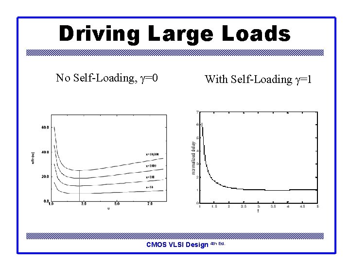
Driving Large Loads q If this is still not good enough, let us use a chain of inverters, each u times larger than the previous one. q For x=1000, tp = 19 tp 0. q However, for small u, self loading cannot be ignored. 5: DC and Transient Response CMOS VLSI Design 4 th Ed. 56
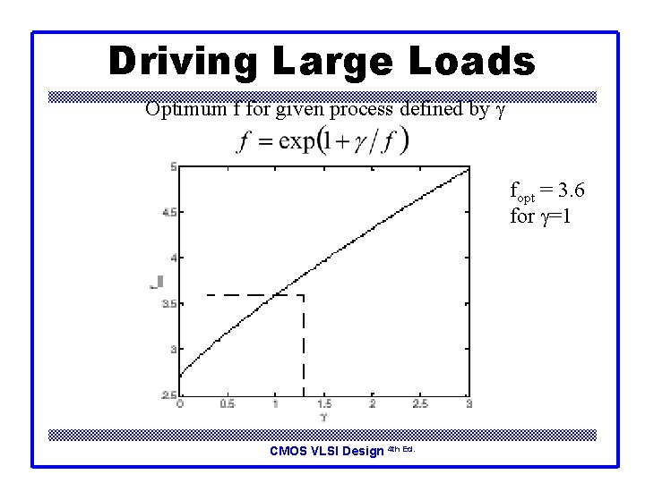
Driving Large Loads q Define a g and an f such that, q Take N-1 partial derivatives. The result is such that all fj should be identical. 5: DC and Transient Response CMOS VLSI Design 4 th Ed. 57
Driving Large Loads q Then, q To find N, 5: DC and Transient Response CMOS VLSI Design 4 th Ed. 58
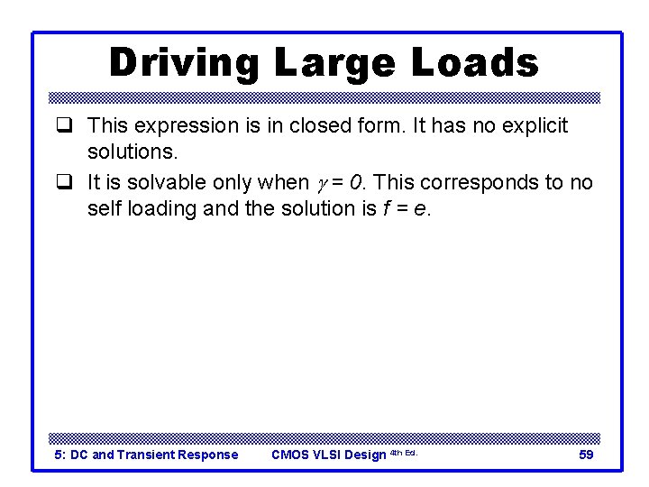
Driving Large Loads q This expression is in closed form. It has no explicit solutions. q It is solvable only when g = 0. This corresponds to no self loading and the solution is f = e. 5: DC and Transient Response CMOS VLSI Design 4 th Ed. 59
Driving Large Loads Optimum f for given process defined by g fopt = 3. 6 for g=1 CMOS VLSI Design 4 th Ed.
Driving Large Loads No Self-Loading, g=0 With Self-Loading g=1 CMOS VLSI Design 4 th Ed.
Buffer Design 1 f tp 1 64 65 2 8 18 64 3 4 15 64 4 2. 8 15. 3 64 1 8 1 4 16 2. 8 8 1 N 64 22. 6 CMOS VLSI Design 4 th Ed.
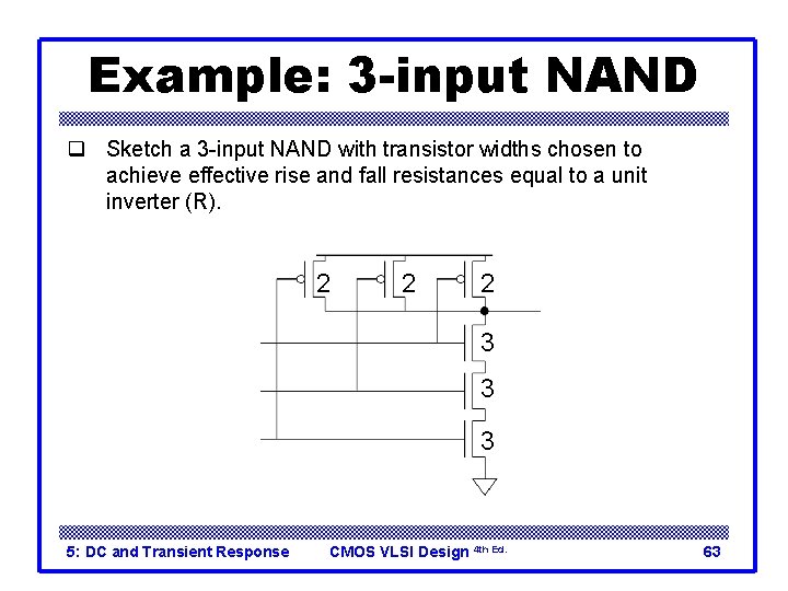
Example: 3 -input NAND q Sketch a 3 -input NAND with transistor widths chosen to achieve effective rise and fall resistances equal to a unit inverter (R). 2 2 2 3 3 3 5: DC and Transient Response CMOS VLSI Design 4 th Ed. 63
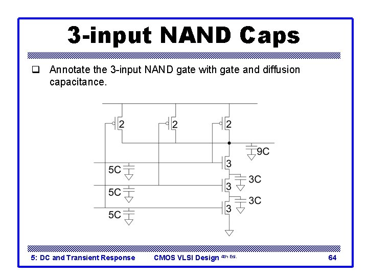
3 -input NAND Caps q Annotate the 3 -input NAND gate with gate and diffusion capacitance. 5: DC and Transient Response CMOS VLSI Design 4 th Ed. 64
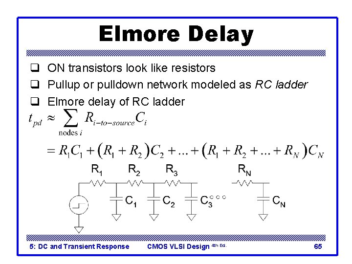
Elmore Delay q ON transistors look like resistors q Pullup or pulldown network modeled as RC ladder q Elmore delay of RC ladder 5: DC and Transient Response CMOS VLSI Design 4 th Ed. 65
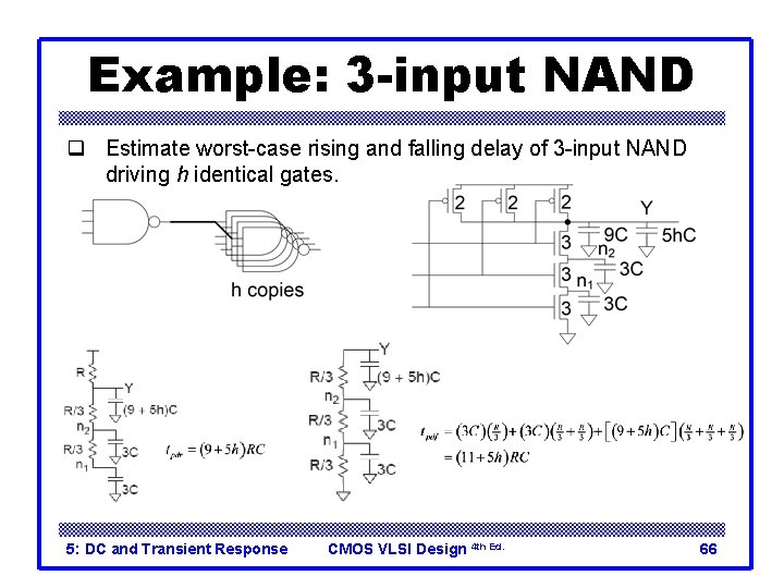
Example: 3 -input NAND q Estimate worst-case rising and falling delay of 3 -input NAND driving h identical gates. 5: DC and Transient Response CMOS VLSI Design 4 th Ed. 66
Delay Components q Delay has two parts – Parasitic delay • 9 or 11 RC • Independent of load – Effort delay • 5 h RC • Proportional to load capacitance 5: DC and Transient Response CMOS VLSI Design 4 th Ed. 67
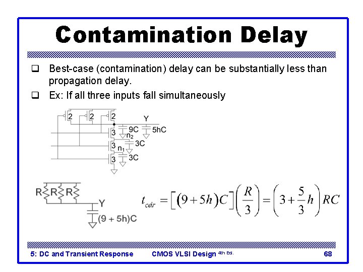
Contamination Delay q Best-case (contamination) delay can be substantially less than propagation delay. q Ex: If all three inputs fall simultaneously 5: DC and Transient Response CMOS VLSI Design 4 th Ed. 68
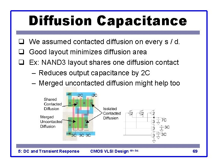
Diffusion Capacitance q We assumed contacted diffusion on every s / d. q Good layout minimizes diffusion area q Ex: NAND 3 layout shares one diffusion contact – Reduces output capacitance by 2 C – Merged uncontacted diffusion might help too 5: DC and Transient Response CMOS VLSI Design 4 th Ed. 69
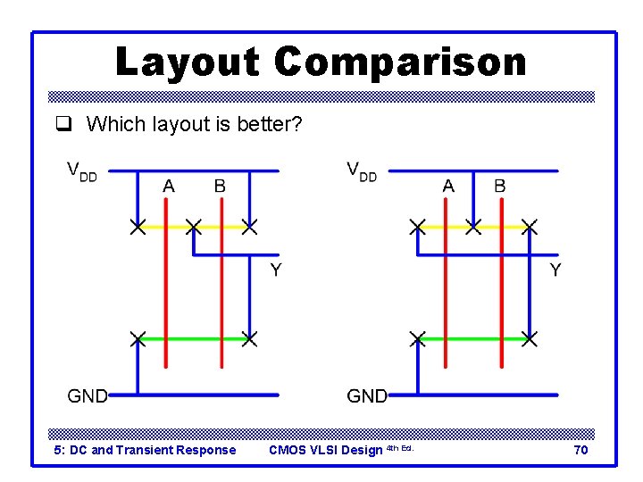
Layout Comparison q Which layout is better? 5: DC and Transient Response CMOS VLSI Design 4 th Ed. 70
Delay Calculations q The above solutions based on Elmore Delay are not accurate. q Capacitors discharge in order. q First, M 1 discharges and it is in active mode q Then, M 2 starts discharging. Assume first node does not change much, 5: DC and Transient Response CMOS VLSI Design 4 th Ed. 71
Delay Calculations q Once all the nodes are discharged, then the Elmore formulation above can be applied. q However, this approach is also not accurate because – Internal nodes discharge in order, but the first node does not remain constant while the second one is discharging, etc. – Elmore formula is an upper bound and not exact. 5: DC and Transient Response CMOS VLSI Design 4 th Ed. 72
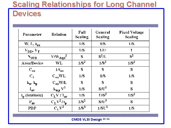
Scaling Relationships for Long Channel Devices CMOS VLSI Design 4 th Ed.
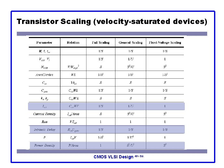
Transistor Scaling (velocity-saturated devices) CMOS VLSI Design 4 th Ed.