Introduzione ai rivelatori fotomoltiplicatori al silicio Nicola Serra



- Slides: 66

Introduzione ai rivelatori fotomoltiplicatori al silicio Nicola Serra, FBK (Trento)

Outline • Introduction to Si. PMs • Si. PMs Low light detection problem Device structure and basic device operation (GM-APD) Fundamental Si. PM parameters • Si. PM technology and characterization at FBK – Technology, design and fabrication – Characterization • Application example December 23, 2021 IV scuola Nazionale Biennale Rivelatori – INFN – LNL 2

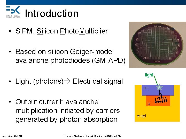
Introduction • Si. PM: Silicon Photo. Multiplier • Based on silicon Geiger-mode avalanche photodiodes (GM-APD) • Light (photons) Electrical signal light n+ • Output current: avalanche multiplication initiated by carriers generated by photon absorption December 23, 2021 IV scuola Nazionale Biennale Rivelatori – INFN – LNL p p epi 3

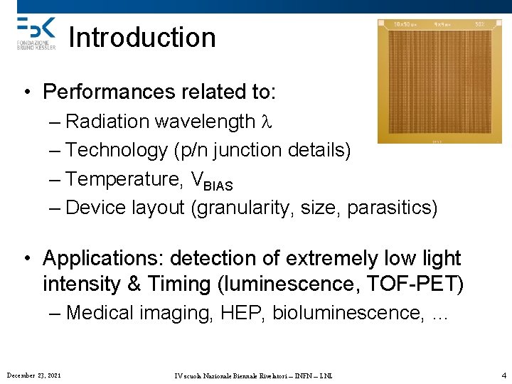
Introduction • Performances related to: – Radiation wavelength l – Technology (p/n junction details) – Temperature, VBIAS – Device layout (granularity, size, parasitics) • Applications: detection of extremely low light intensity & Timing (luminescence, TOF-PET) – Medical imaging, HEP, bioluminescence, … December 23, 2021 IV scuola Nazionale Biennale Rivelatori – INFN – LNL 4

Outline • Introduction to Si. PMs • Si. PMs Low light detection problem Device structure and basic device operation (GM-APD) Fundamental Si. PM parameters • Si. PM technology and characterization at FBK – Technology, design and fabrication – Characterization • Application example December 23, 2021 IV scuola Nazionale Biennale Rivelatori – INFN – LNL 5

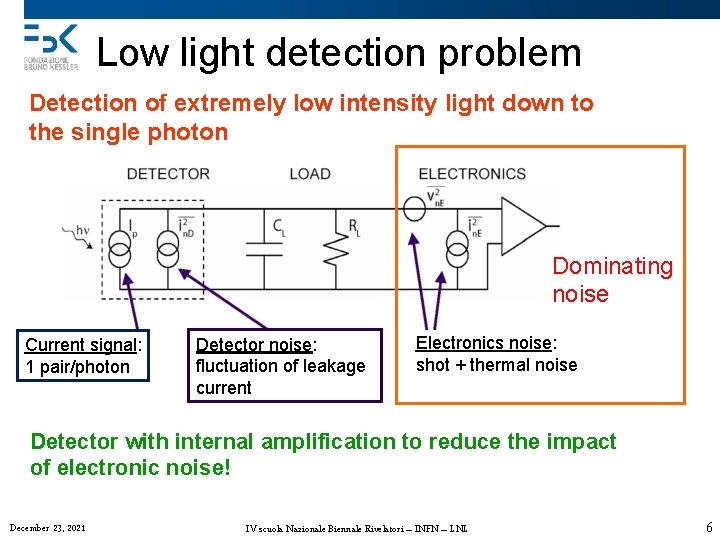
Low light detection problem Detection of extremely low intensity light down to the single photon Dominating noise Current signal: 1 pair/photon Detector noise: fluctuation of leakage current Electronics noise: shot + thermal noise Detector with internal amplification to reduce the impact of electronic noise! December 23, 2021 IV scuola Nazionale Biennale Rivelatori – INFN – LNL 6

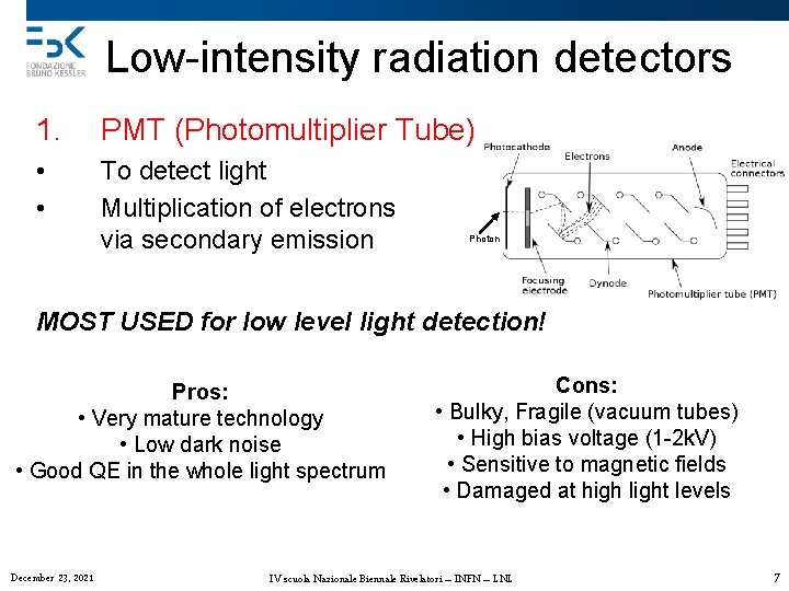
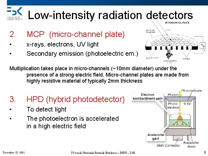
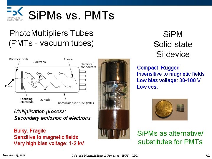
Low-intensity radiation detectors 1. PMT (Photomultiplier Tube) • • To detect light Multiplication of electrons via secondary emission Photon MOST USED for low level light detection! Pros: • Very mature technology • Low dark noise • Good QE in the whole light spectrum December 23, 2021 Cons: • Bulky, Fragile (vacuum tubes) • High bias voltage (1 -2 k. V) • Sensitive to magnetic fields • Damaged at high light levels IV scuola Nazionale Biennale Rivelatori – INFN – LNL 7

Low-intensity radiation detectors 2. MCP (micro-channel plate) • • x-rays, electrons, UV light Secondary emission (photoelectric em. ) Multiplication takes place in micro-channels (~10 mm diameter) under the presence of a strong electric field. Micro-channel plates are made from highly resistive material of typically 2 mm thickness 3. HPD (hybrid photodetector) • • To detect light The photoelectron is accelerated in a high electric field December 23, 2021 IV scuola Nazionale Biennale Rivelatori – INFN – LNL 8

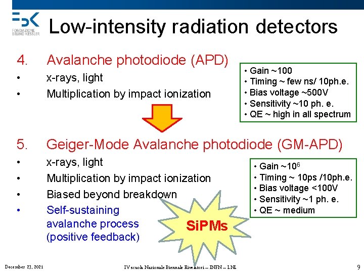
Low-intensity radiation detectors 4. Avalanche photodiode (APD) • • x-rays, light Multiplication by impact ionization 5. Geiger-Mode Avalanche photodiode (GM-APD) • • x-rays, light Multiplication by impact ionization Biased beyond breakdown Self-sustaining avalanche process Si. PMs (positive feedback) December 23, 2021 IV scuola Nazionale Biennale Rivelatori – INFN – LNL • Gain ~100 • Timing ~ few ns/ 10 ph. e. • Bias voltage ~500 V • Sensitivity ~10 ph. e. • QE ~ high in all spectrum • Gain ~106 • Timing ~ 10 ps /10 ph. e. • Bias voltage <100 V • Sensitivity ~1 ph. e. • QE ~ medium 9

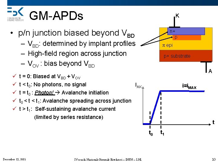
GM-APDs K • p/n junction biased beyond VBD n+ p – VBD: determined by implant profiles – High-field region across junction – VOV : bias beyond VBD ü ü ü p epi p+ substrate A t = 0: Biased at VBD + VOV t < t 0: No photons, no signal t = t 0 : Photon! Avalanche initiation IAK i=i. MAX t 0 < t 1: Avalanche spreading across junction t > t 1: Self-sustaining avalanche current (limited by series resistance) t t 0 December 23, 2021 IV scuola Nazionale Biennale Rivelatori – INFN – LNL t 1 10

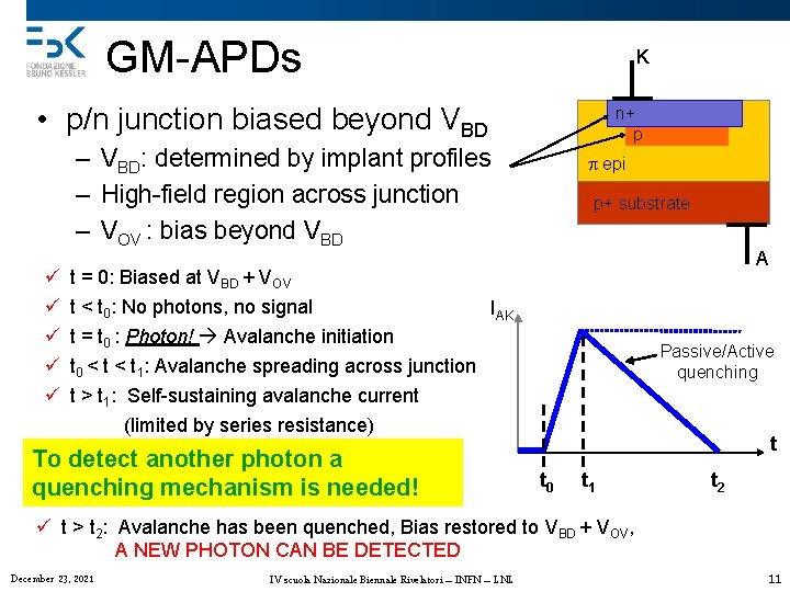
GM-APDs K • p/n junction biased beyond VBD n+ p – VBD: determined by implant profiles – High-field region across junction – VOV : bias beyond VBD ü ü ü p epi p+ substrate A t = 0: Biased at VBD + VOV t < t 0: No photons, no signal t = t 0 : Photon! Avalanche initiation IAK Passive/Active quenching t 0 < t 1: Avalanche spreading across junction t > t 1: Self-sustaining avalanche current (limited by series resistance) To detect another photon a quenching mechanism is needed! t t 0 t 1 t 2 ü t > t 2: Avalanche has been quenched, Bias restored to VBD + VOV, A NEW PHOTON CAN BE DETECTED December 23, 2021 IV scuola Nazionale Biennale Rivelatori – INFN – LNL 11

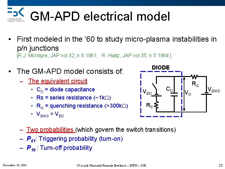
GM-APD electrical model • First modeled in the ’ 60 to study micro-plasma instabilities in p/n junctions [R. J. Mc. Intyre, JAP vol. 32, n. 6 1961; R. Haitz, JAP vol. 35, n. 5 1964 ] DIODE • The GM-APD model consists of: – The equivalent circuit • • CD = diode capacitance Rs = series resistance (~1 k. W) RQ = quenching resistance (>300 k. W) VBIAS > VBD CD RQ VD VBIAS RS – Two probabilities (which govern the switch transitions) – P 01: Triggering probability (turn-on) – P 10 : Turn-off probability December 23, 2021 IV scuola Nazionale Biennale Rivelatori – INFN – LNL 12

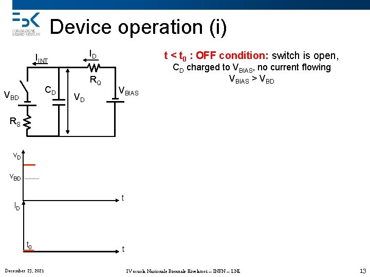
Device operation (i) ID IINT CD VBD RQ VD t < t 0 : OFF condition: switch is open, VBIAS CD charged to VBIAS, no current flowing VBIAS > VBD RS v. D v. BD t ID t 0 December 23, 2021 t IV scuola Nazionale Biennale Rivelatori – INFN – LNL 13

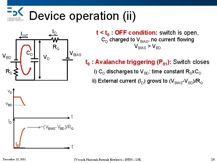
Device operation (ii) ID IINT CD VBD RQ VD t < t 0 : OFF condition: switch is open, VBIAS CD charged to VBIAS, no current flowing VBIAS > VBD t 0 : Avalanche triggering (P 01): Switch closes RS i) CD discharges to VBD: time constant RSx. CD ii) External current (ID) grows to (VBIAS-VBD)/RQ v. D v. BD t ID ~(VBIAS-VBD)/RQ t 0 t 1 December 23, 2021 t 2 t IV scuola Nazionale Biennale Rivelatori – INFN – LNL 14

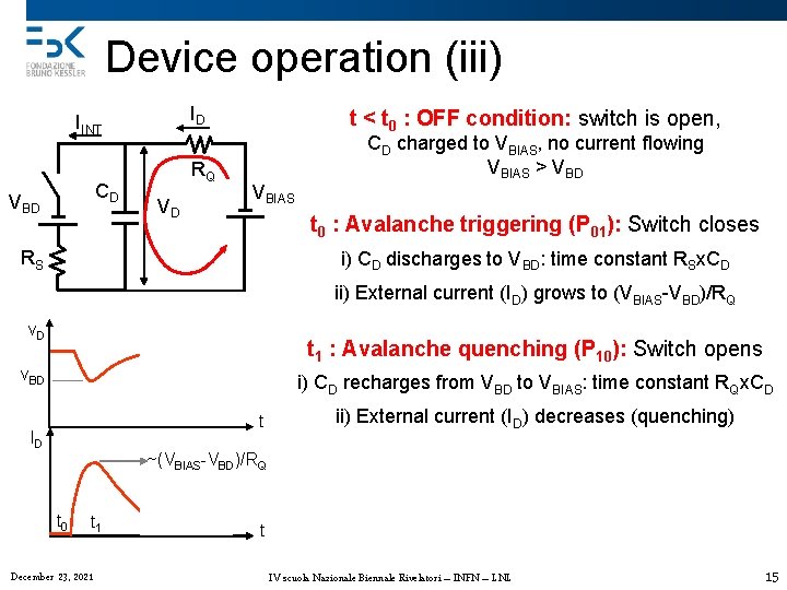
Device operation (iii) ID IINT CD VBD RQ VD t < t 0 : OFF condition: switch is open, VBIAS CD charged to VBIAS, no current flowing VBIAS > VBD t 0 : Avalanche triggering (P 01): Switch closes RS i) CD discharges to VBD: time constant RSx. CD ii) External current (ID) grows to (VBIAS-VBD)/RQ v. D t 1 : Avalanche quenching (P 10): Switch opens v. BD i) CD recharges from VBD to VBIAS: time constant RQx. CD t ID ii) External current (ID) decreases (quenching) ~(VBIAS-VBD)/RQ t 0 t 1 December 23, 2021 t 2 t IV scuola Nazionale Biennale Rivelatori – INFN – LNL 15

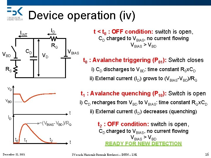
Device operation (iv) ID IINT CD VBD RQ VD t < t 0 : OFF condition: switch is open, VBIAS CD charged to VBIAS, no current flowing VBIAS > VBD t 0 : Avalanche triggering (P 01): Switch closes RS i) CD discharges to VBD: time constant RSx. CD ii) External current (ID) grows to (VBIAS-VBD)/RQ v. D t 1 : Avalanche quenching (P 10): Switch is open v. BD i) CD recharges from VBD to VBIAS: time constant RQx. CD t ID ~(VBIAS-VBD)/RQ t 0 t 1 December 23, 2021 t 2 t ii) External current (ID) decreases (quenching) t 2 : OFF condition: switch is open, CD charged to VBIAS, no current flowing VBIAS > VBD READY FOR NEW DETECTION IV scuola Nazionale Biennale Rivelatori – INFN – LNL 16

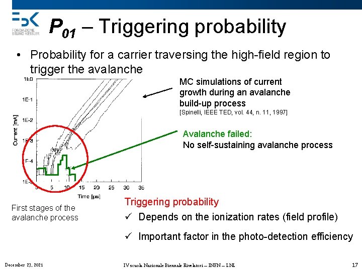
P 01 – Triggering probability • Probability for a carrier traversing the high-field region to trigger the avalanche MC simulations of current growth during an avalanche build-up process [Spinelli, IEEE TED, vol. 44, n. 11, 1997] Avalanche failed: No self-sustaining avalanche process First stages of the avalanche process Triggering probability ü Depends on the ionization rates (field profile) ü Important factor in the photo-detection efficiency December 23, 2021 IV scuola Nazionale Biennale Rivelatori – INFN – LNL 17

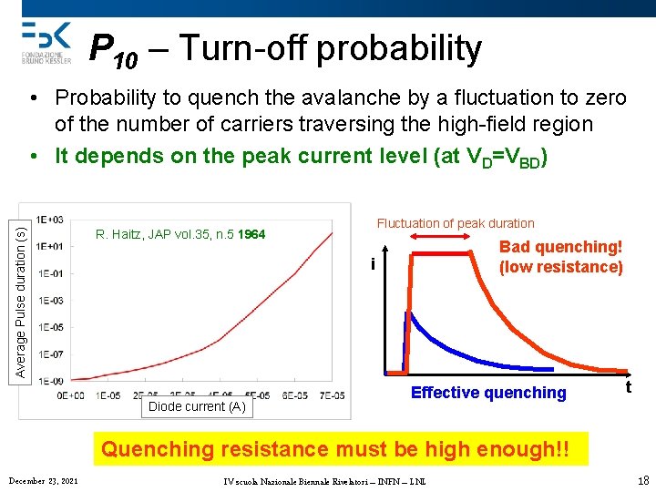
P 10 – Turn-off probability Average Pulse duration (s) • Probability to quench the avalanche by a fluctuation to zero of the number of carriers traversing the high-field region • It depends on the peak current level (at VD=VBD) Fluctuation of peak duration R. Haitz, JAP vol. 35, n. 5 1964 Bad quenching! (low resistance) i Diode current (A) Effective quenching t Quenching resistance must be high enough!! December 23, 2021 IV scuola Nazionale Biennale Rivelatori – INFN – LNL 18

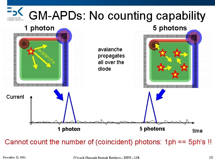
GM-APDs: No counting capability 1 photon av al an 5 photons avalanche propagates all over the diode ch e Current 1 photon 5 photons time Cannot count the number of (coincident) photons: 1 ph == 5 ph’s !! December 23, 2021 IV scuola Nazionale Biennale Rivelatori – INFN – LNL 19

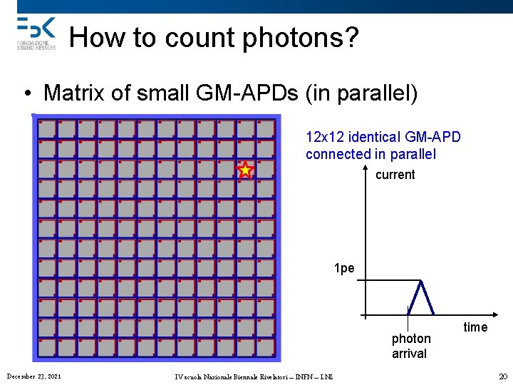
How to count photons? • Matrix of small GM-APDs (in parallel) 12 x 12 identical GM-APD connected in parallel current 1 pe photon arrival December 23, 2021 IV scuola Nazionale Biennale Rivelatori – INFN – LNL time 20

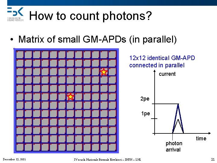
How to count photons? • Matrix of small GM-APDs (in parallel) 12 x 12 identical GM-APD connected in parallel current 2 pe 1 pe photon arrival December 23, 2021 IV scuola Nazionale Biennale Rivelatori – INFN – LNL time 21

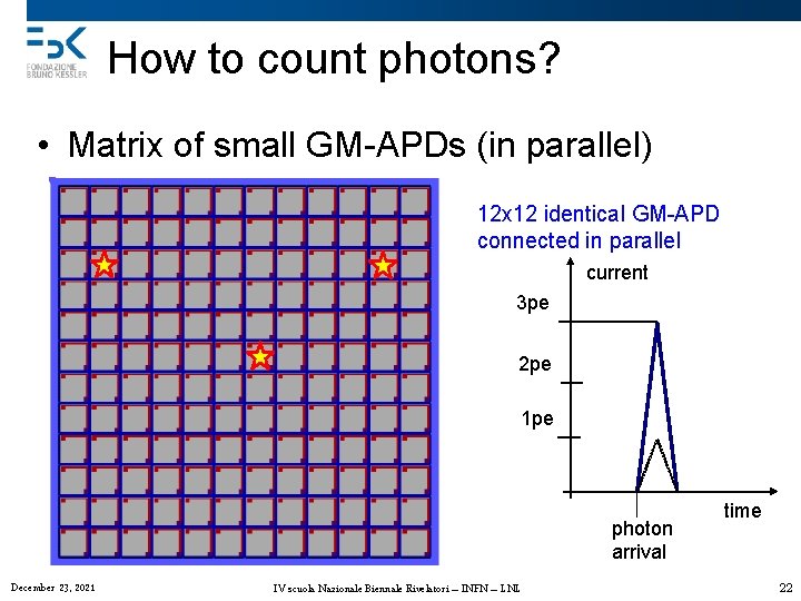
How to count photons? • Matrix of small GM-APDs (in parallel) 12 x 12 identical GM-APD connected in parallel current 3 pe 2 pe 1 pe photon arrival December 23, 2021 IV scuola Nazionale Biennale Rivelatori – INFN – LNL time 22

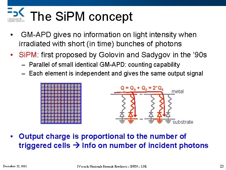
The Si. PM concept • GM-APD gives no information on light intensity when irradiated with short (in time) bunches of photons • Si. PM: first proposed by Golovin and Sadygov in the ’ 90 s – Parallel of small identical GM-APD: counting capability – Each element is independent and gives the same output signal Q = Q 1 + Q 2 = 2*Q 1 metal substrate • Output charge is proportional to the number of triggered cells Info on number of incident photons December 23, 2021 IV scuola Nazionale Biennale Rivelatori – INFN – LNL 23

Outline • Introduction to Si. PMs • Si. PMs Low light detection problem Device structure and basic device operation (GM-APD) Fundamental Si. PM parameters • Si. PM technology and characterization at FBK – Technology, design and fabrication – Characterization • Application example December 23, 2021 IV scuola Nazionale Biennale Rivelatori – INFN – LNL 24

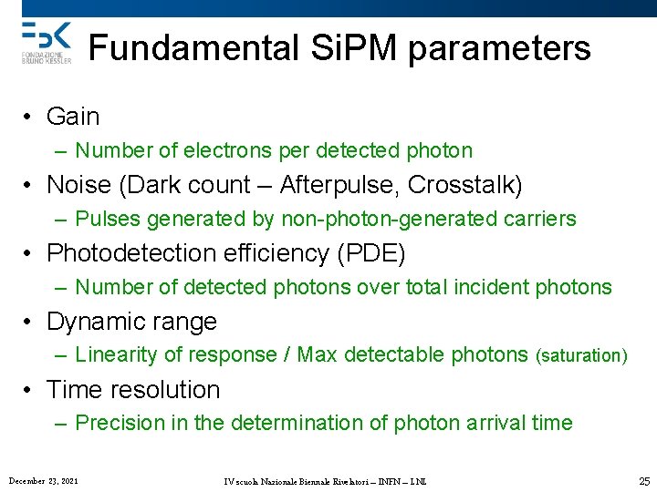
Fundamental Si. PM parameters • Gain – Number of electrons per detected photon • Noise (Dark count – Afterpulse, Crosstalk) – Pulses generated by non-photon-generated carriers • Photodetection efficiency (PDE) – Number of detected photons over total incident photons • Dynamic range – Linearity of response / Max detectable photons (saturation) • Time resolution – Precision in the determination of photon arrival time December 23, 2021 IV scuola Nazionale Biennale Rivelatori – INFN – LNL 25

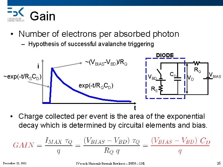
Gain • Number of electrons per absorbed photon – Hypothesis of successful avalanche triggering i DIODE ~(VBIAS-VBD)/RQ ~exp(-t/RSCD) VBD exp(-t/RQCD) CD RQ VD VBIAS RS t • Charge collected per event is the area of the exponential decay which is determined by circuital elements and bias. December 23, 2021 IV scuola Nazionale Biennale Rivelatori – INFN – LNL 26

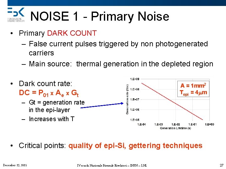
NOISE 1 - Primary Noise • Primary DARK COUNT – False current pulses triggered by non photogenerated carriers – Main source: thermal generation in the depleted region • Dark count rate: DC = P 01 x Ae x Gt A = 1 mm 2 Tepi = 4 mm – Gt = generation rate in the epi-layer – Increases with T • Critical points: quality of epi-Si, gettering techniques December 23, 2021 IV scuola Nazionale Biennale Rivelatori – INFN – LNL 27

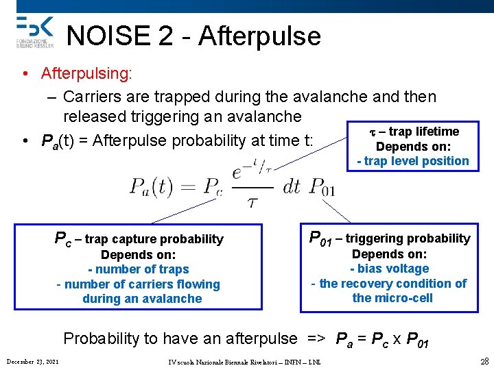
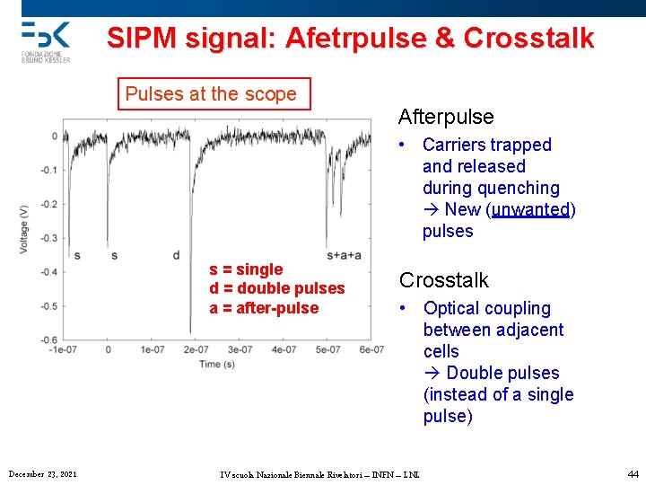
NOISE 2 - Afterpulse • Afterpulsing: – Carriers are trapped during the avalanche and then released triggering an avalanche t – trap lifetime • Pa(t) = Afterpulse probability at time t: Depends on: - trap level position Pc – trap capture probability Depends on: - number of traps - number of carriers flowing during an avalanche P 01 – triggering probability Depends on: - bias voltage - the recovery condition of the micro-cell Probability to have an afterpulse => Pa = Pc x P 01 December 23, 2021 IV scuola Nazionale Biennale Rivelatori – INFN – LNL 28

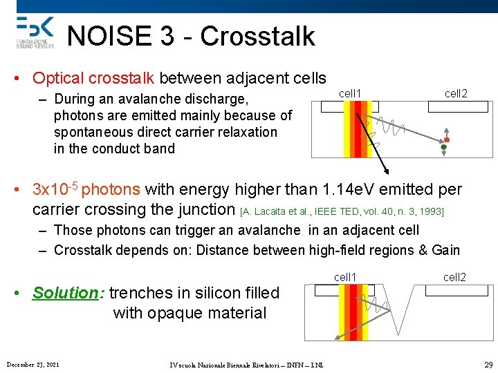
NOISE 3 - Crosstalk • Optical crosstalk between adjacent cells – During an avalanche discharge, photons are emitted mainly because of spontaneous direct carrier relaxation in the conduct band cell 1 cell 2 • 3 x 10 -5 photons with energy higher than 1. 14 e. V emitted per carrier crossing the junction [A. Lacaita et al. , IEEE TED, vol. 40, n. 3, 1993] – Those photons can trigger an avalanche in an adjacent cell – Crosstalk depends on: Distance between high-field regions & Gain • Solution: trenches in silicon filled with opaque material December 23, 2021 IV scuola Nazionale Biennale Rivelatori – INFN – LNL cell 1 cell 2 29

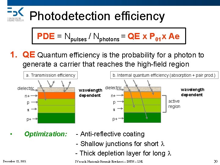
Photodetection efficiency PDE = Npulses / Nphotons = QE x P 01 x Ae 1. QE Quantum efficiency is the probability for a photon to generate a carrier that reaches the high-field region b. Internal quantum efficiency (absorption + pair prod. ) a. Transmission efficiency dielectric n+ • dielectric wavelength dependent n+ p p p+ p+ Optimization: December 23, 2021 wavelength dependent active region - Anti-reflective coating - Shallow junctions for short l - Thick depletion layer for long l IV scuola Nazionale Biennale Rivelatori – INFN – LNL 30

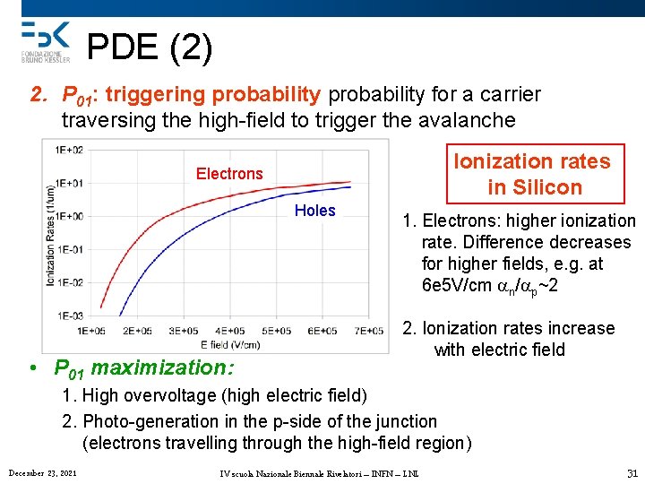
PDE (2) 2. P 01: triggering probability for a carrier traversing the high-field to trigger the avalanche Ionization rates in Silicon Electrons Holes • P 01 maximization: 1. Electrons: higher ionization rate. Difference decreases for higher fields, e. g. at 6 e 5 V/cm an/ap~2 2. Ionization rates increase with electric field 1. High overvoltage (high electric field) 2. Photo-generation in the p-side of the junction (electrons travelling through the high-field region) December 23, 2021 IV scuola Nazionale Biennale Rivelatori – INFN – LNL 31

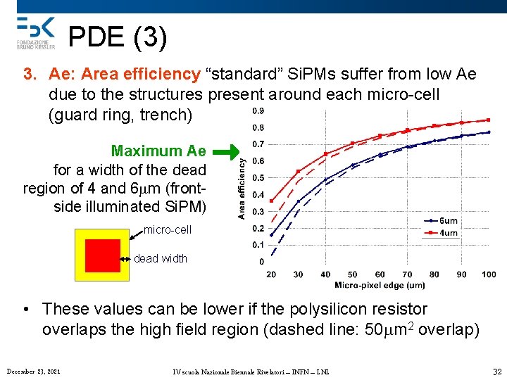
PDE (3) 3. Ae: Area efficiency “standard” Si. PMs suffer from low Ae due to the structures present around each micro-cell (guard ring, trench) Maximum Ae for a width of the dead region of 4 and 6 mm (frontside illuminated Si. PM) micro-cell dead width • These values can be lower if the polysilicon resistor overlaps the high field region (dashed line: 50 mm 2 overlap) December 23, 2021 IV scuola Nazionale Biennale Rivelatori – INFN – LNL 32

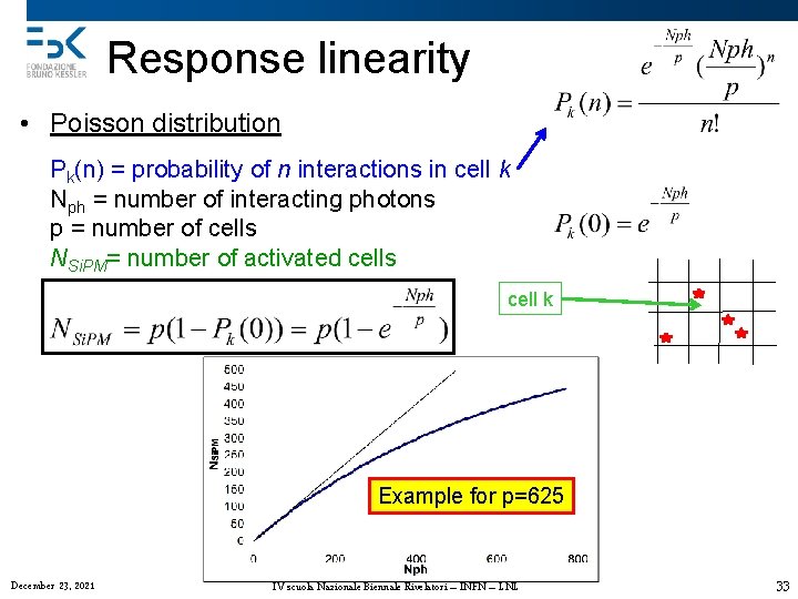
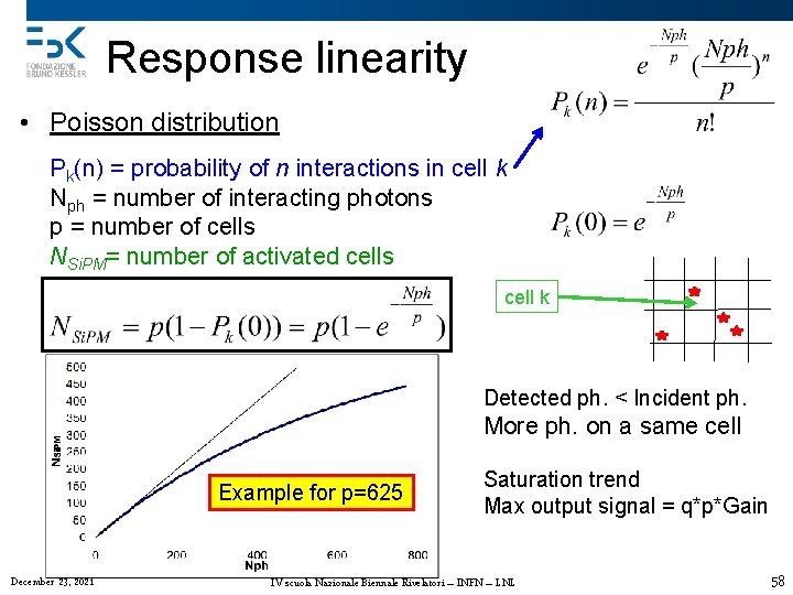
Response linearity • Poisson distribution Pk(n) = probability of n interactions in cell k Nph = number of interacting photons p = number of cells NSi. PM= number of activated cells cell k Example for p=625 December 23, 2021 IV scuola Nazionale Biennale Rivelatori – INFN – LNL 33

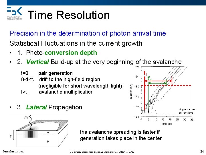
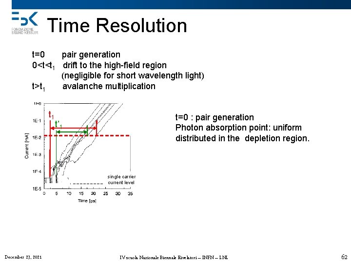
Time Resolution Precision in the determination of photon arrival time Statistical Fluctuations in the current growth: • 1. Photo-conversion depth • 2. Vertical Build-up at the very beginning of the avalanche t=0 pair generation 0<t<t 1 drift to the high-field region (negligible for short wavelength light) t>t 1 avalanche multiplication t 1 t’ 1 • 3. Lateral Propagation single carrier current level the avalanche spreading is faster if generation takes place in the center December 23, 2021 IV scuola Nazionale Biennale Rivelatori – INFN – LNL 34

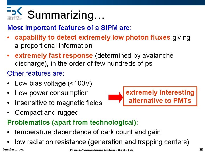
Summarizing… Most important features of a Si. PM are: • capability to detect extremely low photon fluxes giving a proportional information • extremely fast response (determined by avalanche discharge), in the order of few hundreds of ps Other features are: • Low bias voltage (<100 V) extremely interesting • Low power consumption alternative to PMTs • Insensitive to magnetic fields • Compact and rugged Problematics (apart from technological): • temperature dependence of dark count and gain • low radiation resistance (generation and trapping centers) December 23, 2021 IV scuola Nazionale Biennale Rivelatori – INFN – LNL 35

Outline • Introduction to Si. PMs • Si. PMs Low light detection problem Device structure and basic device operation (GM-APD) Fundamental Si. PM parameters • Si. PM technology and characterization at FBK – Technology, design and fabrication – Characterization • Application example December 23, 2021 IV scuola Nazionale Biennale Rivelatori – INFN – LNL 36

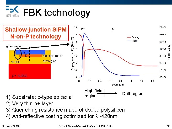
FBK technology Shallow-junction Si. PM N-on-P technology p n+ guard region n+ p p epi high-field region drift region p+ subst. High field region Drift region 1) Substrate: p-type epitaxial 2) Very thin n+ layer 3) Quenching resistance made of doped polysilicon 4) Anti-reflective coating optimized for l~420 nm December 23, 2021 IV scuola Nazionale Biennale Rivelatori – INFN – LNL 37

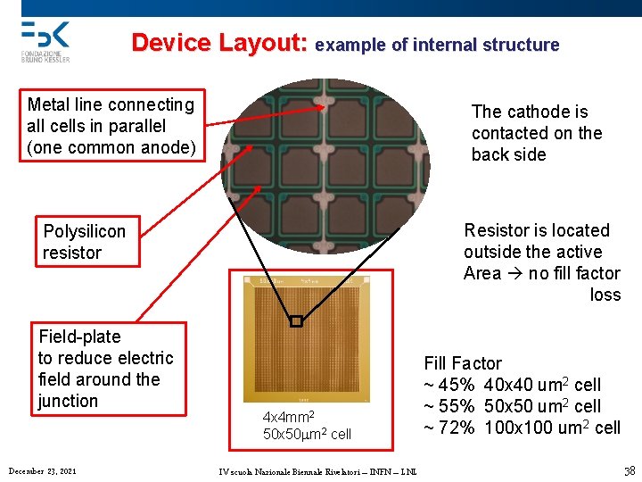
Device Layout: example of internal structure Metal line connecting all cells in parallel (one common anode) The cathode is contacted on the back side Resistor is located outside the active Area no fill factor loss Polysilicon resistor Field-plate to reduce electric field around the junction December 23, 2021 4 x 4 mm 2 50 x 50 mm 2 cell IV scuola Nazionale Biennale Rivelatori – INFN – LNL Fill Factor ~ 45% 40 x 40 um 2 cell ~ 55% 50 x 50 um 2 cell ~ 72% 100 x 100 um 2 cell 38

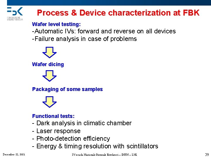
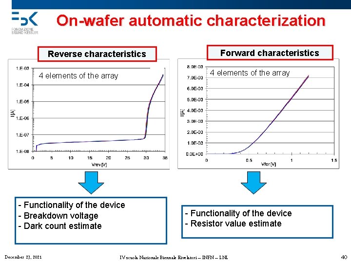
Process & Device characterization at FBK Wafer level testing: -Automatic IVs: forward and reverse on all devices -Failure analysis in case of problems Wafer dicing Packaging of some samples Functional tests: - Dark analysis in climatic chamber - Laser response - Photo-detection efficiency - Energy & timing resolution with scintillators December 23, 2021 IV scuola Nazionale Biennale Rivelatori – INFN – LNL 39

On-wafer automatic characterization Reverse characteristics 4 elements of the array - Functionality of the device - Breakdown voltage - Dark count estimate December 23, 2021 Forward characteristics - Functionality of the device - Resistor value estimate IV scuola Nazionale Biennale Rivelatori – INFN – LNL 40

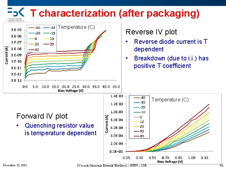
T characterization (after packaging) Temperature (C) Reverse IV plot • Reverse diode current is T dependent • Breakdown (due to i. i. ) has positive T coefficient Temperature (C) Forward IV plot • Quenching resistor value is temperature dependent December 23, 2021 IV scuola Nazionale Biennale Rivelatori – INFN – LNL 41

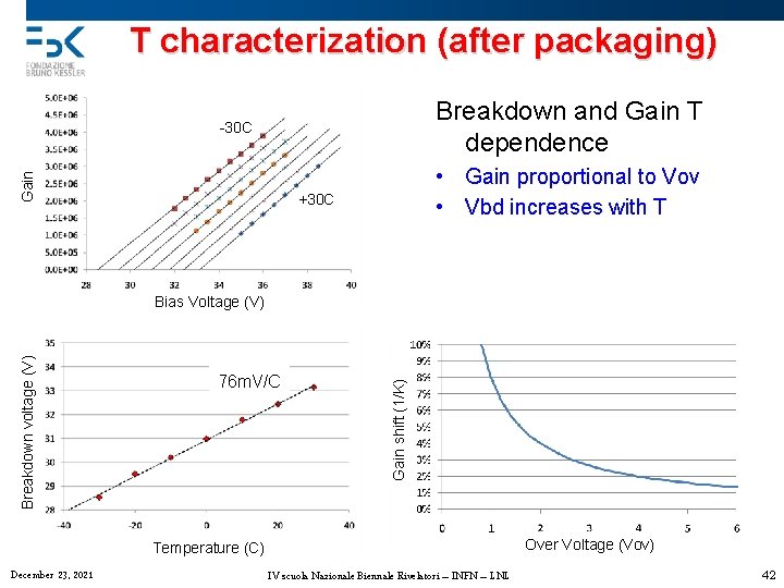
T characterization (after packaging) Breakdown and Gain T dependence Gain -30 C • Gain proportional to Vov • Vbd increases with T +30 C 76 m. V/C Gain shift (1/K) Breakdown voltage (V) Bias Voltage (V) Over Voltage (Vov) Temperature (C) December 23, 2021 IV scuola Nazionale Biennale Rivelatori – INFN – LNL 42

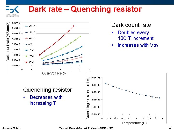
Dark rate – Quenching resistor Dark count rate (HZ/mm 2) Dark count rate • Doubles every 10 C T increment • Increases with Vov Quenching resistor • Decreases with increasing T Quenching resistance (ohm) Over-Voltage (V) Temperature (C) December 23, 2021 IV scuola Nazionale Biennale Rivelatori – INFN – LNL 43

SIPM signal: Afetrpulse & Crosstalk Pulses at the scope Afterpulse • Carriers trapped and released during quenching New (unwanted) pulses s = single d = double pulses a = after-pulse December 23, 2021 Crosstalk • Optical coupling between adjacent cells Double pulses (instead of a single pulse) IV scuola Nazionale Biennale Rivelatori – INFN – LNL 44

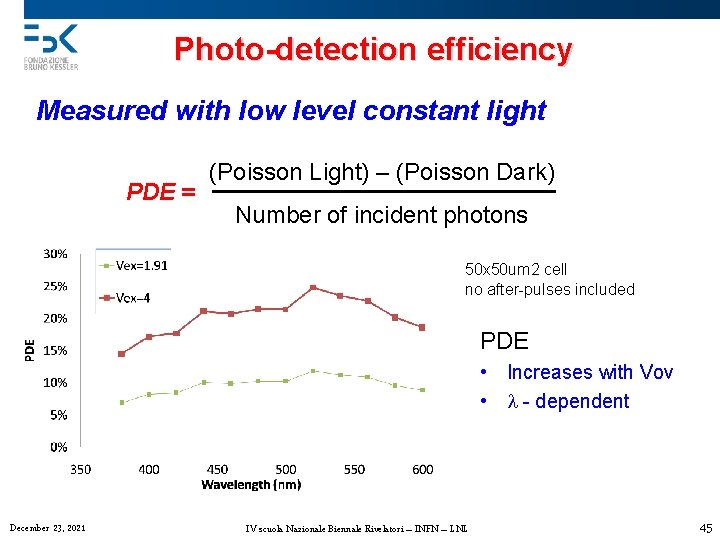
Photo-detection efficiency Measured with low level constant light PDE = (Poisson Light) – (Poisson Dark) Number of incident photons 50 x 50 um 2 cell no after-pulses included PDE • Increases with Vov • l - dependent December 23, 2021 IV scuola Nazionale Biennale Rivelatori – INFN – LNL 45

Outline • Introduction to Si. PMs • Si. PMs Low light detection problem Device structure and basic device operation (GM-APD) Fundamental Si. PM parameters • Si. PM technology and characterization at FBK – Technology, design and fabrication – Characterization • Application example: Time of flight PET December 23, 2021 IV scuola Nazionale Biennale Rivelatori – INFN – LNL 46

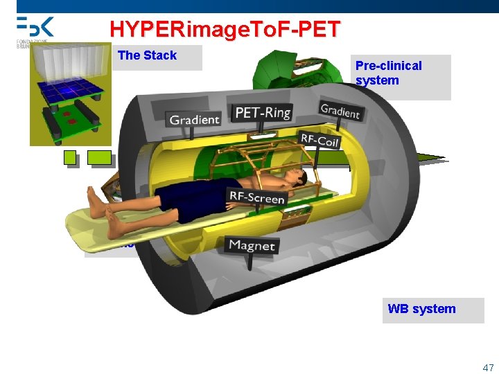
HYPERimage. To. F-PET The Stack Pre-clinical system The module WB system 47

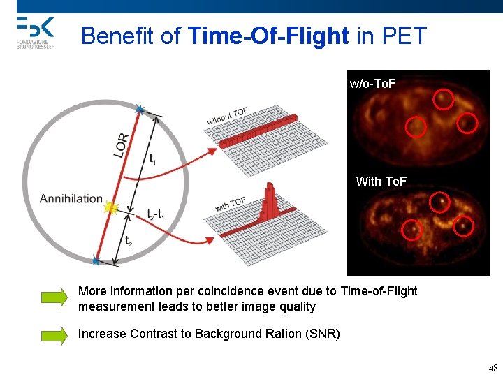
Benefit of Time-Of-Flight in PET w/o-To. F With To. F More information per coincidence event due to Time-of-Flight measurement leads to better image quality Increase Contrast to Background Ration (SNR) 48

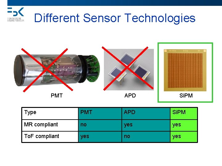
Different Sensor Technologies PMT APD Si. PM Type PMT APD Si. PM MR compliant no yes To. F compliant yes no yes

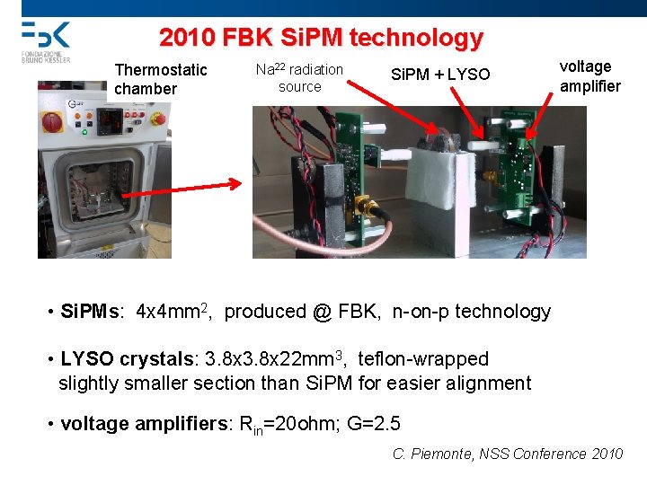
2010 FBK Si. PM technology Thermostatic chamber Na 22 radiation source Si. PM + LYSO voltage amplifier • Si. PMs: 4 x 4 mm 2, produced @ FBK, n-on-p technology • LYSO crystals: 3. 8 x 22 mm 3, teflon-wrapped slightly smaller section than Si. PM for easier alignment • voltage amplifiers: Rin=20 ohm; G=2. 5 C. Piemonte, NSS Conference 2010

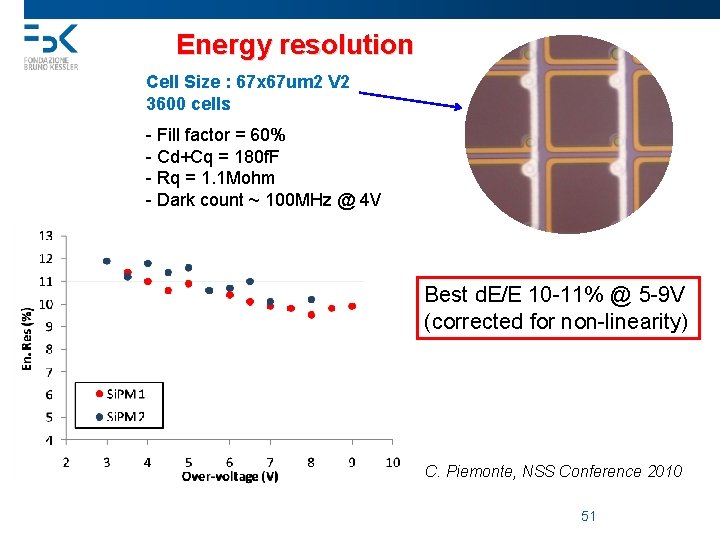
Energy resolution Cell Size : 67 x 67 um 2 V 2 3600 cells - Fill factor = 60% - Cd+Cq = 180 f. F - Rq = 1. 1 Mohm - Dark count ~ 100 MHz @ 4 V Best d. E/E 10 -11% @ 5 -9 V (corrected for non-linearity) C. Piemonte, NSS Conference 2010 51

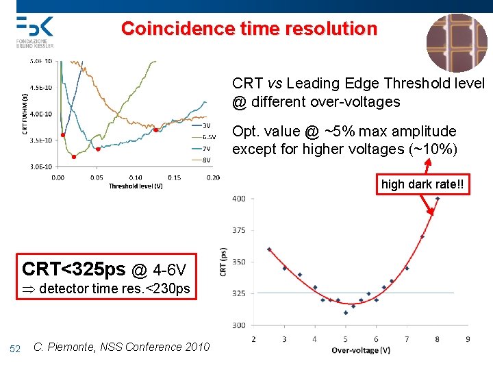
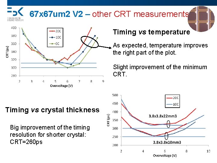
Coincidence time resolution CRT vs Leading Edge Threshold level @ different over-voltages Opt. value @ ~5% max amplitude except for higher voltages (~10%) high dark rate!! CRT<325 ps @ 4 -6 V Þ detector time res. <230 ps 52 C. Piemonte, NSS Conference 2010

Conclusions • Si. PMs: solid-state radiation detectors with competitive performances – – Single photon detection High gain, fast response (TOF capabilities) Not sensitive to magnetic fields Visible light, X-ray, g-ray (medical, HEP, HL security, …) • Si. PM technology is improving quickly – Meeting requirements of the most challenging applications – FBK: state-of-the-art Si. PM devices, consolidated technology • Si. PM performances improvement – PDE, time resolution, Noise – FBK: on-going research activity, major advancements foreseen! December 23, 2021 IV scuola Nazionale Biennale Rivelatori – INFN – LNL 53

Acknowledgments • FBK SRS Group – Claudio Piemonte – – – – Gabriele Giacomini Alberto Gola Elisabetta Mazzuca Alessandro Piazza Tiziana Pro Nicola Serra Alessandro Tarolli Nicola Zorzi December 23, 2021 • Da. Si. PM & MEMS projects IV scuola Nazionale Biennale Rivelatori – INFN – LNL • Hyper-Image project In particular: Philips Research Aachen University of Heidelberg 54

Acknowledgments • FBK SRS Group – Claudio Piemonte – – – – Gabriele Giacomini Alberto Gola Elisabetta Mazzuca Alessandro Piazza Tiziana Pro Nicola Serra Alessandro Tarolli Nicola Zorzi December 23, 2021 • Da. Si. PM & MEMS projects IV scuola Nazionale Biennale Rivelatori – INFN – LNL • Hyper-Image project In particular: Philips Research Aachen University of Heidelberg 55


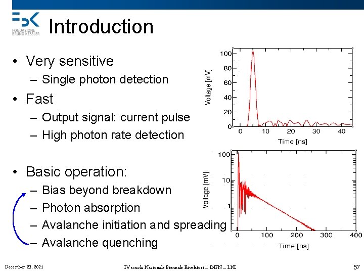
Introduction • Very sensitive – Single photon detection • Fast – Output signal: current pulse – High photon rate detection • Basic operation: – – Bias beyond breakdown Photon absorption Avalanche initiation and spreading Avalanche quenching December 23, 2021 IV scuola Nazionale Biennale Rivelatori – INFN – LNL 57

Response linearity • Poisson distribution Pk(n) = probability of n interactions in cell k Nph = number of interacting photons p = number of cells NSi. PM= number of activated cells cell k Detected ph. < Incident ph. More ph. on a same cell Example for p=625 December 23, 2021 Saturation trend Max output signal = q*p*Gain IV scuola Nazionale Biennale Rivelatori – INFN – LNL 58

Characterization at FBK • Reverse IV measurement: fast test to verify functionality and uniformity of the properties. • Dynamic characterization in dark: for a complete characterization of the output signal and noise properties – Signal shape – Single photon resolution capability – Gain – Noise rate – Temperature dependence • Dynamic characterization in ligth: led/laser source • Photodetection efficiency December 23, 2021 IV scuola Nazionale Biennale Rivelatori – INFN – LNL 59

67 x 67 um 2 V 2 – other CRT measurements Timing vs temperature As expected, temperature improves the right part of the plot. Slight improvement of the minimum CRT. Timing vs crystal thickness Big improvement of the timing resolution for shorter crystal: CRT=260 ps 60

Si. PMs vs. PMTs Photo. Multipliers Tubes (PMTs - vacuum tubes) Si. PM Solid-state Si device Compact, Rugged Insensitive to magnetic fields Low bias voltage: 30 -100 V Low cost Photon Multiplication process: Secondary emission of electrons Bulky, Fragile Sensitive to magnetic fields Very high bias voltage: 1 -2 k. V December 23, 2021 Si. PMs as alternative/ substitutes for PMTs IV scuola Nazionale Biennale Rivelatori – INFN – LNL 61

Time Resolution t=0 pair generation 0<t<t 1 drift to the high-field region (negligible for short wavelength light) t>t 1 avalanche multiplication t 1 t=0 : pair generation Photon absorption point: uniform distributed in the depletion region. t’ 1 single carrier current level December 23, 2021 IV scuola Nazionale Biennale Rivelatori – INFN – LNL 62

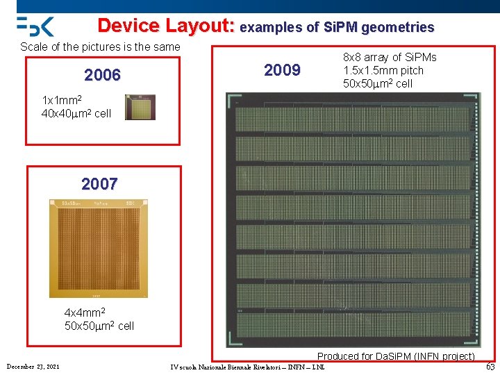
Device Layout: examples of Si. PM geometries Scale of the pictures is the same 2006 2009 8 x 8 array of Si. PMs 1. 5 x 1. 5 mm pitch 50 x 50 mm 2 cell 1 x 1 mm 2 40 x 40 mm 2 cell 2007 4 x 4 mm 2 50 x 50 mm 2 cell December 23, 2021 Produced for Da. Si. PM (INFN project) IV scuola Nazionale Biennale Rivelatori – INFN – LNL 63

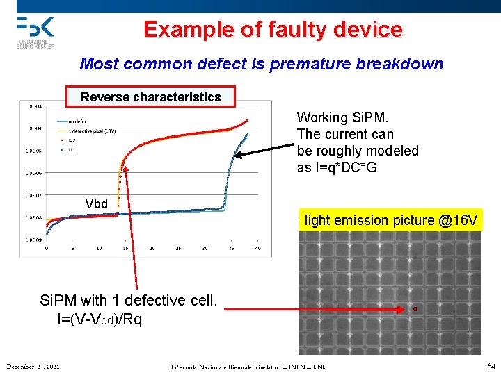
Example of faulty device Most common defect is premature breakdown Reverse characteristics Working Si. PM. The current can be roughly modeled as I=q*DC*G Vbd light emission picture @16 V Si. PM with 1 defective cell. I=(V-Vbd)/Rq December 23, 2021 IV scuola Nazionale Biennale Rivelatori – INFN – LNL 64

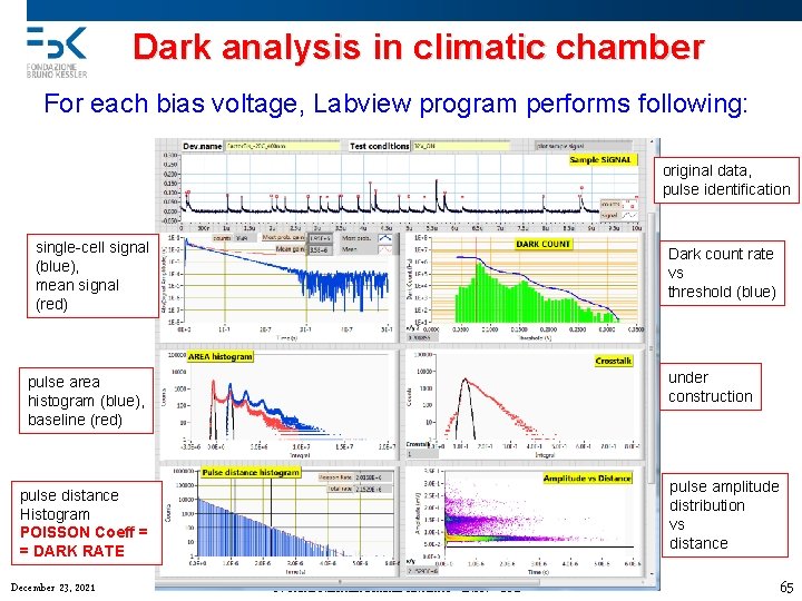
Dark analysis in climatic chamber For each bias voltage, Labview program performs following: original data, pulse identification single-cell signal (blue), mean signal (red) Dark count rate vs threshold (blue) under construction pulse area histogram (blue), baseline (red) pulse amplitude distribution vs distance pulse distance Histogram POISSON Coeff = = DARK RATE December 23, 2021 IV scuola Nazionale Biennale Rivelatori – INFN – LNL 65

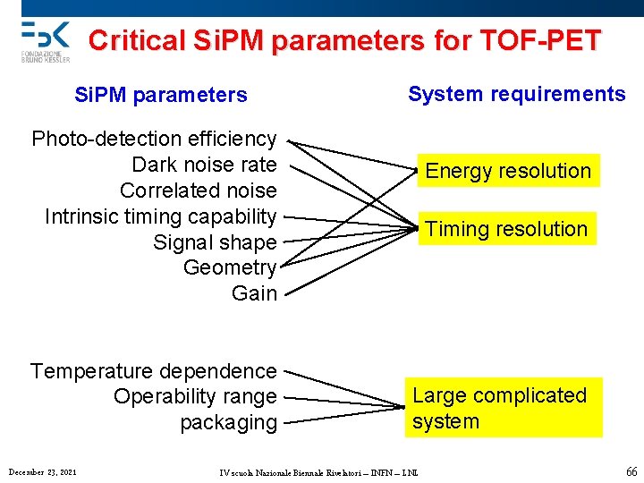
Critical Si. PM parameters for TOF-PET Si. PM parameters System requirements Photo-detection efficiency Dark noise rate Correlated noise Intrinsic timing capability Signal shape Geometry Gain Temperature dependence Operability range packaging December 23, 2021 Energy resolution Timing resolution Large complicated system IV scuola Nazionale Biennale Rivelatori – INFN – LNL 66
 Pirosilicato
 Estructura del silicio
 Silicio electrones de valencia
 Java introduzione
 Perche manzoni sceglie il seicento
 Introduzione a python
 Introduzione alla psicometria
 Grado totale di un monomio
 Reyneri introduzione alla sociologia del mercato del lavoro
 Pizza frazioni
 Conducibilita toroidale
 Sinalefe
 Struttura del vangelo di luca
 Introduzione alle funzioni
 Norma numero complesso
 Differenza abstract e introduzione
 Conclusione tesina razzismo
 Introduzione alla psicologia della comunicazione
 Introduzione alla geometria solida
 Tesina sulle donne introduzione
 Manuale di pedagogia generale
 Introduzione ai database
 Introduzione al calcolo letterale
 Introduzione alle criptovalute
 Introduzione alla sociologia ritzer
 Esempi di introduzione tesina terza media
 Testo informativo esempio svolto
 Introduzione alla psicologia della comunicazione
 Introduzione agli algoritmi e strutture dati
 I diritti umani: tesina
 Introduzione alle basi di dati
 Introduzione alla finanza
 Introduzione cap
 Pensiero complesso morin
 I promessi sposi autore
 Derivata ln
 Lettera commerciale data
 Che cos'è il testo poetico
 Introduzione caccia al tesoro
 Ciclo del carbonio schema
 Gentile ettore serra
 Boris groys volverse publico
 Cimo de uma montanha ou colina
 Calore specifico zanichelli
 Serra kamer
 Serra ertaylan
 In advertising
 Richard serra
 Serra de rodes
 Gráfico dente de serra
 Serra prayer for vocations
 Renata serra
 Sutura continua incavigliata
 Danila serra
 Dente de serra
 Richard serra
 Itc serra cesena
 Serra international inc
 James serra blog
 Inmon vs kimball
 La em cima daquela serra
 Cascina pizzo
 Richard serra verbs
 Francesc serra massansalvador
 Serra bülbül acar
 Fauna de la serra de tramuntana
 Richard serra charlie brown
