Interconnect Parasitic Extraction Speaker Wenjian Yu Tsinghua University

![Capacitance extraction Reference [1] W. Kao, C-Y. Lo, M. Basel and R. Singh, “Parasitic Capacitance extraction Reference [1] W. Kao, C-Y. Lo, M. Basel and R. Singh, “Parasitic](https://slidetodoc.com/presentation_image_h/037fad2b49c0596e458bc567bdf4d956/image-49.jpg)

![Inductance extraction Reference [1] M. W. Beattie and L. T. Pileggi, “Inductance 101: modeling Inductance extraction Reference [1] M. W. Beattie and L. T. Pileggi, “Inductance 101: modeling](https://slidetodoc.com/presentation_image_h/037fad2b49c0596e458bc567bdf4d956/image-78.jpg)
- Slides: 78

Interconnect Parasitic Extraction Speaker: Wenjian Yu Tsinghua University, Beijing, China Thanks to J. White, A. Nardi, W. Kao, L. T. Pileggi, Zhenhai Zhu

Outline Introduction to parasitic extraction n Resistance extraction n Capacitance extraction n n Inductance and impedance (RLC) extraction 2

Introduction to Parasitic Extraction 3

Introduction n Interconnect: conductive path n Ideally: wire only connects functional elements (devices, gates, blocks, …) and does not affect design performance n This assumption was approximately true for “large” design, it is unacceptable for DSM designs 4 Slides courtesy A. Nardi, UC Berkeley

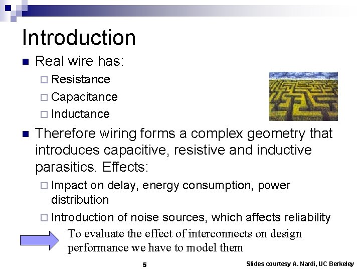
Introduction n Real wire has: ¨ Resistance ¨ Capacitance ¨ Inductance n Therefore wiring forms a complex geometry that introduces capacitive, resistive and inductive parasitics. Effects: ¨ Impact on delay, energy consumption, power distribution ¨ Introduction of noise sources, which affects reliability To evaluate the effect of interconnects on design performance we have to model them 5 Slides courtesy A. Nardi, UC Berkeley

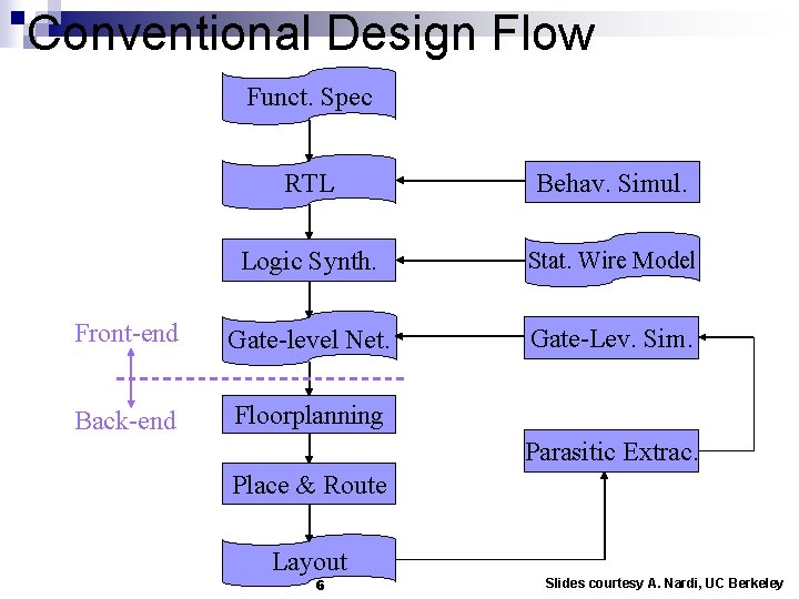
Conventional Design Flow Funct. Spec RTL Behav. Simul. Logic Synth. Stat. Wire Model Front-end Gate-level Net. Gate-Lev. Sim. Back-end Floorplanning Parasitic Extrac. Place & Route Layout 6 Slides courtesy A. Nardi, UC Berkeley

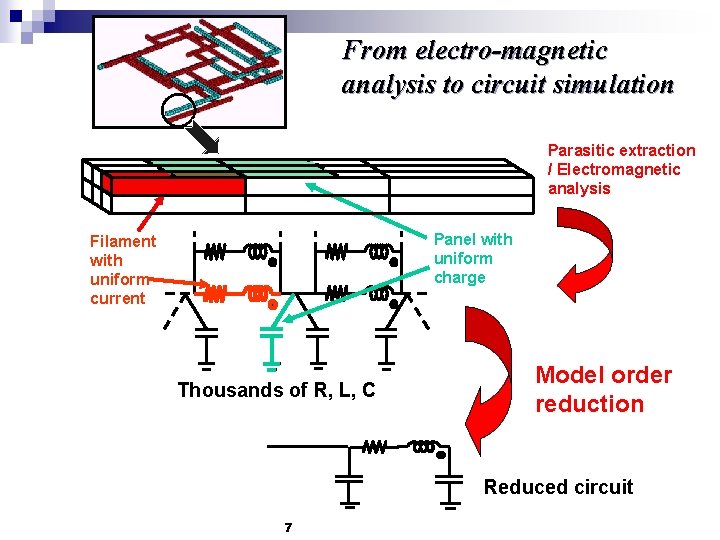
From electro-magnetic analysis to circuit simulation Parasitic extraction / Electromagnetic analysis Panel with uniform charge Filament with uniform current Thousands of R, L, C Model order reduction Reduced circuit 7

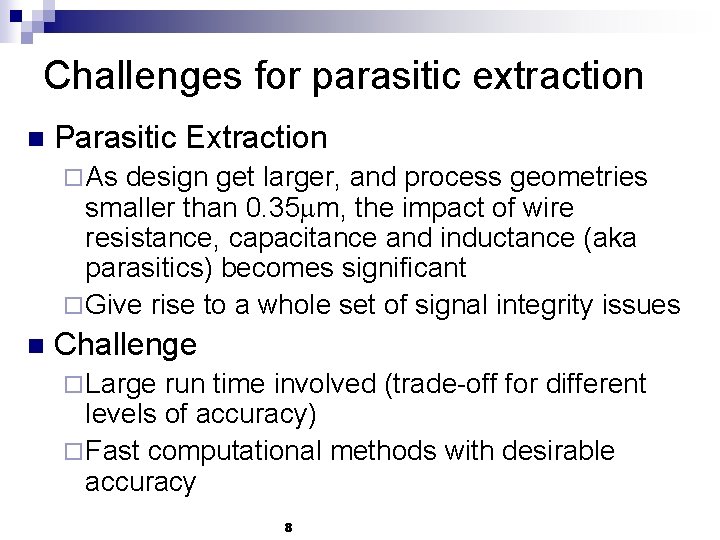
Challenges for parasitic extraction n Parasitic Extraction ¨ As design get larger, and process geometries smaller than 0. 35 m, the impact of wire resistance, capacitance and inductance (aka parasitics) becomes significant ¨ Give rise to a whole set of signal integrity issues n Challenge ¨ Large run time involved (trade-off for different levels of accuracy) ¨ Fast computational methods with desirable accuracy 8

Resistance Extraction 9

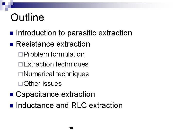
Outline Introduction to parasitic extraction n Resistance extraction n ¨ Problem formulation ¨ Extraction techniques ¨ Numerical techniques ¨ Other issues Capacitance extraction n Inductance and RLC extraction n 10

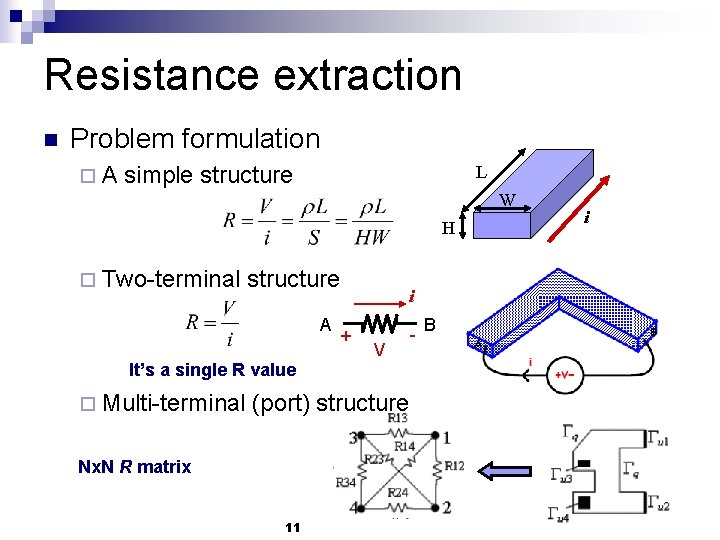
Resistance extraction n Problem formulation ¨A simple structure L W H ¨ Two-terminal structure A + i V It’s a single R value ¨ Multi-terminal (port) structure Nx. N R matrix 11 - B i

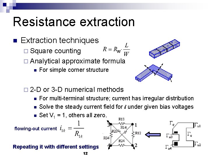
Resistance extraction n Extraction techniques ¨ Square counting ¨ Analytical approximate formula n For simple corner structure ¨ 2 -D n n n or 3 -D numerical methods For multi-terminal structure; current has irregular distribution Solve the steady current field for i under given bias voltages Set V 1 = 1, others all zero, flowing-out current Repeating it with different settings 12

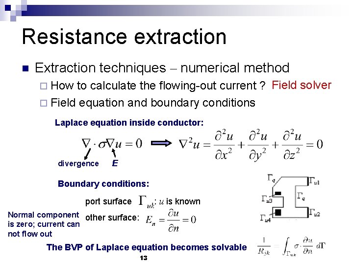
Resistance extraction n Extraction techniques – numerical method to calculate the flowing-out current ? Field solver ¨ Field equation and boundary conditions ¨ How Laplace equation inside conductor: divergence E Boundary conditions: : u is known port surface Normal component other surface: is zero; current can not flow out The BVP of Laplace equation becomes solvable 13

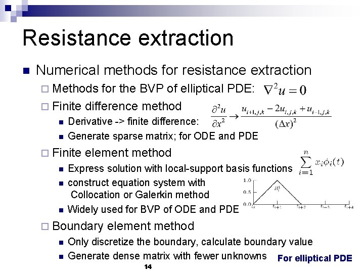
Resistance extraction n Numerical methods for resistance extraction ¨ Methods for the BVP of elliptical PDE: ¨ Finite difference method n n Derivative -> finite difference: Generate sparse matrix; for ODE and PDE ¨ Finite n n n element method Express solution with local-support basis functions construct equation system with Collocation or Galerkin method Widely used for BVP of ODE and PDE ¨ Boundary n n element method Only discretize the boundary, calculate boundary value Generate dense matrix with fewer unknowns For elliptical PDE 14

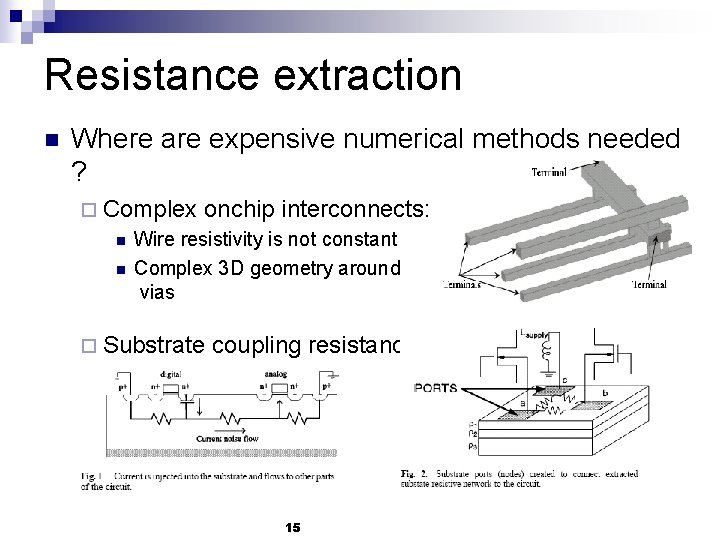
Resistance extraction n Where are expensive numerical methods needed ? ¨ Complex n n onchip interconnects: Wire resistivity is not constant Complex 3 D geometry around vias ¨ Substrate coupling resistance in mixed-signal IC 15

Resistance extraction n All these methods calculate DC resistance ¨ Suitable for analysis of local interconnects, or analysis under lower frequency ¨ High frequency: R of simple geometry estimated with skin depth; R of complex geometry extracted along with L n Reference W. Kao, C-Y. Lo, M. Basel and R. Singh, “Parasitic extraction: Current state of the art and future trends, ” Proceedings of IEEE, vol. 89, pp. 729 -739, 2001. ¨ Xiren Wang, Deyan Liu, Wenjian Yu and Zeyi Wang, "Improved boundary element method for fast 3 -D interconnect resistance extraction, " IEICE Trans. on Electronics, Vol. E 88 -C, No. 2, pp. 232240, Feb. 2005. ¨ 16

Capacitance Extraction 17

Outline Introduction to parasitic extraction n Resistance extraction n Capacitance extraction n ¨ Fundamentals and survey ¨ Volume discretization method ¨ Boundary element method ¨ Future issues n Inductance and RLC extraction 18

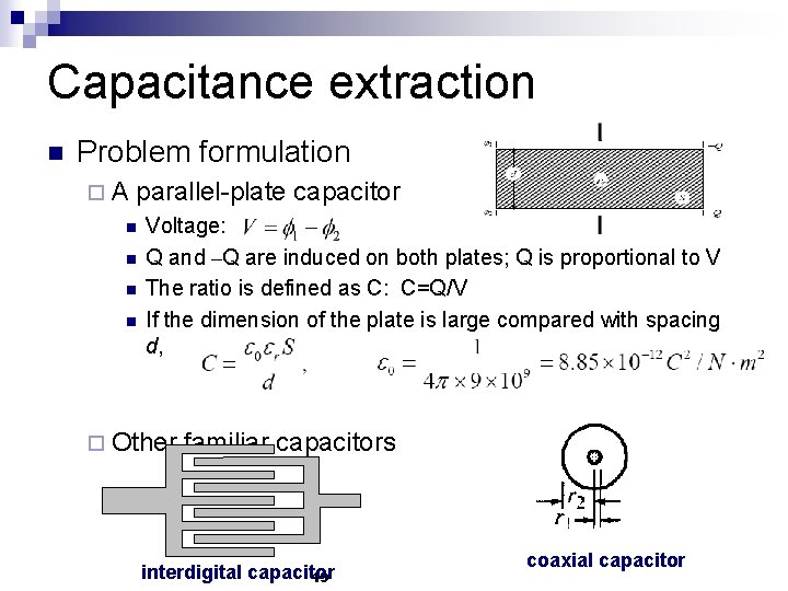
Capacitance extraction n Problem formulation ¨A parallel-plate capacitor n n Voltage: Q and –Q are induced on both plates; Q is proportional to V The ratio is defined as C: C=Q/V If the dimension of the plate is large compared with spacing d, ¨ Other familiar capacitors interdigital capacitor 19 coaxial capacitor

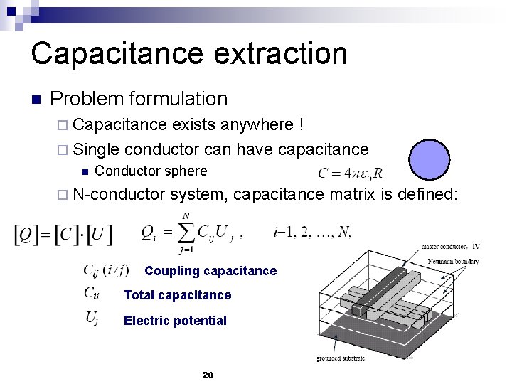
Capacitance extraction n Problem formulation ¨ Capacitance exists anywhere ! ¨ Single conductor can have capacitance n Conductor sphere ¨ N-conductor system, capacitance matrix is defined: Coupling capacitance Total capacitance Electric potential 20

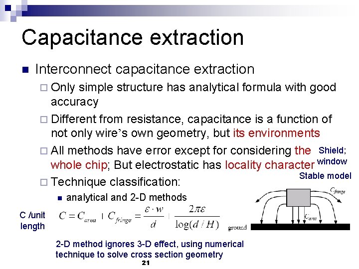
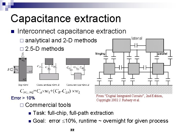
Capacitance extraction n Interconnect capacitance extraction ¨ Only simple structure has analytical formula with good accuracy ¨ Different from resistance, capacitance is a function of not only wire’s own geometry, but its environments ¨ All methods have error except for considering the Shield; whole chip; But electrostatic has locality character window Stable model ¨ Technique classification: n analytical and 2 -D methods C /unit length 2 -D method ignores 3 -D effect, using numerical technique to solve cross section geometry 21

Capacitance extraction n Interconnect capacitance extraction ¨ analytical and 2 -D methods ¨ 2. 5 -D methods Error > 10% ¨ Commercial n n tools lateral From “Digital Integrated Circuits”, 2 nd Edition, Copyright 2002 J. Rabaey et al. Task: full-chip, full-path extraction Goal: error 10%, runtime ~ overnight for given process 22

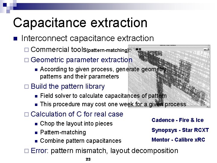
Capacitance extraction n Interconnect capacitance extraction ¨ Commercial tools(pattern-matching): ¨ Geometric parameter extraction n According to given process, generate geometry patterns and their parameters ¨ Build n n the pattern library Field solver to calculate capacitances of pattern This procedure may cost one week for a given process ¨ Calculation n of C for real case Chop the layout into pieces Pattern-matching Combine pattern capacitances ¨ Error: Cadence - Fire & Ice Synopsys - Star RCXT Mentor - Calibre x. RC pattern mismatch, layout decomposition 23

Capacitance extraction n 3 -D numerical methods ¨ Model actual geometry accurately; highest precision ¨ Shortage: capacity, running time ¨ Current status: widely investigated as research topic; used as library-building tool in industry, or for some special structures deserving high accuracy n Motivation ¨ The only golden value ¨ Increasing important as technology becomes complicated ¨ Algorithms for C extraction can be directly applied to R extraction; even extended to handle L extraction 24

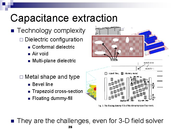
Capacitance extraction n Technology complexity ¨ Dielectric n n n Conformal dielectric Air void Multi-plane dielectric ¨ Metal n n configuration shape and type Bevel line Trapezoid cross-section Floating dummy-fill They are the challenges, even for 3 -D field solver 25

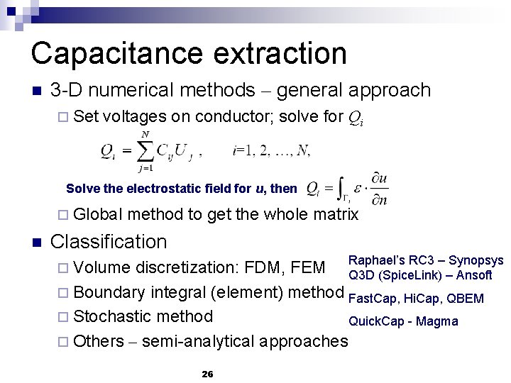
Capacitance extraction n 3 -D numerical methods – general approach ¨ Set voltages on conductor; solve for Qi Solve the electrostatic field for u, then ¨ Global n method to get the whole matrix Classification Raphael’s RC 3 – Synopsys ¨ Volume discretization: FDM, FEM Q 3 D (Spice. Link) – Ansoft ¨ Boundary integral (element) method Fast. Cap, Hi. Cap, QBEM ¨ Stochastic method Quick. Cap - Magma ¨ Others – semi-analytical approaches 26

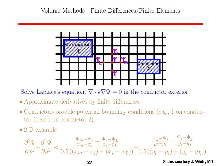
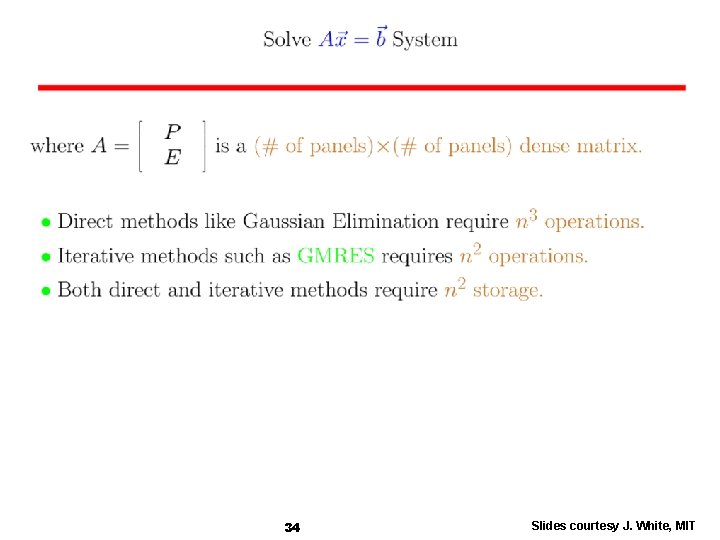
27 Slides courtesy J. White, MIT

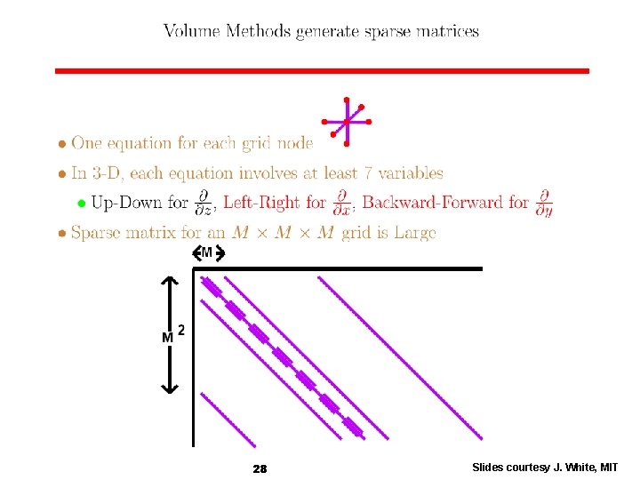
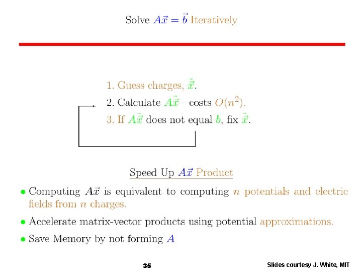
28 Slides courtesy J. White, MIT

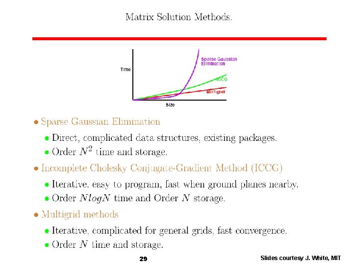
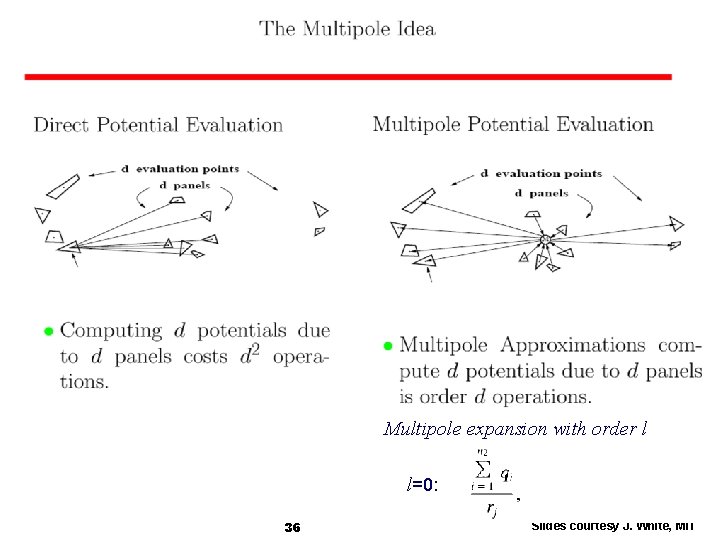
29 Slides courtesy J. White, MIT

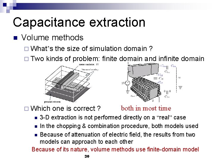
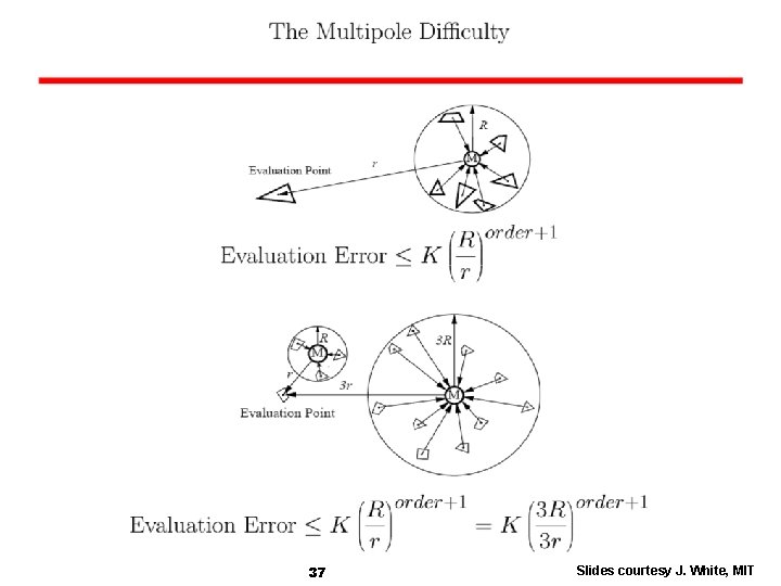
Capacitance extraction n Volume methods ¨ What’s the size of simulation domain ? ¨ Two kinds of problem: finite domain and infinite domain ¨ Which one is correct ? both in most time 3 -D extraction is not performed directly on a “real” case n In the chopping & combination procedure, both models used n Because of attenuation of electric field, the results from two models can approach to each other Because of its nature, volume methods use finite-domain model n 30

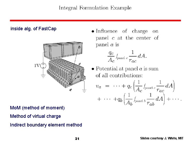
inside alg. of Fast. Cap c Mo. M (method of moment) Method of virtual charge Indirect boundary element method 31 Slides courtesy J. White, MIT

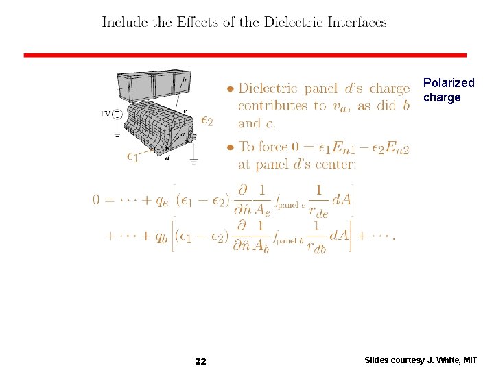
Polarized charge 32 Slides courtesy J. White, MIT

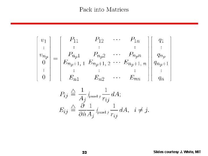
33 Slides courtesy J. White, MIT

34 Slides courtesy J. White, MIT

35 Slides courtesy J. White, MIT

Multipole expansion with order l l=0: 36 Slides courtesy J. White, MIT

37 Slides courtesy J. White, MIT

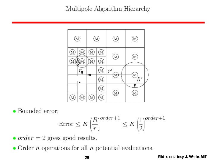
38 Slides courtesy J. White, MIT

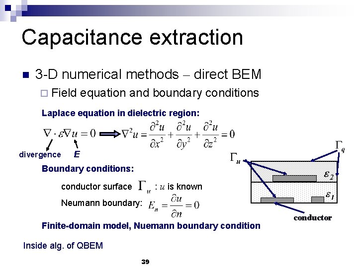
Capacitance extraction n 3 -D numerical methods – direct BEM ¨ Field equation and boundary conditions Laplace equation in dielectric region: divergence E Boundary conditions: : u is known conductor surface Neumann boundary: Finite-domain model, Nuemann boundary condition Inside alg. of QBEM 39 conductor

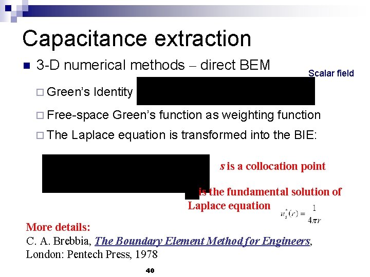
Capacitance extraction n 3 -D numerical methods – direct BEM ¨ Green’s Identity ¨ Free-space ¨ The Scalar field Green’s function as weighting function Laplace equation is transformed into the BIE: s is a collocation point is the fundamental solution of Laplace equation More details: C. A. Brebbia, The Boundary Element Method for Engineers, London: Pentech Press, 1978 40

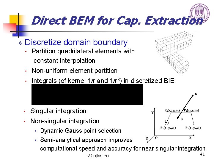
Direct BEM for Cap. Extraction v Discretize domain boundary • Partition quadrilateral elements with constant interpolation • Non-uniform element partition • Integrals (of kernel 1/r and 1/r 3) in discretized BIE: s • Singular integration • Non-singular integration j t • Dynamic Gauss point selection • Semi-analytical approach improves computational speed and accuracy for near singular integration Wenjian Yu 41

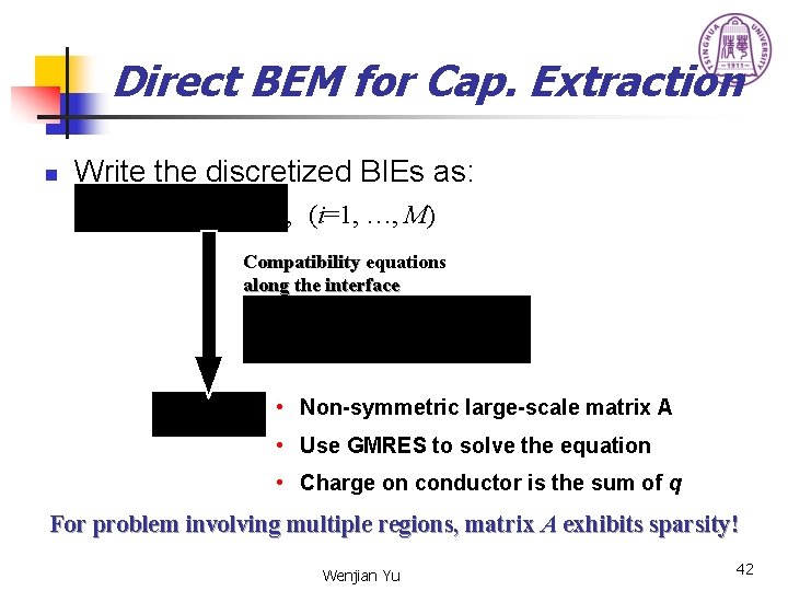
Direct BEM for Cap. Extraction n Write the discretized BIEs as: , (i=1, …, M) Compatibility equations along the interface • Non-symmetric large-scale matrix A • Use GMRES to solve the equation • Charge on conductor is the sum of q For problem involving multiple regions, matrix A exhibits sparsity! Wenjian Yu 42

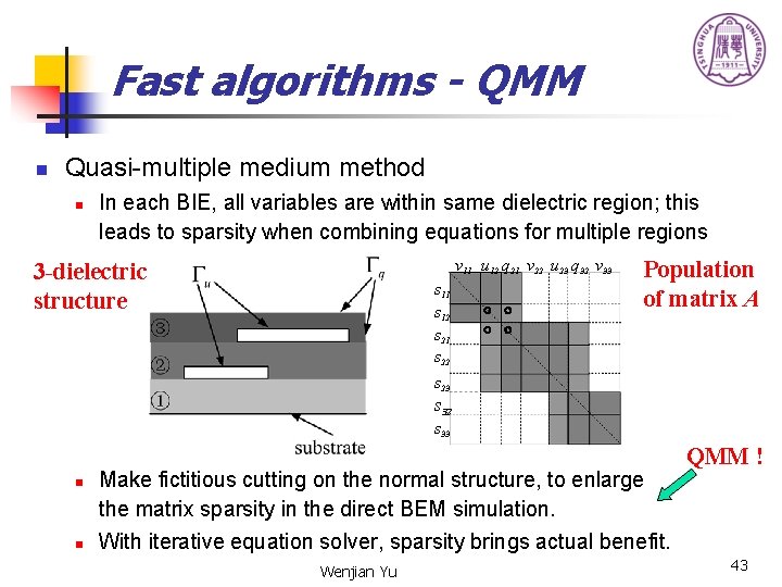
Fast algorithms - QMM n Quasi-multiple medium method n In each BIE, all variables are within same dielectric region; this leads to sparsity when combining equations for multiple regions v 11 u 12 q 21 v 22 u 23 q 32 v 33 3 -dielectric structure s 11 s 12 s 21 s 22 s 23 Population of matrix A s 32 s 33 n n Make fictitious cutting on the normal structure, to enlarge the matrix sparsity in the direct BEM simulation. With iterative equation solver, sparsity brings actual benefit. Wenjian Yu QMM ! 43

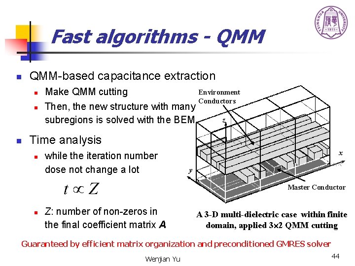
Fast algorithms - QMM n QMM-based capacitance extraction n Make QMM cutting Then, the new structure with many subregions is solved with the BEM Environment Conductors z Time analysis n while the iteration number dose not change a lot x y Master Conductor n Z: number of non-zeros in the final coefficient matrix A A 3 -D multi-dielectric case within finite domain, applied 3 2 QMM cutting Guaranteed by efficient matrix organization and preconditioned GMRES solver Wenjian Yu 44

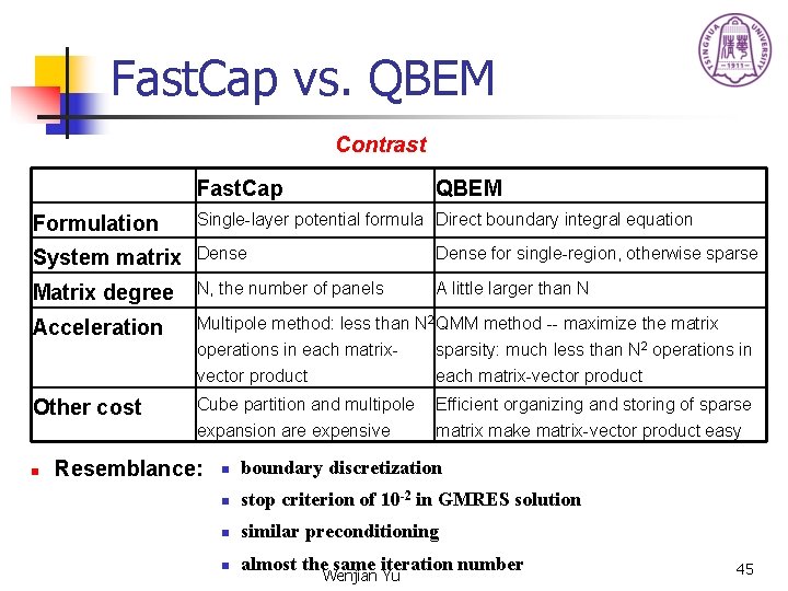
Fast. Cap vs. QBEM Contrast Fast. Cap QBEM Formulation Single-layer potential formula Direct boundary integral equation System matrix Dense for single-region, otherwise sparse Matrix degree N, the number of panels A little larger than N Acceleration Multipole method: less than N 2 QMM method -- maximize the matrix operations in each matrixsparsity: much less than N 2 operations in Other cost n vector product each matrix-vector product Cube partition and multipole expansion are expensive Efficient organizing and storing of sparse matrix make matrix-vector product easy Resemblance: n boundary discretization n stop criterion of 10 -2 in GMRES solution n similar preconditioning n almost the same iteration number Wenjian Yu 45

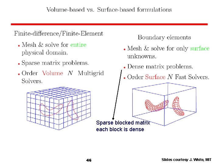
Sparse blocked matrix each block is dense 46 Slides courtesy J. White, MIT

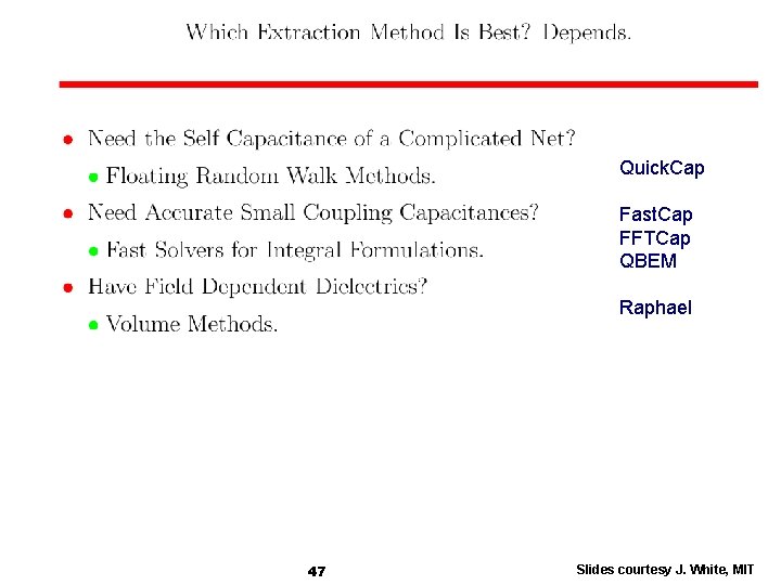
Quick. Cap Fast. Cap FFTCap QBEM Raphael 47 Slides courtesy J. White, MIT

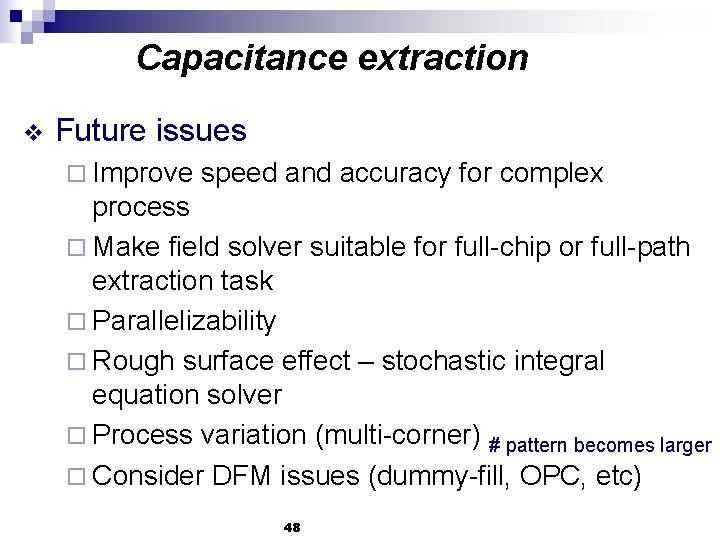
Capacitance extraction v Future issues o Improve speed and accuracy for complex process o Make field solver suitable for full-chip or full-path extraction task o Parallelizability o Rough surface effect – stochastic integral equation solver o Process variation (multi-corner) # pattern becomes larger o Consider DFM issues (dummy-fill, OPC, etc) 48
![Capacitance extraction Reference 1 W Kao CY Lo M Basel and R Singh Parasitic Capacitance extraction Reference [1] W. Kao, C-Y. Lo, M. Basel and R. Singh, “Parasitic](https://slidetodoc.com/presentation_image_h/037fad2b49c0596e458bc567bdf4d956/image-49.jpg)
Capacitance extraction Reference [1] W. Kao, C-Y. Lo, M. Basel and R. Singh, “Parasitic extraction: Current state of the art and future trends, ” Proceedings of IEEE, vol. 89, pp. 729 -739, 2001. [2] Wenjian Yu and Zeyi Wang, “Capacitance extraction”, in Encyclopedia of RF and Microwave Engineering , K. Chang [Eds. ], John Wiley & Sons Inc. , 2005, pp. 565576. [3] K. Nabors and J. White, Fast. Cap: A multipole accelerated 3 -D capacitance extraction program, IEEE Trans. Computer-Aided Design, 10(11): 1447 -1459, 1991. [4] Y. L. Le Coz and R. B. Iverson, “A stochastic algorithm for high speed capacitance extraction in integrated circuits, ” Solid State Electronics, 35(7): 1005 -1012, 1992. [5] J. R. Phillips and J. White, “A precorrected-FFT method for electrostatic analysis of complicated 3 -D structures, ” IEEE Trans. Computer-Aided Design, 16(10): 10591072, 1997 [6] W. Shi, J. Liu, N. Kakani and T. Yu, A fast hierarchical algorithm for threedimensional capacitance extraction, IEEE Trans. Computer-Aided Design, 21(3): 330 -336, 2002. [7] W. Yu, Z. Wang and J. Gu, Fast capacitance extraction of actual 3 -D VLSI interconnects using quasi-multiple medium accelerated BEM, IEEE Trans. Microwave Theory Tech. , 51(1): 109 -120, 2003. [8] W. Shi and F. Yu, A divide-and-conquer algorithm for 3 -D capacitance extraction, IEEE Trans. Computer-Aided Design, 23(8): 1157 -1163, 2004. 49

Inductance Extraction 50

Outline n Basic ¨ Two laws about inductive interaction ¨ Loop inductance n Onchip inductance extraction ¨ Partial inductance & PEEC model ¨ Frequency-dependent LR extraction Fast. Henry n Inductance or full-wave extraction with BEM ¨ Maxwell equations & assumptions ¨ Boundary element method 51

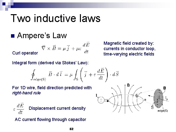
Two inductive laws n Ampere’s Law Magnetic field created by: currents in conductor loop, time-varying electric fields Curl operator Integral form (derived via Stokes’ Law): For 1 D wire, field direction predicted with right-hand rule Displacement current density AC current flowing through capacitor 52

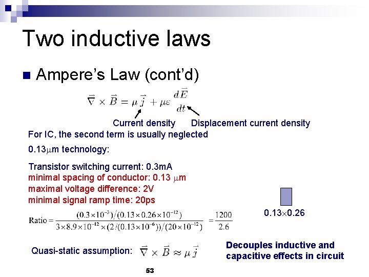
Two inductive laws n Ampere’s Law (cont’d) Current density Displacement current density For IC, the second term is usually neglected 0. 13 m technology: Transistor switching current: 0. 3 m. A minimal spacing of conductor: 0. 13 m maximal voltage difference: 2 V minimal signal ramp time: 20 ps 0. 13 0. 26 Decouples inductive and capacitive effects in circuit Quasi-static assumption: 53

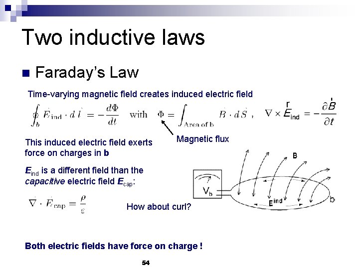
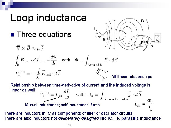
Two inductive laws n Faraday’s Law Time-varying magnetic field creates induced electric field This induced electric field exerts force on charges in b Magnetic flux Eind is a different field than the capacitive electric field Ecap: How about curl? Both electric fields have force on charge ! 54

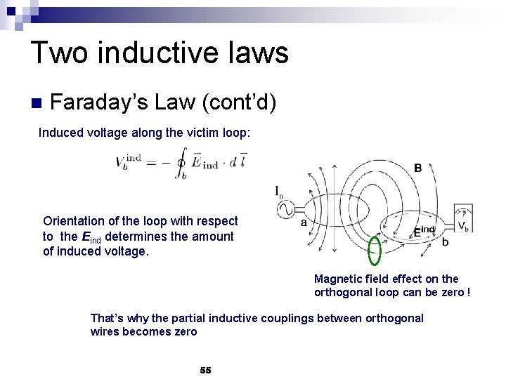
Two inductive laws n Faraday’s Law (cont’d) Induced voltage along the victim loop: Orientation of the loop with respect to the Eind determines the amount of induced voltage. Magnetic field effect on the orthogonal loop can be zero ! That’s why the partial inductive couplings between orthogonal wires becomes zero 55

Loop inductance n Three equations All linear relationships Relationship between time-derivative of current and the induced voltage is linear as well: Mutual inductance; self inductance if a=b There are inductors in IC as components of filter or oscillator circuits; There also inductors not deliberately designed into IC, i. e. parasitic inductance 56

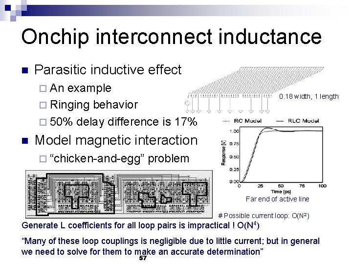
Onchip interconnect inductance n Parasitic inductive effect ¨ An example ¨ Ringing behavior ¨ 50% delay difference is 17% n 0. 18 width, 1 length Model magnetic interaction ¨ “chicken-and-egg” problem Far end of active line # Possible current loop: O(N 2) Generate L coefficients for all loop pairs is impractical ! O(N 4) “Many of these loop couplings is negligible due to little current; but in general we need to solve for them to make an accurate determination” 57

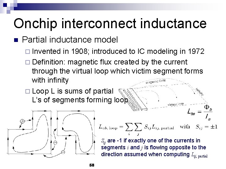
Onchip interconnect inductance n Partial inductance model ¨ Invented in 1908; introduced to IC modeling in 1972 ¨ Definition: magnetic flux created by the current through the virtual loop which victim segment forms with infinity ¨ Loop L is sums of partial L’s of segments forming loop Sij are -1 if exactly one of the currents in segments i and j is flowing opposite to the direction assumed when computing Lij, partial 58

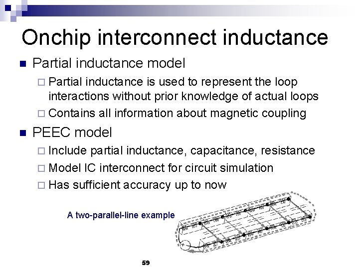
Onchip interconnect inductance n Partial inductance model ¨ Partial inductance is used to represent the loop interactions without prior knowledge of actual loops ¨ Contains all information about magnetic coupling n PEEC model ¨ Include partial inductance, capacitance, resistance ¨ Model IC interconnect for circuit simulation ¨ Has sufficient accuracy up to now A two-parallel-line example 59

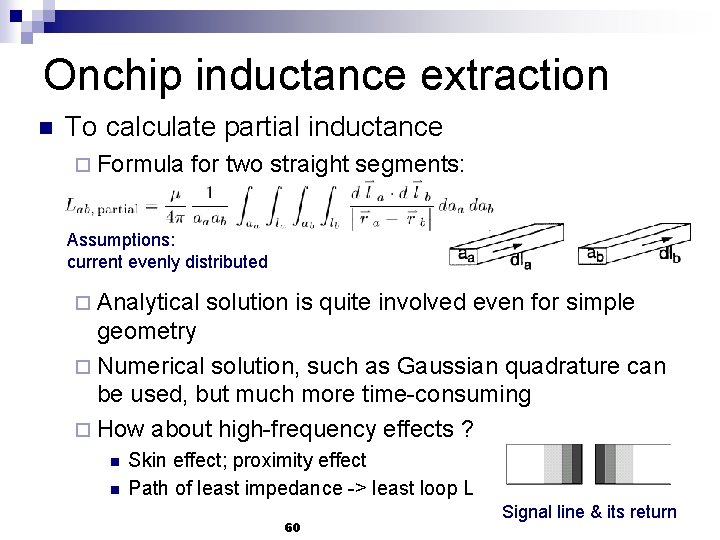
Onchip inductance extraction n To calculate partial inductance ¨ Formula for two straight segments: Assumptions: current evenly distributed ¨ Analytical solution is quite involved even for simple geometry ¨ Numerical solution, such as Gaussian quadrature can be used, but much more time-consuming ¨ How about high-frequency effects ? n n Skin effect; proximity effect Path of least impedance -> least loop L 60 Signal line & its return

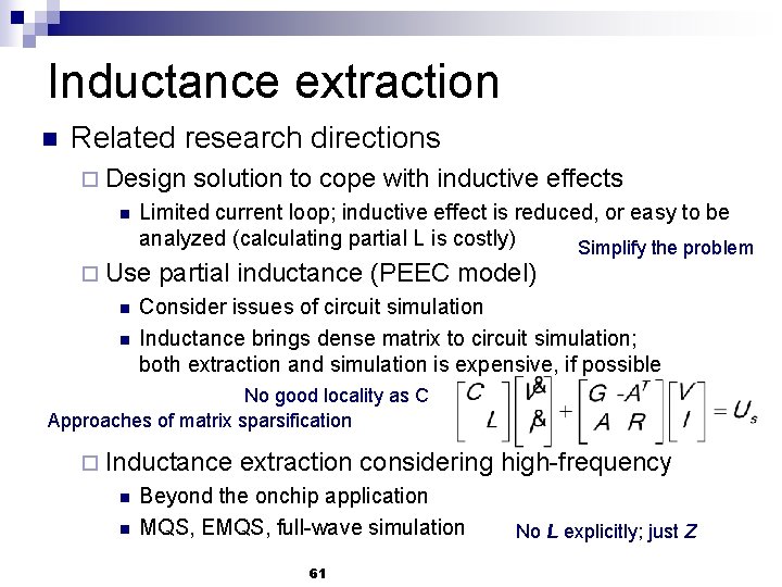
Inductance extraction n Related research directions ¨ Design n Limited current loop; inductive effect is reduced, or easy to be analyzed (calculating partial L is costly) Simplify the problem ¨ Use n n solution to cope with inductive effects partial inductance (PEEC model) Consider issues of circuit simulation Inductance brings dense matrix to circuit simulation; both extraction and simulation is expensive, if possible No good locality as C Approaches of matrix sparsification ¨ Inductance n n extraction considering high-frequency Beyond the onchip application MQS, EMQS, full-wave simulation 61 No L explicitly; just Z

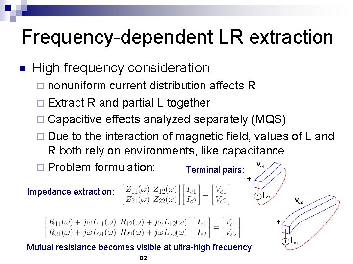
Frequency-dependent LR extraction n High frequency consideration ¨ nonuniform current distribution affects R ¨ Extract R and partial L together ¨ Capacitive effects analyzed separately (MQS) ¨ Due to the interaction of magnetic field, values of L and R both rely on environments, like capacitance ¨ Problem formulation: Terminal pairs: Impedance extraction: Mutual resistance becomes visible at ultra-high frequency 62

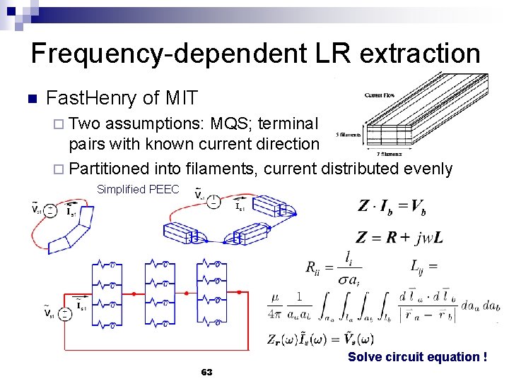
Frequency-dependent LR extraction n Fast. Henry of MIT ¨ Two assumptions: MQS; terminal pairs with known current direction ¨ Partitioned into filaments, current distributed evenly Simplified PEEC Solve circuit equation ! 63

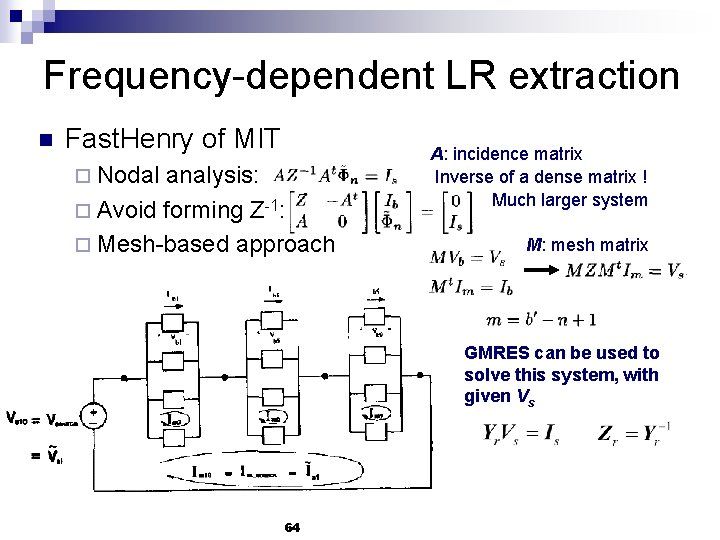
Frequency-dependent LR extraction n Fast. Henry of MIT ¨ Nodal analysis: ¨ Avoid forming Z-1: ¨ Mesh-based approach A: incidence matrix Inverse of a dense matrix ! Much larger system M: mesh matrix GMRES can be used to solve this system, with given Vs 64

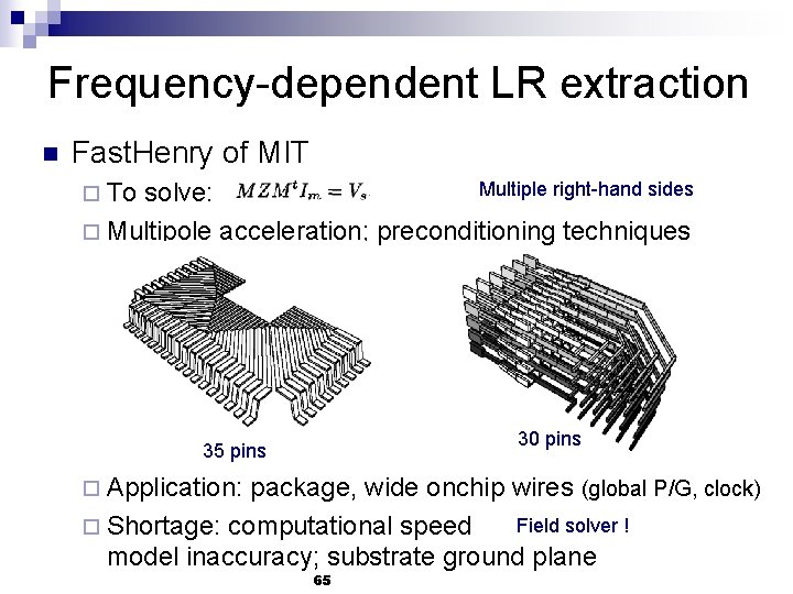
Frequency-dependent LR extraction n Fast. Henry of MIT Multiple right-hand sides solve: ¨ Multipole acceleration; preconditioning techniques ¨ To 30 pins 35 pins ¨ Application: package, wide onchip wires (global P/G, clock) Field solver ! ¨ Shortage: computational speed model inaccuracy; substrate ground plane 65

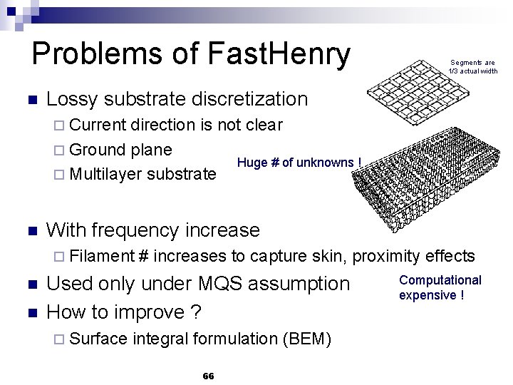
Problems of Fast. Henry n Segments are 1/3 actual width Lossy substrate discretization ¨ Current direction is not clear ¨ Ground plane Huge # of unknowns ! ¨ Multilayer substrate n With frequency increase ¨ Filament n n # increases to capture skin, proximity effects Used only under MQS assumption How to improve ? ¨ Surface integral formulation (BEM) 66 Computational expensive !

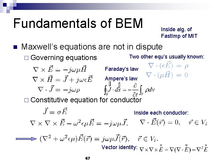
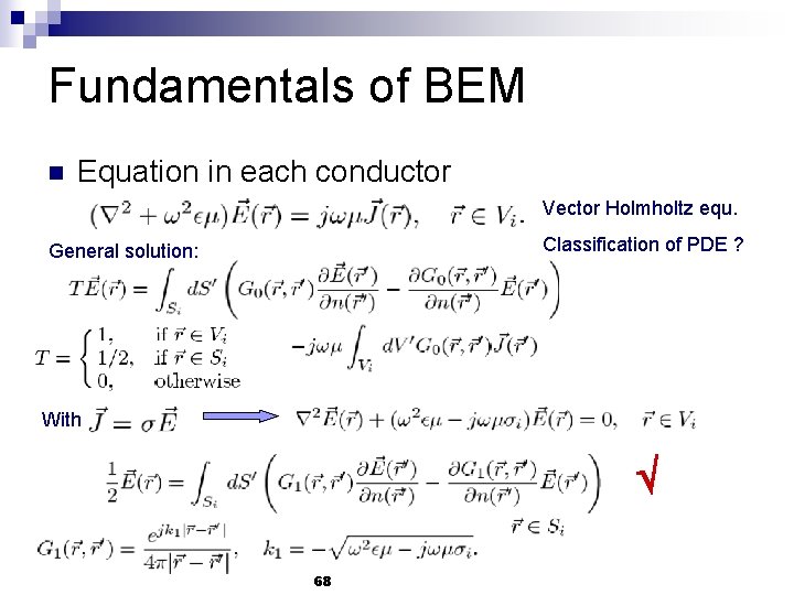
Fundamentals of BEM n Inside alg. of Fast. Imp of MIT Maxwell’s equations are not in dispute ¨ Governing equations Two other equ’s usually known: Faraday’s law Ampere’s law ¨ Constitutive equation for conductor Inside each conductor: Vector identity: 67

Fundamentals of BEM n Equation in each conductor Vector Holmholtz equ. Classification of PDE ? General solution: With 68

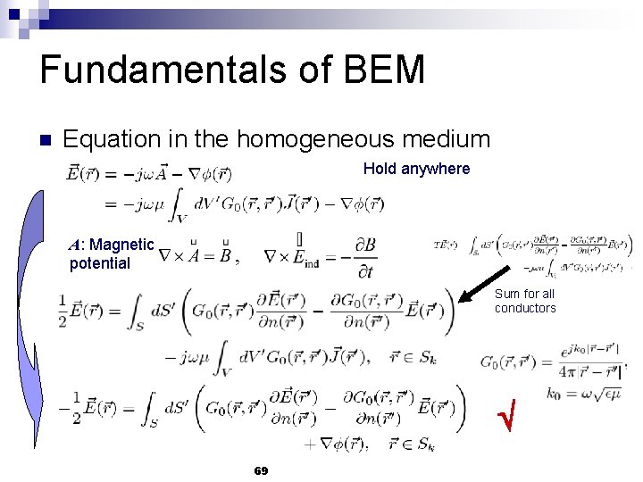
Fundamentals of BEM n Equation in the homogeneous medium Hold anywhere A: Magnetic potential Sum for all conductors 69

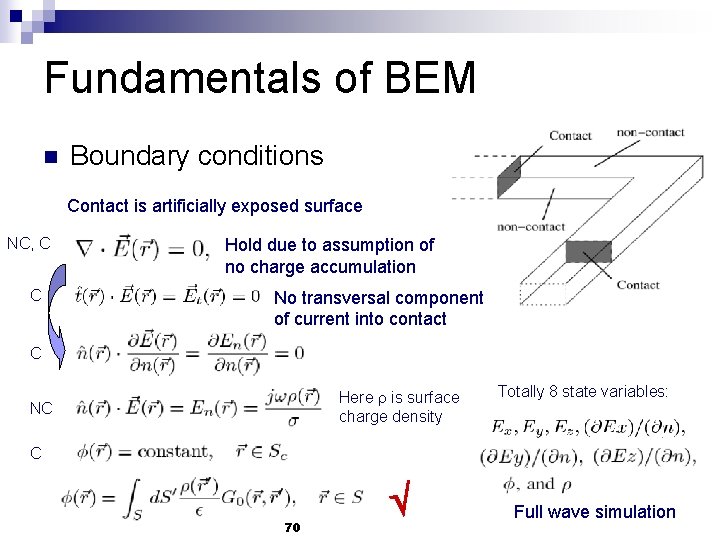
Fundamentals of BEM n Boundary conditions Contact is artificially exposed surface NC, C C Hold due to assumption of no charge accumulation No transversal component of current into contact C Here is surface charge density NC Totally 8 state variables: C 70 Full wave simulation

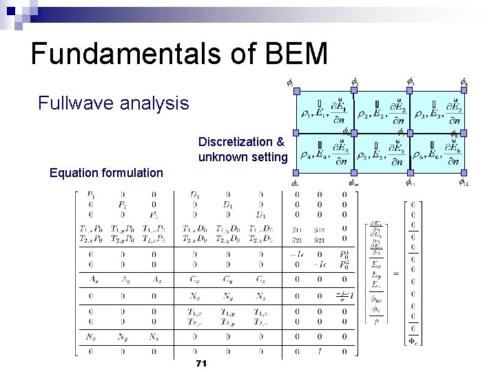
Fundamentals of BEM Fullwave analysis Discretization & unknown setting Equation formulation 71

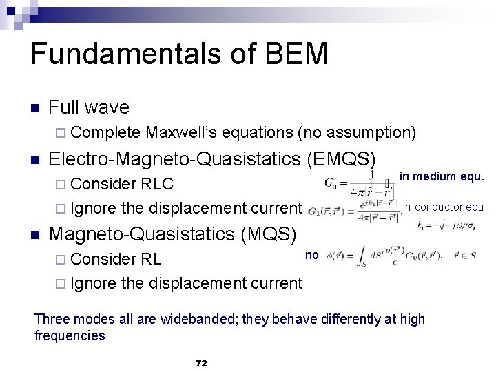
Fundamentals of BEM n Full wave ¨ Complete n Maxwell’s equations (no assumption) Electro-Magneto-Quasistatics (EMQS) ¨ Consider RLC ¨ Ignore the displacement current n in medium equ. in conductor equ. Magneto-Quasistatics (MQS) no RL ¨ Ignore the displacement current ¨ Consider Three modes all are widebanded; they behave differently at high frequencies 72

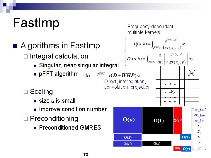
Fast. Imp n Frequency-dependent multiple kernels Algorithms in Fast. Imp ¨ Integral n n calculation Singular, near-singular integral p. FFT algorithm Direct, interpolation, convolution, projection ¨ Scaling n n size u is small Improve condition number ¨ Preconditioning n Preconditioned GMRES 73

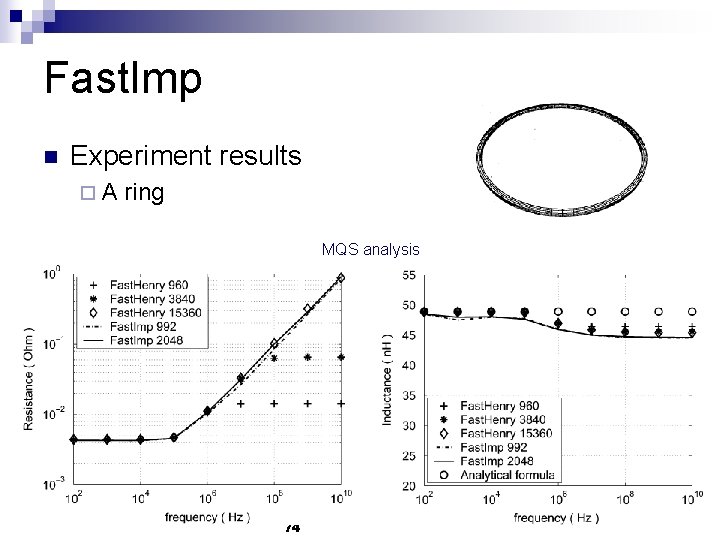
Fast. Imp n Experiment results ¨A ring MQS analysis 74

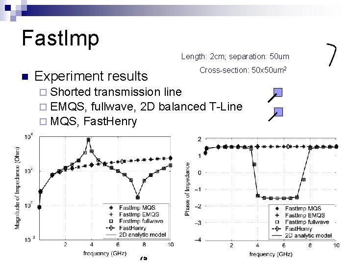
Fast. Imp Length: 2 cm; separation: 50 um n Experiment results ¨ Shorted Cross-section: 50 x 50 um 2 transmission line ¨ EMQS, fullwave, 2 D balanced T-Line ¨ MQS, Fast. Henry 75

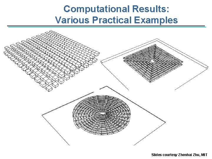
Computational Results: Various Practical Examples Slides courtesy Zhenhai Zhu, MIT

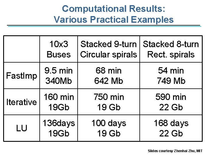
Computational Results: Various Practical Examples 10 x 3 Buses Stacked 9 -turn Stacked 8 -turn Circular spirals Rect. spirals 9. 5 min Fast. Imp 340 Mb 68 min 642 Mb 54 min 749 Mb 160 min Iterative 19 Gb 750 min 19 Gb 590 min 22 Gb 136 days 19 Gb 100 days 19 Gb 168 days 22 Gb LU Slides courtesy Zhenhai Zhu, MIT
![Inductance extraction Reference 1 M W Beattie and L T Pileggi Inductance 101 modeling Inductance extraction Reference [1] M. W. Beattie and L. T. Pileggi, “Inductance 101: modeling](https://slidetodoc.com/presentation_image_h/037fad2b49c0596e458bc567bdf4d956/image-78.jpg)
Inductance extraction Reference [1] M. W. Beattie and L. T. Pileggi, “Inductance 101: modeling and extraction, ” in Proc. Design Automation Conference, pp. 323 -328, June 2001. [2] M. Kamon, M. J. Tsuk, and J. K. White, “Fasthenry: a multipoleaccelerated 3 -D inductance extraction program, ” IEEE Trans. Microwave Theory Tech. , pp. 1750 - 1758, Sep 1994. [3] Z. Zhu, B. Song, and J. White. Algorithms in Fastimp: a fast and wideband impedance extraction program for complicated 3 -D geometries. IEEE Trans. Computer-Aided Design, 24(7): 981 -998, July 2005. [4] W. Kao, C-Y. Lo, M. Basel and R. Singh, “Parasitic extraction: Current state of the art and future trends, ” Proceedings of IEEE, vol. 89, pp. 729 -739, 2001. [5] http: //www. rle. mit. edu/cpg/research_codes. htm (Fast. Cap, Fast. Henry, Fast. Imp) 78