High AverageEfficiency Power Amplifier Techniques Jason Stauth U
![References • • • [1] A. Jerng and C. G. Sodini, "A Wideband Delta-Sigma References • • • [1] A. Jerng and C. G. Sodini, "A Wideband Delta-Sigma](https://slidetodoc.com/presentation_image/4ce9a8e411d42aae6e45f7f09074f287/image-44.jpg)
- Slides: 44

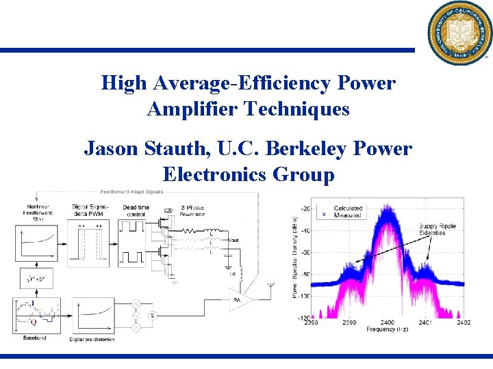
High Average-Efficiency Power Amplifier Techniques Jason Stauth, U. C. Berkeley Power Electronics Group

Overview • Application Space: Efficient RF Power Amplifiers • PA Fundamentals, Polar/ET Architectures • Challenges with Polar/ET • Research Directions • Direct Digital Modulation • Pulse-Density Modulation

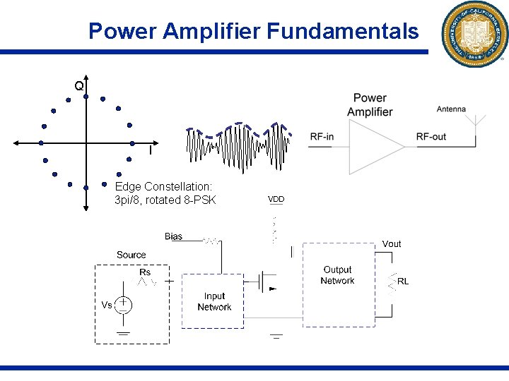
Power Amplifier Fundamentals Q I Edge Constellation: 3 pi/8, rotated 8 -PSK

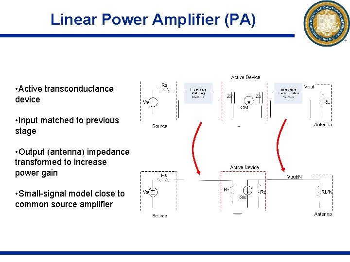
Linear Power Amplifier (PA) • Active transconductance device • Input matched to previous stage • Output (antenna) impedance transformed to increase power gain • Small-signal model close to common source amplifier

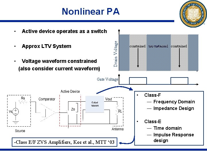
• Active device operates as a switch • Approx LTV System • Voltage waveform constrained (also consider current waveform) Drain Voltage Nonlinear PA constrained unconstrained Gate Voltage -Class E/F ZVS Amplifiers, Kee et al. , MTT ‘ 03 • Class-F — Frequency Domain — Impedance Design • Class-E — Time domain — Impulse Response design

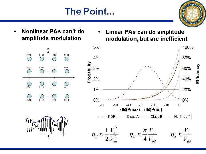
The Point… • Nonlinear PAs can’t do amplitude modulation • Linear PAs can do amplitude modulation, but are inefficient

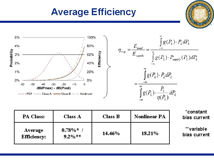
Average Efficiency PA Class: Class A Average Efficiency: 0. 78%* / 9. 2%** Class B 14. 46% Nonlinear PA *constant bias current 18. 21% **variable bias current

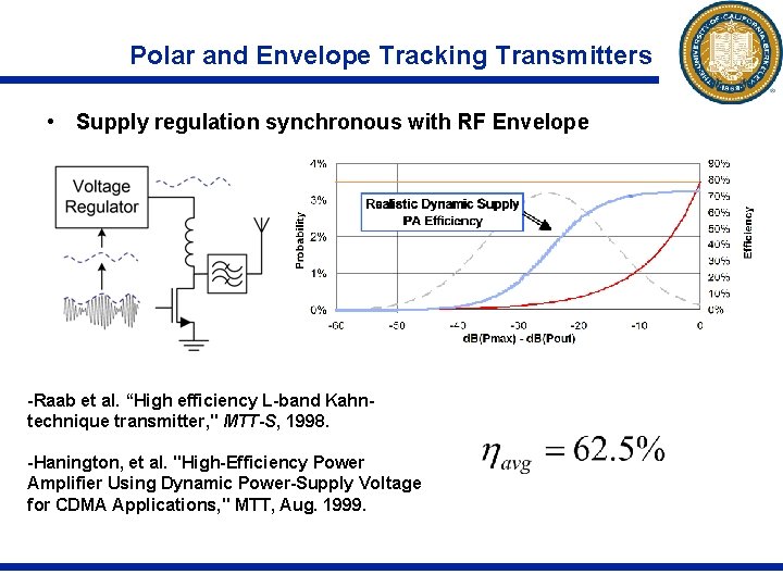
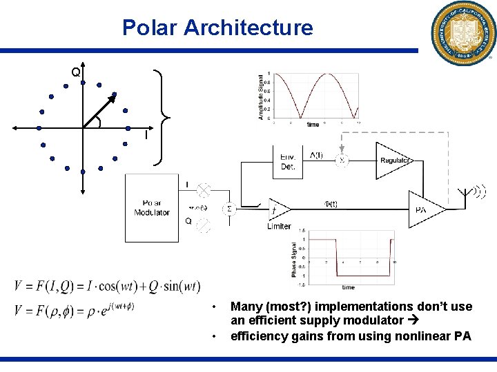
Polar and Envelope Tracking Transmitters • Supply regulation synchronous with RF Envelope -Raab et al. “High efficiency L-band Kahntechnique transmitter, " MTT-S, 1998. -Hanington, et al. "High-Efficiency Power Amplifier Using Dynamic Power-Supply Voltage for CDMA Applications, " MTT, Aug. 1999.

Polar Architecture Q I • • Many (most? ) implementations don’t use an efficient supply modulator efficiency gains from using nonlinear PA

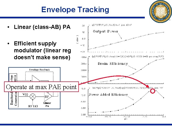
Envelope Tracking • Linear (class-AB) PA • Efficient supply modulator (linear reg doesn’t make sense) Operate at max PAE point

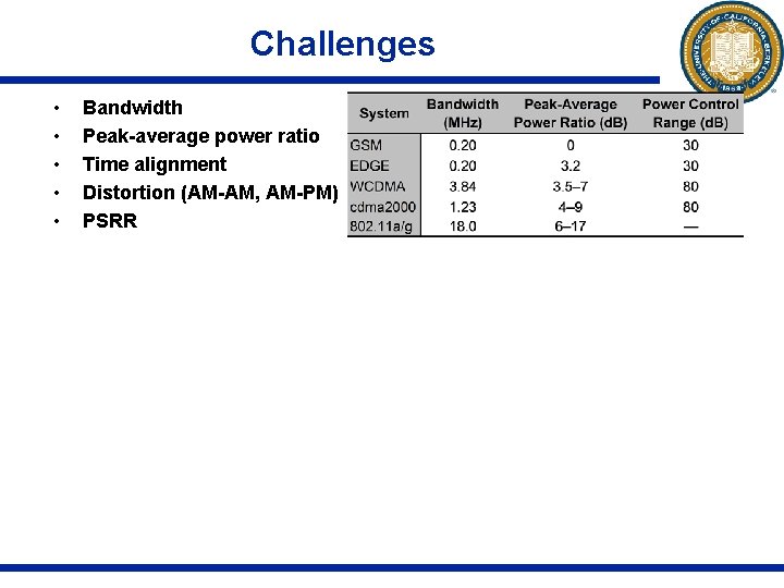
Challenges • • • Bandwidth Peak-average power ratio Time alignment Distortion (AM-AM, AM-PM) PSRR

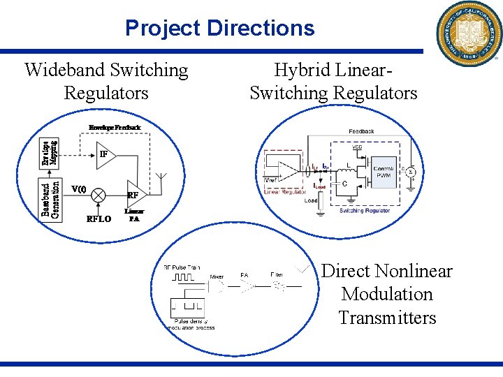
Project Directions Wideband Switching Regulators Hybrid Linear. Switching Regulators Direct Nonlinear Modulation Transmitters

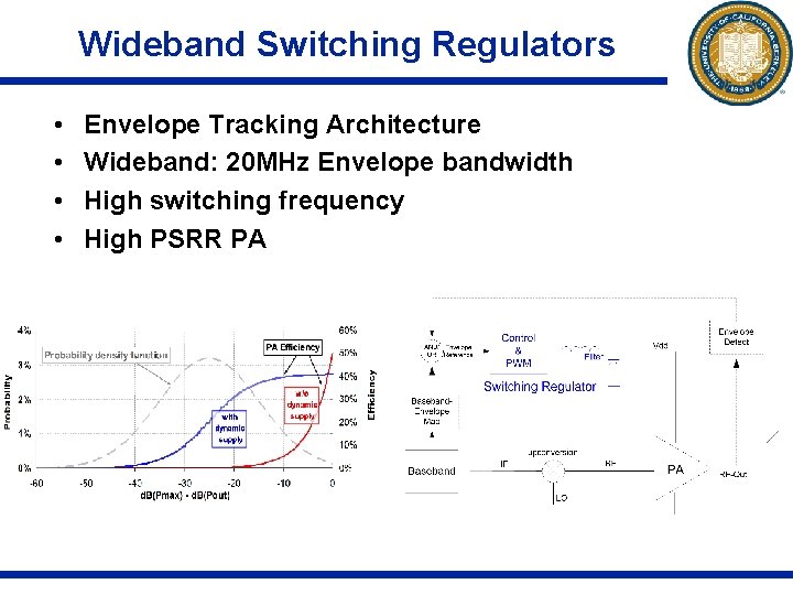
Wideband Switching Regulators • • Envelope Tracking Architecture Wideband: 20 MHz Envelope bandwidth High switching frequency High PSRR PA

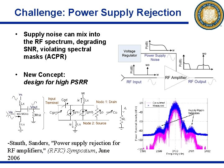
Challenge: Power Supply Rejection • Supply noise can mix into the RF spectrum, degrading SNR, violating spectral masks (ACPR) • New Concept: design for high PSRR -Stauth, Sanders, "Power supply rejection for RF amplifiers, " (RFIC) Symposium, June 2006

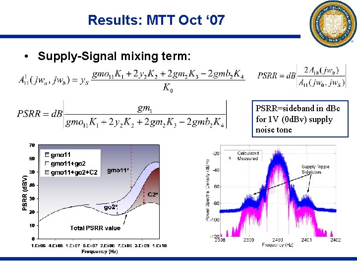
Results: MTT Oct ‘ 07 • Supply-Signal mixing term: PSRR=sideband in d. Bc for 1 V (0 d. Bv) supply noise tone

Hybrid Linear-Switching Regulators

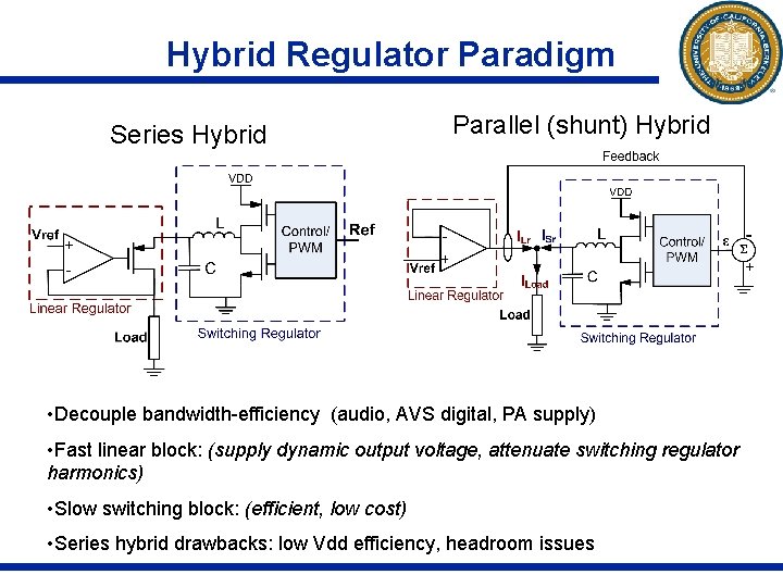
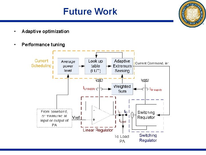
Hybrid Regulator Paradigm Series Hybrid Parallel (shunt) Hybrid • Decouple bandwidth-efficiency (audio, AVS digital, PA supply) • Fast linear block: (supply dynamic output voltage, attenuate switching regulator harmonics) • Slow switching block: (efficient, low cost) • Series hybrid drawbacks: low Vdd efficiency, headroom issues

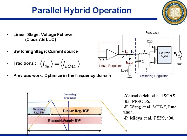
Parallel Hybrid Operation • Linear Stage: Voltage Follower (Class AB LDO) • Switching Stage: Current source • Traditional: • Previous work: Optimize in the frequency domain -Yousefzadeh, et al. ISCAS ‘ 05, PESC 06. -F. Wang et al, MTT-S, June 2004. -P. Midya et al. PESC, ‘ 00.

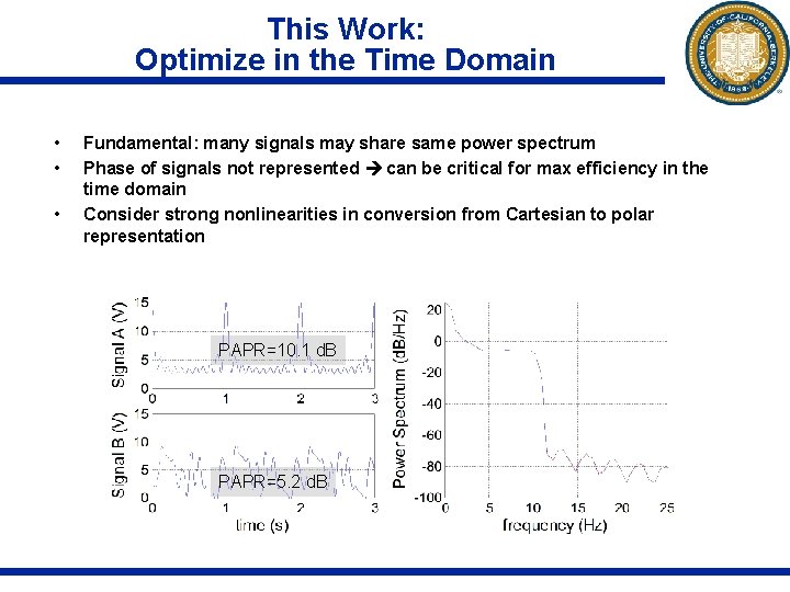
This Work: Optimize in the Time Domain • • • Fundamental: many signals may share same power spectrum Phase of signals not represented can be critical for max efficiency in the time domain Consider strong nonlinearities in conversion from Cartesian to polar representation PAPR=10. 1 d. B PAPR=5. 2 d. B

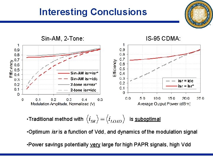
Interesting Conclusions Sin-AM, 2 -Tone: • Traditional method with IS-95 CDMA: is suboptimal • Optimum isr is a function of Vdd, and dynamics of the modulation signal • Power savings potentially very large for high PAPR signals, high Vdd

Future Work • Adaptive optimization • Performance tuning

Digital Pulse-Density Modulation

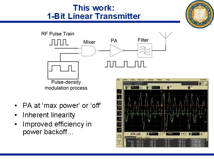
This work: 1 -Bit Linear Transmitter • PA at ‘max power’ or ‘off’ • Inherent linearity • Improved efficiency in power backoff…

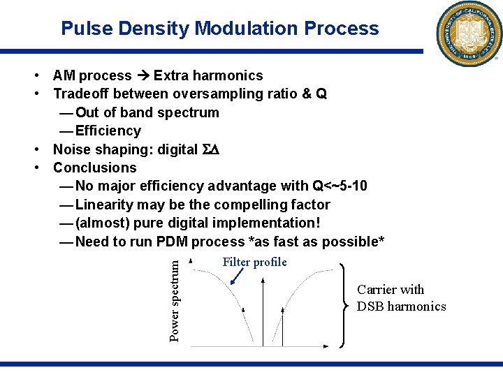
Pulse Density Modulation Process Power spectrum • AM process Extra harmonics • Tradeoff between oversampling ratio & Q — Out of band spectrum — Efficiency • Noise shaping: digital • Conclusions — No major efficiency advantage with Q<~5 -10 — Linearity may be the compelling factor — (almost) pure digital implementation! — Need to run PDM process *as fast as possible* Filter profile Carrier with DSB harmonics

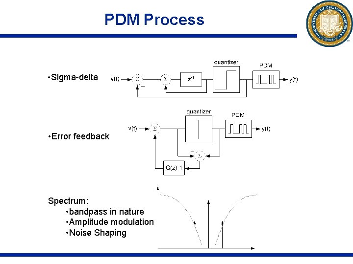
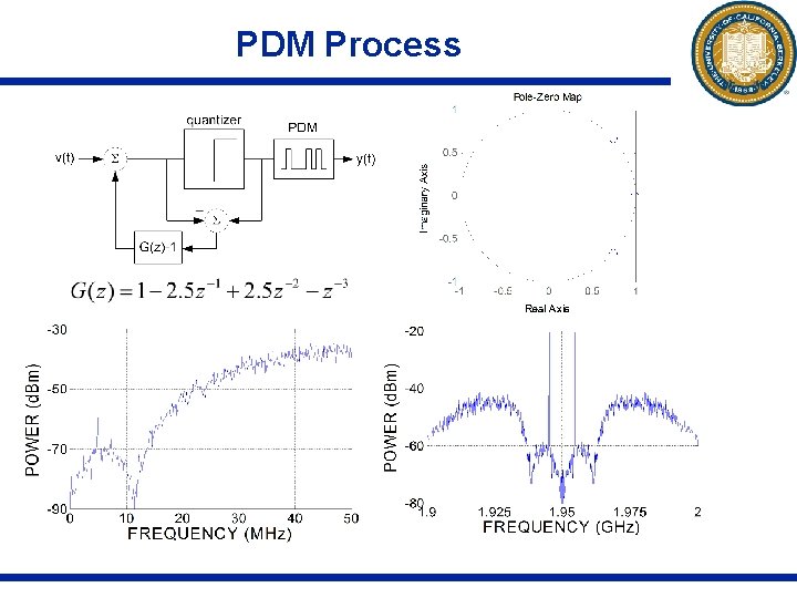
PDM Process • Sigma-delta • Error feedback Spectrum: • bandpass in nature • Amplitude modulation • Noise Shaping

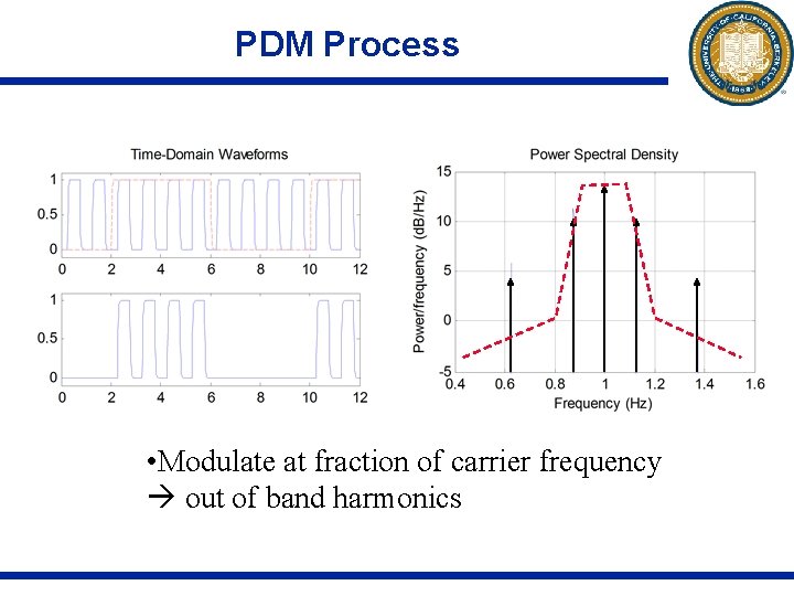
PDM Process • Modulate at fraction of carrier frequency out of band harmonics

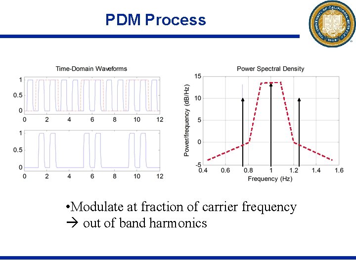
PDM Process • Modulate at fraction of carrier frequency out of band harmonics

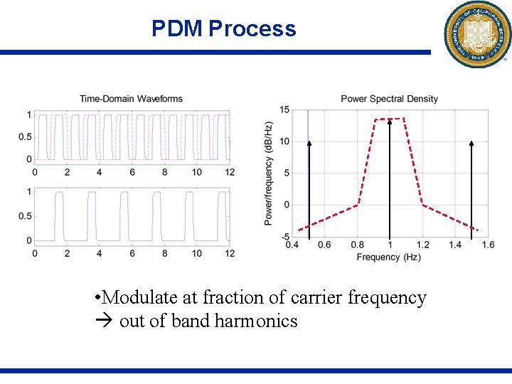
PDM Process • Modulate at fraction of carrier frequency out of band harmonics

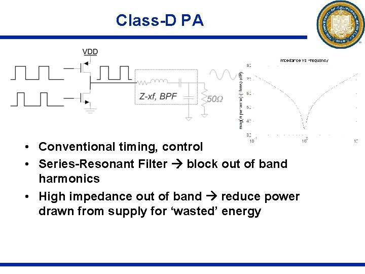
Class-D PA • Conventional timing, control • Series-Resonant Filter block out of band harmonics • High impedance out of band reduce power drawn from supply for ‘wasted’ energy

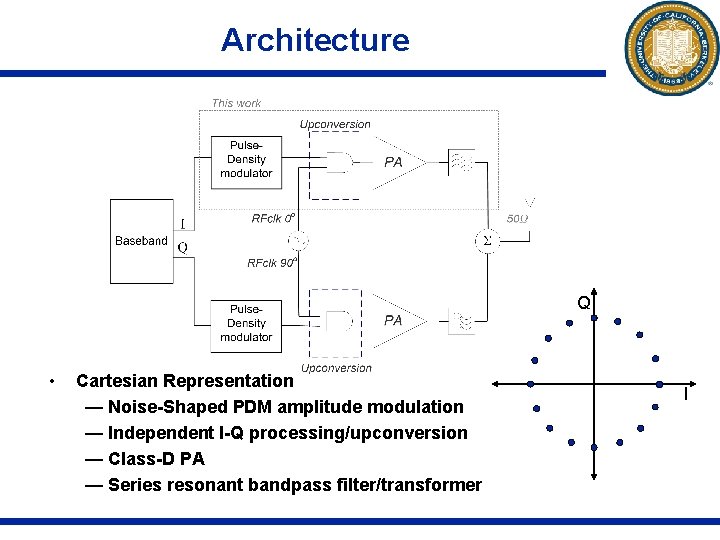
Architecture Q • Cartesian Representation — Noise-Shaped PDM amplitude modulation — Independent I-Q processing/upconversion — Class-D PA — Series resonant bandpass filter/transformer I

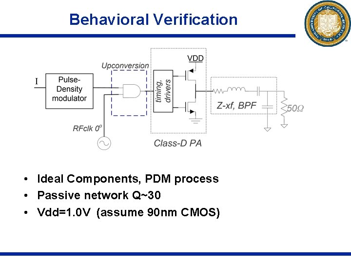
Behavioral Verification • Ideal Components, PDM process • Passive network Q~30 • Vdd=1. 0 V (assume 90 nm CMOS)

Ideal no losses in switches, passives

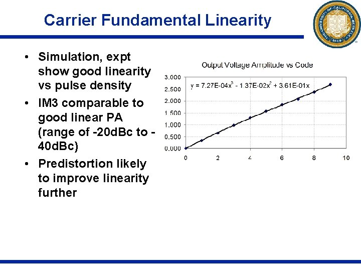
Carrier Fundamental Linearity • Simulation, expt show good linearity vs pulse density • IM 3 comparable to good linear PA (range of -20 d. Bc to 40 d. Bc) • Predistortion likely to improve linearity further

Class. D PA, 90 nm CMOS, Spectre Sim, Q~15 in passives

2 -tone test

Conclusions • Efficiency stays high in power backoff • Future analysis: comparison of series resonant to parallel resonant output filters for class-D PAs • High linearity, compelling argument for this architecture

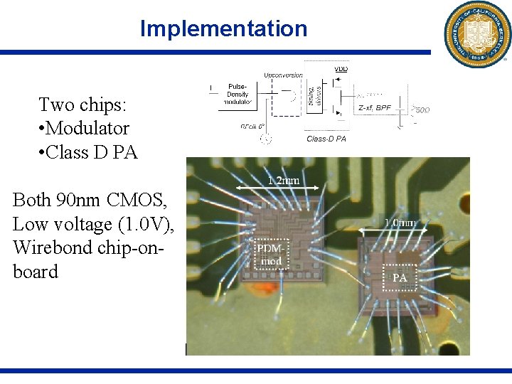
Implementation Two chips: • Modulator • Class D PA Both 90 nm CMOS, Low voltage (1. 0 V), Wirebond chip-onboard

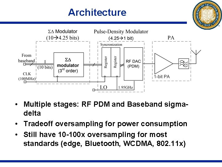
Architecture • Multiple stages: RF PDM and Baseband sigmadelta • Tradeoff oversampling for power consumption • Still have 10 -100 x oversampling for most standards (edge, Bluetooth, WCDMA, 802. 11 x)

PDM Process

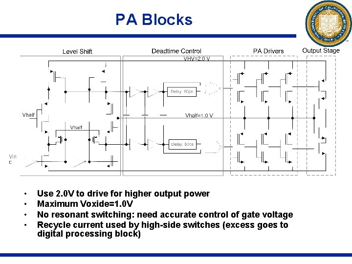
PA Blocks • • Use 2. 0 V to drive for higher output power Maximum Voxide=1. 0 V No resonant switching: need accurate control of gate voltage Recycle current used by high-side switches (excess goes to digital processing block)

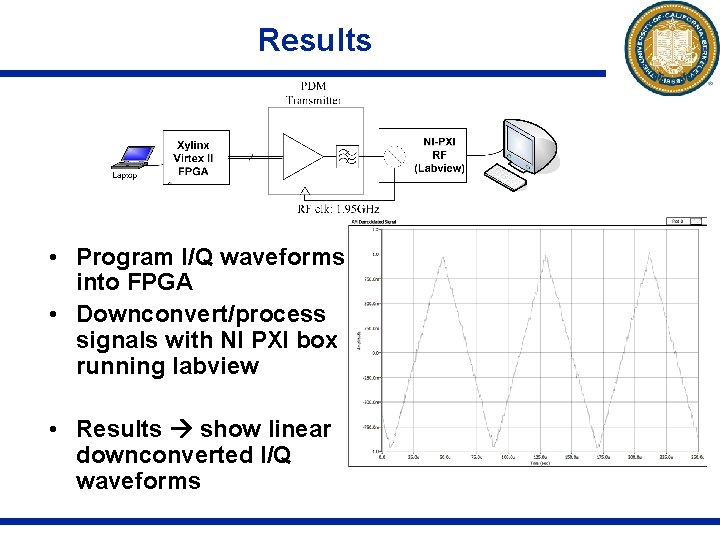
Results • Program I/Q waveforms into FPGA • Downconvert/process signals with NI PXI box running labview • Results show linear downconverted I/Q waveforms

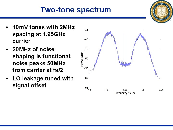
Two-tone spectrum • 10 m. V tones with 2 MHz spacing at 1. 95 GHz carrier • 20 MHz of noise shaping is functional, noise peaks 50 MHz from carrier at fs/2 • LO leakage tuned with signal offset

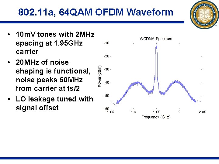
802. 11 a, 64 QAM OFDM Waveform • 10 m. V tones with 2 MHz spacing at 1. 95 GHz carrier • 20 MHz of noise shaping is functional, noise peaks 50 MHz from carrier at fs/2 • LO leakage tuned with signal offset
![References 1 A Jerng and C G Sodini A Wideband DeltaSigma References • • • [1] A. Jerng and C. G. Sodini, "A Wideband Delta-Sigma](https://slidetodoc.com/presentation_image/4ce9a8e411d42aae6e45f7f09074f287/image-44.jpg)
References • • • [1] A. Jerng and C. G. Sodini, "A Wideband Delta-Sigma Digital-RF Modulator for High Data Rate Transmitters, " IEEE Journal of Solid State Circuits, vol. 42, pp. 1710 -1722, Aug. 2007. [2] A. Kavousian, D. K. Su, and B. A. Wooley, "A Digitally Modulated Polar CMOS PA with 20 MHz Signal BW, " IEEE International Solid State Circuits Conference (ISSCC) Dig. Tech. Papers, pp. 78 -588, 2007. [3] S. M. Taleie, T. Copani, B. Bakkaloglu, and S. Kiaei, "A bandpass Delta-Sigma RF-DAC with embedded FIR reconstruction filter, " IEEE International Solid State Circuits Conference (ISSCC) Dig. Tech. Papers, pp. 578 -579, 2006. [4] R. B. Staszewski, J. Wallberg, S. Rezeq, C. -M. Hung, O. Eliezer, S. Vemulapalli, C. Fernando, K. Maggio, R. Staszewski, N. Barton, M. -C. Lee, P. Cruise, M. Entezari, K. Muhammad, and D. Leipold, "All-digital PLL and GSM/EDGE transmitter in 90 nm CMOS, " IEEE International Solid State Circuits Conference, vol. 1, pp. 316 -600, Feb. 2005. [5] J. Lindeberg, J. Vanakka, J. Sommarek, and K. Halonen, "A 1. 5 -V direct digital synthesizer with tunable delta-sigma modulator in 0. 12 um CMOS, " IEEE Journal of Solid State Circuits, vol. 40, pp. 1978 -1982, Sept. 2005. [6] F. Wang, D. Kimball, D. Y. Lie, P. Asbeck, and L. E. Larson, "A Monolithic High-Efficiency 2. 4 GHz 20 d. Bm Si. Ge Bi. CMOS Envelope. Tracking OFDM Power Amplifier, " IEEE Journal of Solid State Circuits, vol. 42, pp. 1271 -1281, June 2007.