EMT 182 ANALOG ELECTRONICS 1 Power Amplifiers POWER

- Slides: 47

EMT 182 ANALOG ELECTRONICS 1 Power Amplifiers

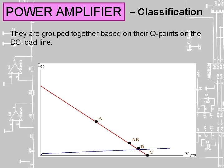
POWER AMPLIFIER – Classification They are grouped together based on their Q-points on the DC load line.

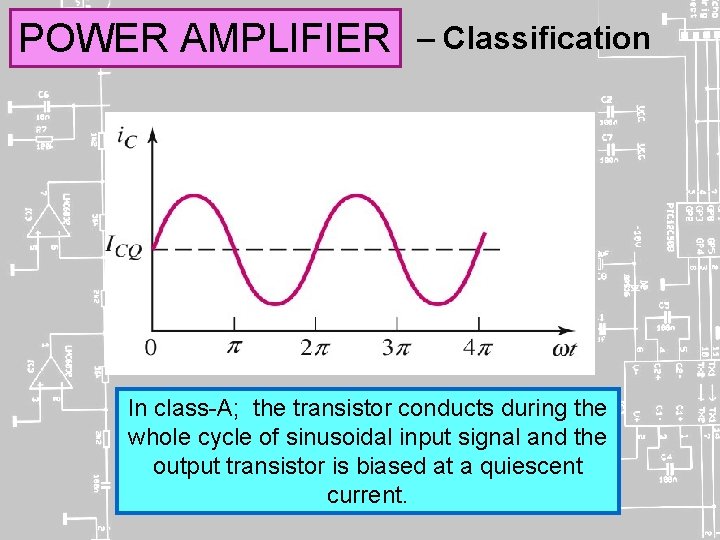
POWER AMPLIFIER – Classification In class-A; the transistor conducts during the whole cycle of sinusoidal input signal and the output transistor is biased at a quiescent current.

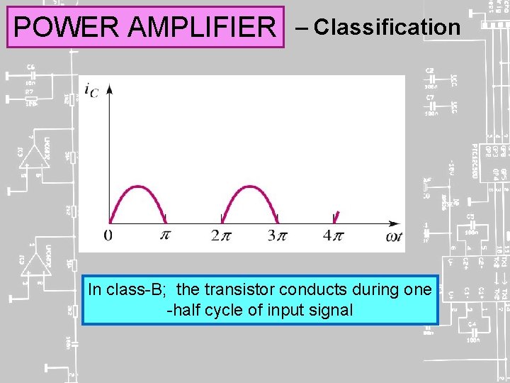
POWER AMPLIFIER – Classification In class-B; the transistor conducts during one -half cycle of input signal

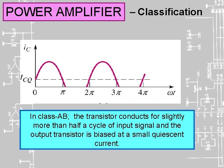
POWER AMPLIFIER – Classification In class-AB; the transistor conducts for slightly more than half a cycle of input signal and the output transistor is biased at a small quiescent current.

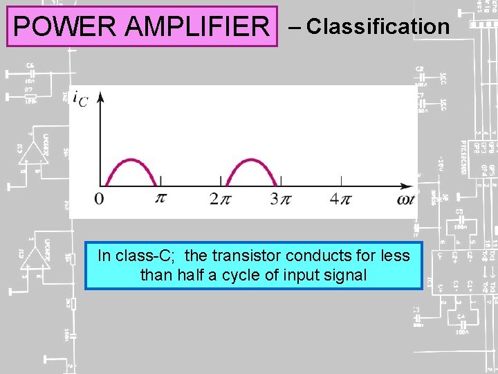
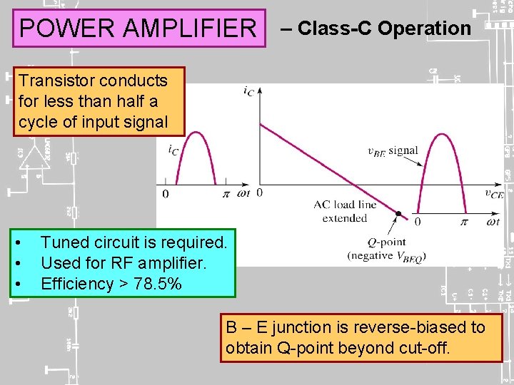
POWER AMPLIFIER – Classification In class-C; the transistor conducts for less than half a cycle of input signal

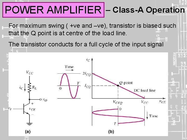
POWER AMPLIFIER – Class-A Operation For maximum swing ( +ve and –ve), transistor is biased such that the Q point is at centre of the load line. The transistor conducts for a full cycle of the input signal

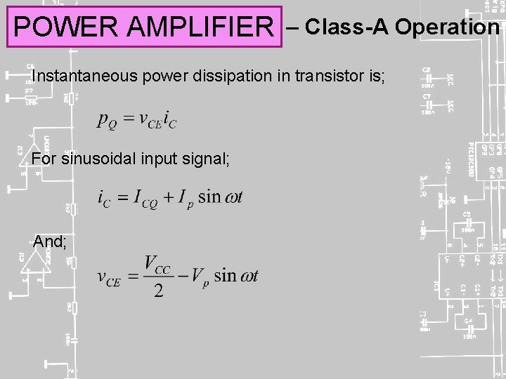
POWER AMPLIFIER – Class-A Operation Instantaneous power dissipation in transistor is; For sinusoidal input signal; And;

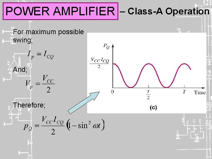
POWER AMPLIFIER For maximum possible swing; And; Therefore; – Class-A Operation

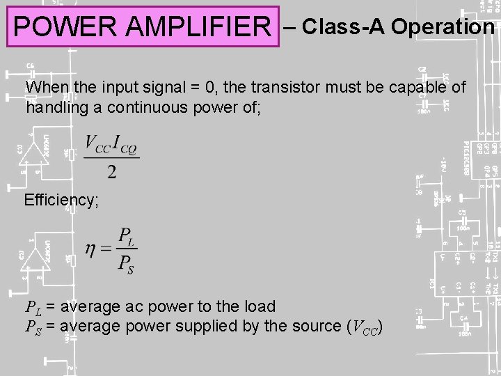
POWER AMPLIFIER – Class-A Operation When the input signal = 0, the transistor must be capable of handling a continuous power of; Efficiency; PL = average ac power to the load PS = average power supplied by the source (VCC)

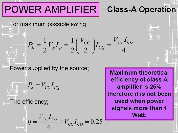
POWER AMPLIFIER – Class-A Operation For maximum possible swing; Power supplied by the source; The efficiency; Maximum theoretical efficiency of class A amplifier is 25% therefore it is not been used when power signals more than 1 Watt.

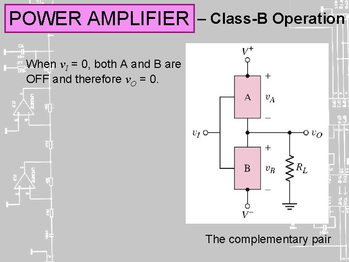
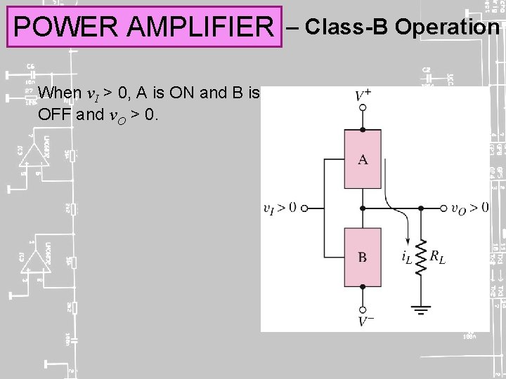
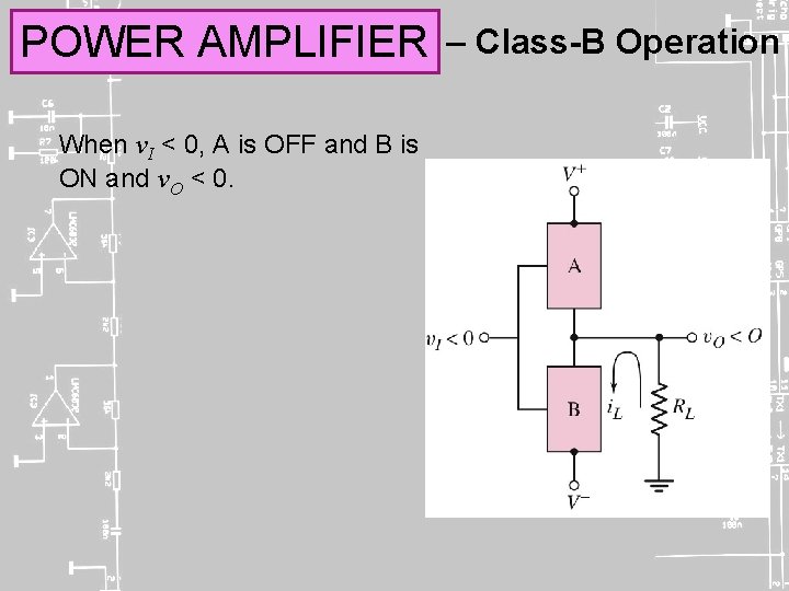
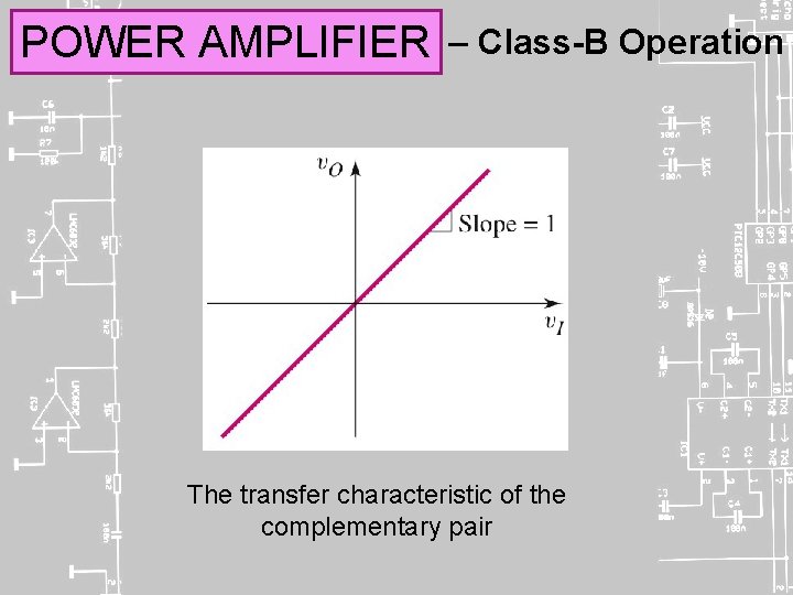
POWER AMPLIFIER – Class-B Operation Consists of complementary pair electronic devices One conducts for one half cycle of the input signal and the other conducts for another half of the input signal Both devices are off when the input is zero (See Figure)

POWER AMPLIFIER – Class-B Operation When v. I = 0, both A and B are OFF and therefore v. O = 0. The complementary pair

POWER AMPLIFIER When v. I > 0, A is ON and B is OFF and v. O > 0. – Class-B Operation

POWER AMPLIFIER When v. I < 0, A is OFF and B is ON and v. O < 0. – Class-B Operation

POWER AMPLIFIER – Class-B Operation The transfer characteristic of the complementary pair

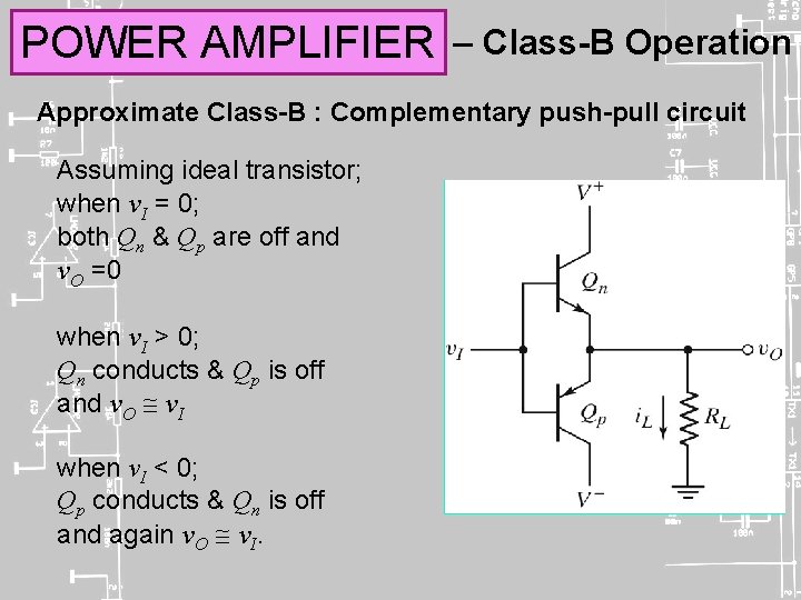
POWER AMPLIFIER – Class-B Operation Approximate Class-B : Complementary push-pull circuit Assuming ideal transistor; when v. I = 0; both Qn & Qp are off and v. O =0 when v. I > 0; Qn conducts & Qp is off and v. O v. I when v. I < 0; Qp conducts & Qn is off and again v. O v. I.

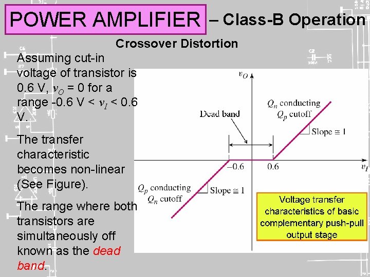
POWER AMPLIFIER – Class-B Operation Crossover Distortion Assuming cut-in voltage of transistor is 0. 6 V, v. O = 0 for a range -0. 6 V < v. I < 0. 6 V. The transfer characteristic becomes non-linear (See Figure). The range where both transistors are simultaneously off known as the dead band.

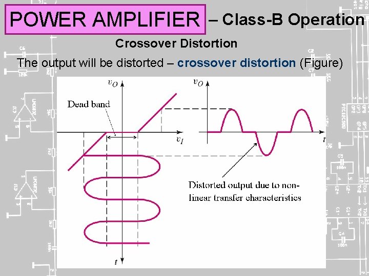
POWER AMPLIFIER – Class-B Operation Crossover Distortion The output will be distorted – crossover distortion (Figure)

POWER AMPLIFIER – Class-B Operation Crossover Distortion Crossover distortion can be eliminated by biasing the transistor with small quiescent current when vi = 0 V

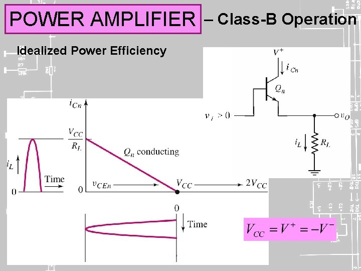
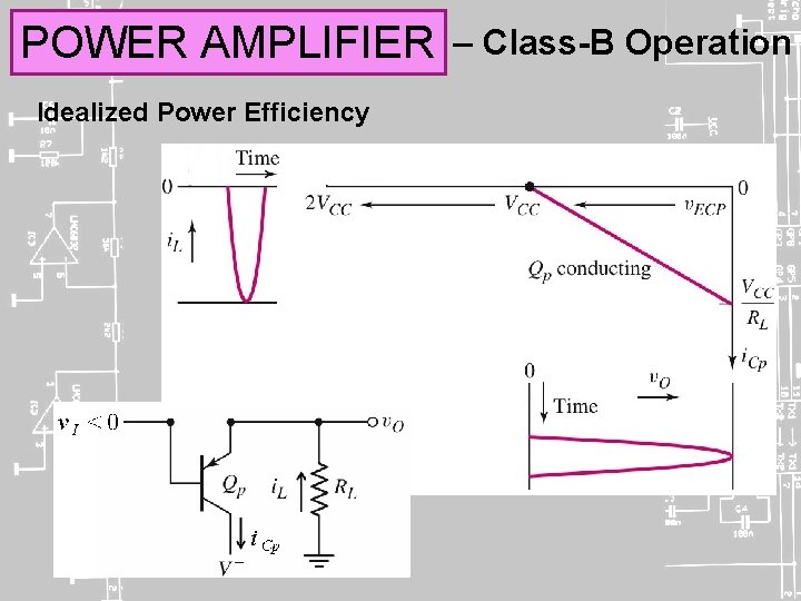
POWER AMPLIFIER Idealized Power Efficiency – Class-B Operation

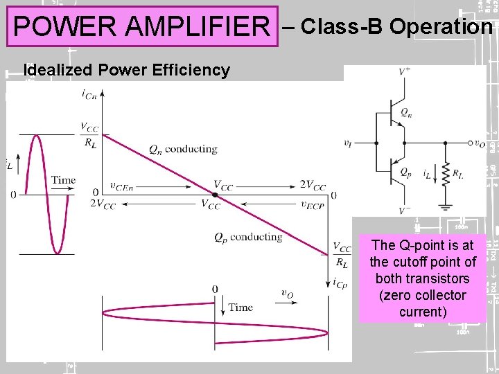
POWER AMPLIFIER Idealized Power Efficiency – Class-B Operation

POWER AMPLIFIER – Class-B Operation Idealized Power Efficiency The Q-point is at the cutoff point of both transistors (zero collector current)

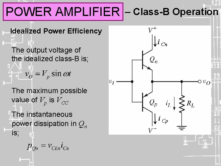
POWER AMPLIFIER Idealized Power Efficiency The output voltage of the idealized class-B is; The maximum possible value of Vp is VCC The instantaneous power dissipation in Qn is; – Class-B Operation

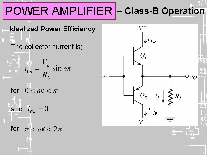
POWER AMPLIFIER Idealized Power Efficiency The collector current is; for and for – Class-B Operation

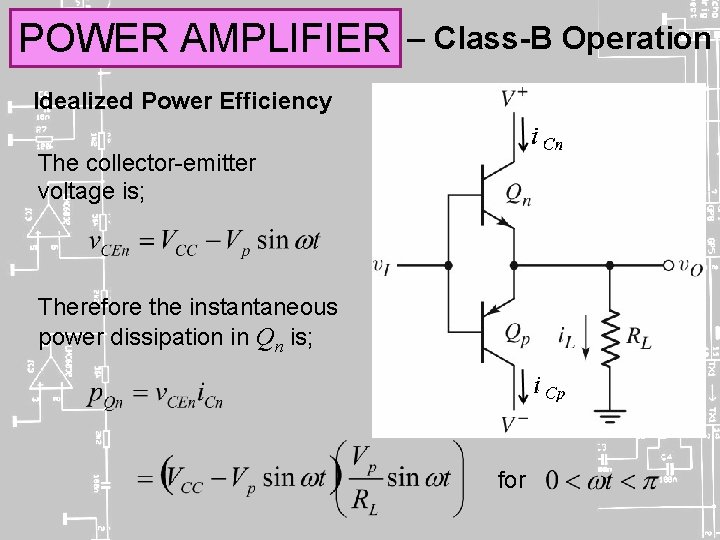
POWER AMPLIFIER – Class-B Operation Idealized Power Efficiency The collector-emitter voltage is; Therefore the instantaneous power dissipation in Qn is; for

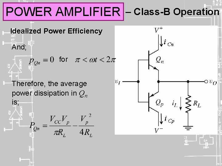
POWER AMPLIFIER Idealized Power Efficiency And; for Therefore, the average power dissipation in Qn is; – Class-B Operation

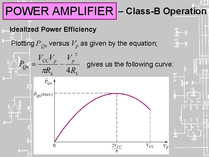
POWER AMPLIFIER – Class-B Operation Idealized Power Efficiency Plotting PQn versus Vp as given by the equation; gives us the following curve:

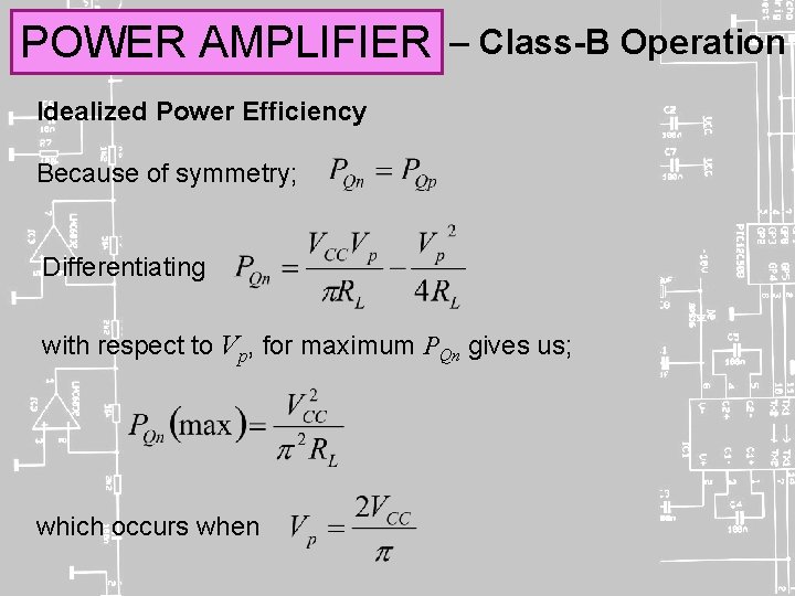
POWER AMPLIFIER – Class-B Operation Idealized Power Efficiency Because of symmetry; Differentiating with respect to Vp, for maximum PQn gives us; which occurs when

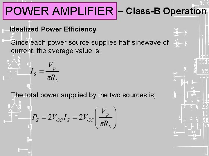
POWER AMPLIFIER – Class-B Operation Idealized Power Efficiency Since each power source supplies half sinewave of current, the average value is; The total power supplied by the two sources is;

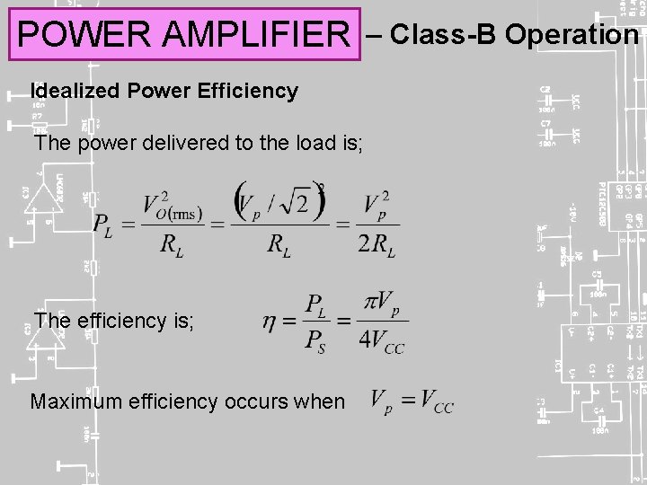
POWER AMPLIFIER Idealized Power Efficiency The power delivered to the load is; The efficiency is; Maximum efficiency occurs when – Class-B Operation

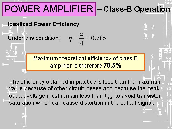
POWER AMPLIFIER – Class-B Operation Idealized Power Efficiency Under this condition; Maximum theoretical efficiency of class B amplifier is therefore 78. 5% The efficiency obtained in practice is less than the maximum value because of other circuit losses and because the peak output voltage must remain less than VCC to avoid transistor saturation which can cause distortion in the output signal.

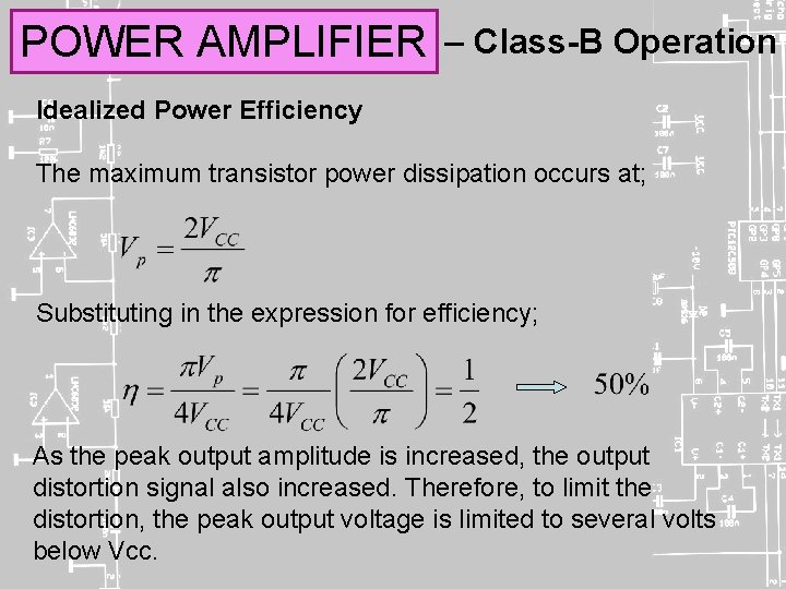
POWER AMPLIFIER – Class-B Operation Idealized Power Efficiency The maximum transistor power dissipation occurs at; Substituting in the expression for efficiency; As the peak output amplitude is increased, the output distortion signal also increased. Therefore, to limit the distortion, the peak output voltage is limited to several volts below Vcc.

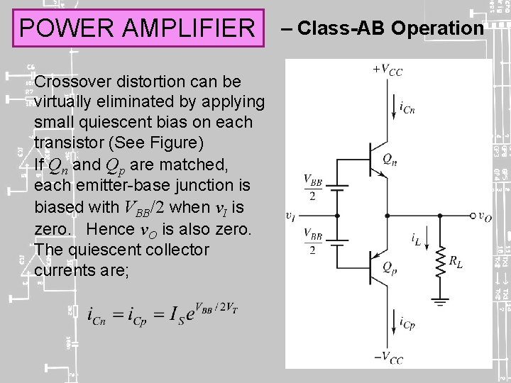
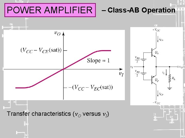
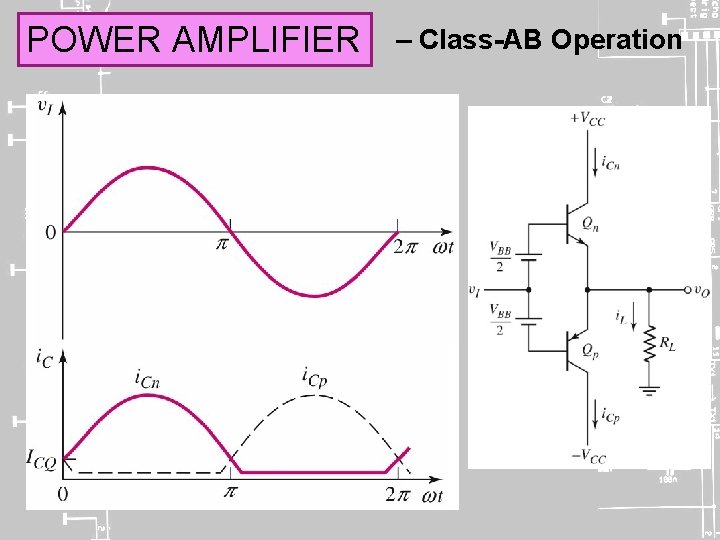
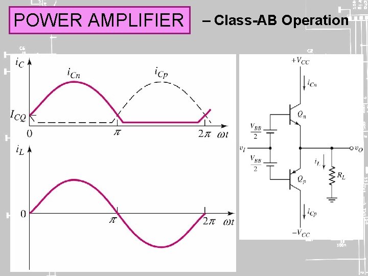
POWER AMPLIFIER Crossover distortion can be virtually eliminated by applying small quiescent bias on each transistor (See Figure) If Qn and Qp are matched, each emitter-base junction is biased with VBB/2 when v. I is zero. Hence v. O is also zero. The quiescent collector currents are; – Class-AB Operation

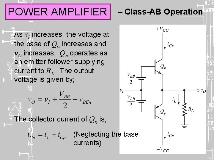
POWER AMPLIFIER – Class-AB Operation As v. I increases, the voltage at the base of Qn increases and v. O increases. Qn operates as an emitter follower supplying current to RL. The output voltage is given by; The collector current of Qn is; (Neglecting the base currents)

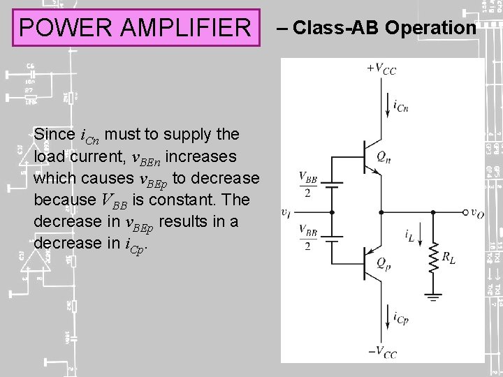
POWER AMPLIFIER Since i. Cn must to supply the load current, v. BEn increases which causes v. BEp to decrease because VBB is constant. The decrease in v. BEp results in a decrease in i. Cp. – Class-AB Operation

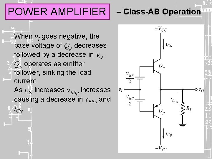
POWER AMPLIFIER When v. I goes negative, the base voltage of Qp decreases followed by a decrease in v. O. Qp operates as emitter follower, sinking the load current. As i. Cp increases v. EBp increases causing a decrease in v. BEn and i. Cn. – Class-AB Operation

POWER AMPLIFIER – Class-AB Operation Transfer characteristics (v. O versus v. I)

POWER AMPLIFIER – Class-AB Operation

POWER AMPLIFIER – Class-AB Operation

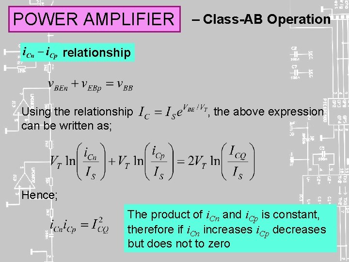
POWER AMPLIFIER – Class-AB Operation relationship Using the relationship can be written as; , the above expression Hence; The product of i. Cn and i. Cp is constant, therefore if i. Cn increases i. Cp decreases but does not to zero

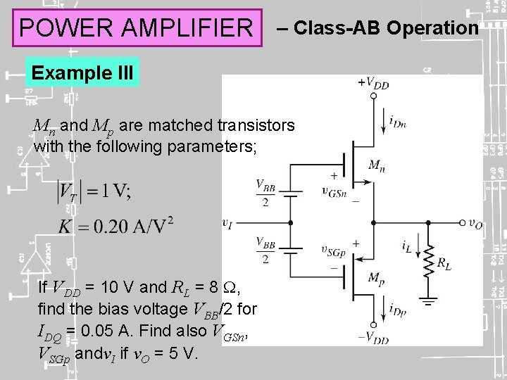
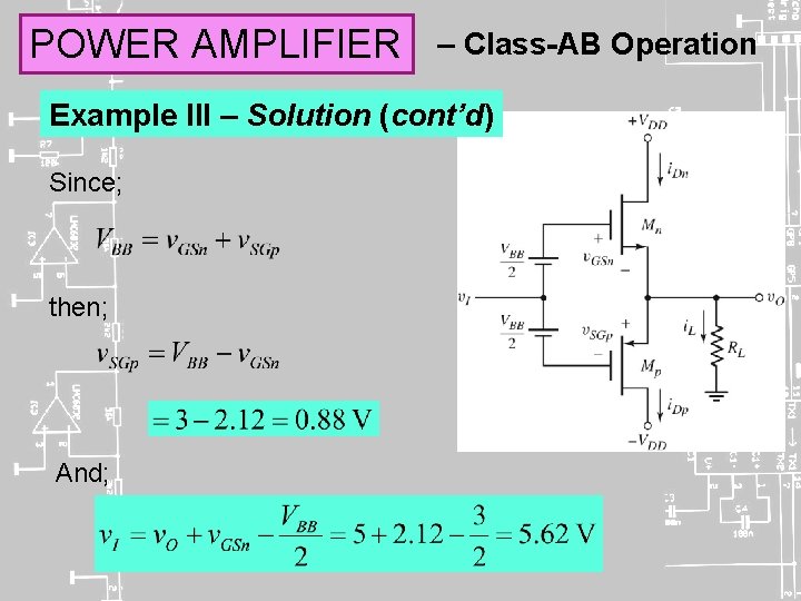
POWER AMPLIFIER – Class-AB Operation Example III Mn and Mp are matched transistors with the following parameters; If VDD = 10 V and RL = 8 , find the bias voltage VBB/2 for IDQ = 0. 05 A. Find also VGSn, VSGp andv. I if v. O = 5 V.

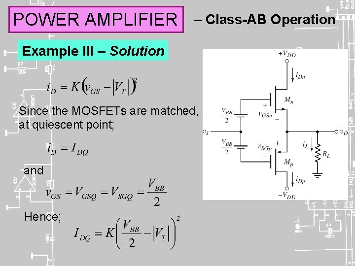
POWER AMPLIFIER – Class-AB Operation Example III – Solution Since the MOSFETs are matched, at quiescent point; and Hence;

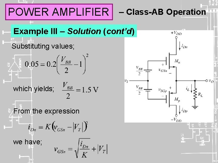
POWER AMPLIFIER – Class-AB Operation Example III – Solution (cont’d) Substituting values; which yields; From the expression we have;

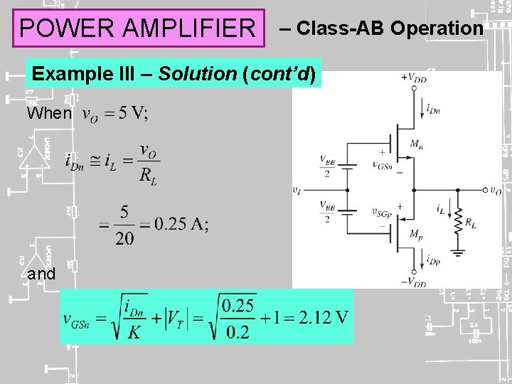
POWER AMPLIFIER – Class-AB Operation Example III – Solution (cont’d) When and

POWER AMPLIFIER – Class-AB Operation Example III – Solution (cont’d) Since; then; And;

POWER AMPLIFIER – Class-C Operation Transistor conducts for less than half a cycle of input signal • • • Tuned circuit is required. Used for RF amplifier. Efficiency > 78. 5% B – E junction is reverse-biased to obtain Q-point beyond cut-off.