Analog Electronics Update on ICECAL 3 and delay
- Slides: 13
Analog Electronics Update on ICECAL 3 and delay unit J. Mauricio, E. Picatoste Universitat de Barcelona Institut de Ciències del Cosmos ICC-UB Calorimeter Upgrade Meeting – October 16 th 2013
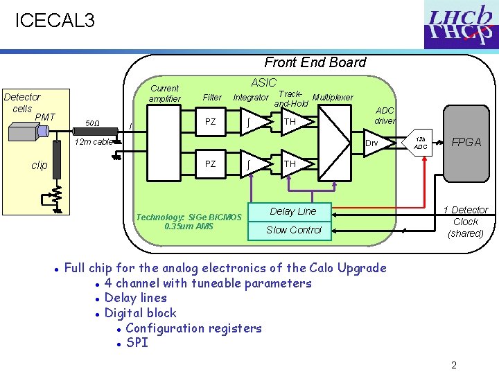
ICECAL 3 Front End Board Detector cells PMT Current amplifier 50Ω I ASIC Filter Integrator PZ ʃ Track- Multiplexer and-Hold TH 12 m cable clip Drv PZ Technology: Si. Ge Bi. CMOS 0. 35 um AMS ADC driver ʃ 12 b ADC FPGA TH Delay Line Slow Control 1 Detector Clock (shared) Full chip for the analog electronics of the Calo Upgrade 4 channel with tuneable parameters Delay lines Digital block Configuration registers SPI 2
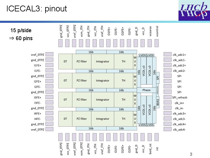
ICECAL 3: pinout 15 p/side ⇒ 60 pins 3
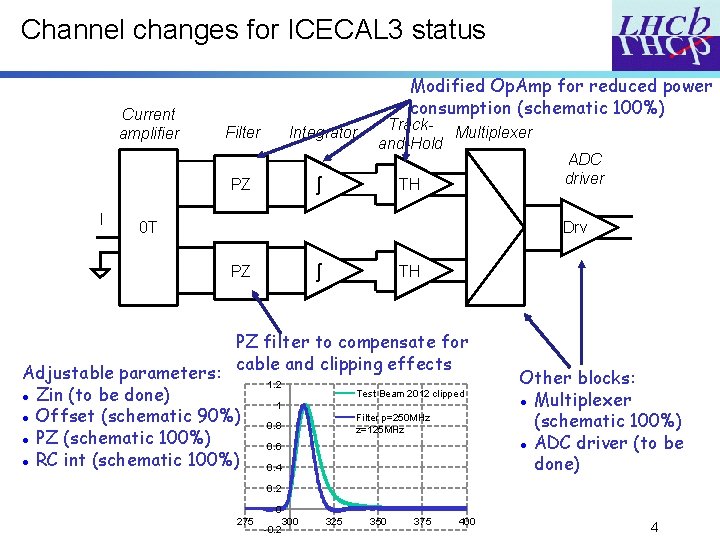
Channel changes for ICECAL 3 status Current amplifier Modified Op. Amp for reduced power consumption (schematic 100%) Filter Integrator ʃ PZ I Track. Multiplexer and-Hold TH 0 T ADC driver Drv ʃ PZ TH PZ filter to compensate for cable and clipping effects Adjustable parameters: Zin (to be done) Offset (schematic 90%) PZ (schematic 100%) RC int (schematic 100%) 1. 2 Test Beam 2012 clipped 1 Filter p=250 MHz z=125 MHz 0. 8 0. 6 0. 4 Other blocks: Multiplexer (schematic 100%) ADC driver (to be done) 0. 2 0 275 -0. 2 300 325 350 375 400 4
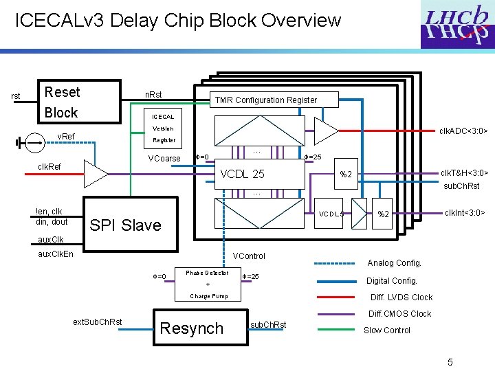
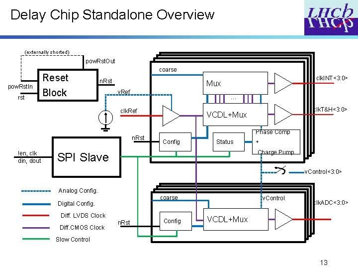
ICECALv 3 Delay Chip Block Overview rst Reset n. Rst Block TMR Configuration Register ICECAL Version v. Ref clk. ADC<3: 0> Register VCoarse clk. Ref ··· Φ=0 VCDL 25 Φ=25 clk. T&H<3: 0> %2 sub. Ch. Rst ··· !en, clk din, dout VCDL 5 SPI Slave %2 clk. Int<3: 0> aux. Clk. En VControl Φ=0 Phase Detector Φ=25 + Charge Pump ext. Sub. Ch. Rst Analog Config. Digital Config. Diff. LVDS Clock Diff. CMOS Clock Resynch sub. Ch. Rst Slow Control 5
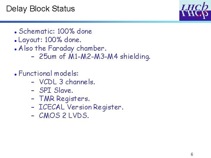
Delay Block Status Schematic: 100% done Layout: 100% done. Also the Faraday chamber. – 25 um of M 1 -M 2 -M 3 -M 4 shielding. Functional models: – VCDL 3 channels. – SPI Slave. – TMR Registers. – ICECAL Version Register. – CMOS 2 LVDS. 6
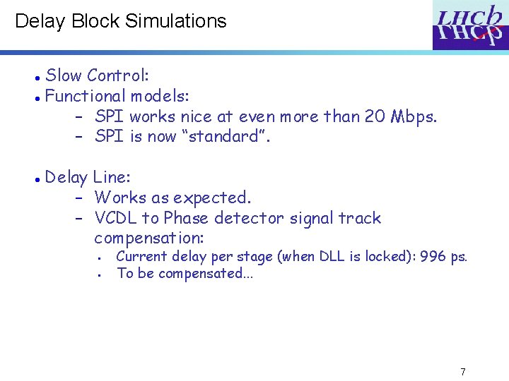
Delay Block Simulations Slow Control: Functional models: – SPI works nice at even more than 20 Mbps. – SPI is now “standard”. Delay Line: – Works as expected. – VCDL to Phase detector signal track compensation: § § Current delay per stage (when DLL is locked): 996 ps. To be compensated. . . 7
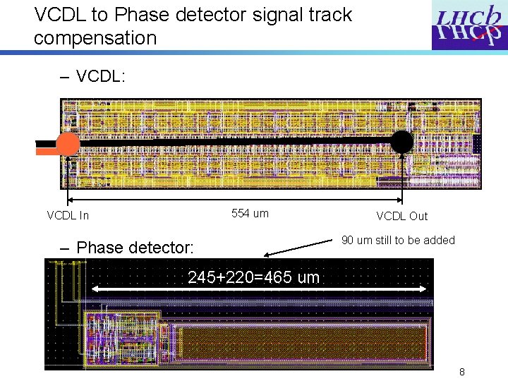
VCDL to Phase detector signal track compensation – VCDL: To PD. . . 554 um VCDL In – Phase detector: VCDL Out 90 um still to be added 245+220=465 um 8
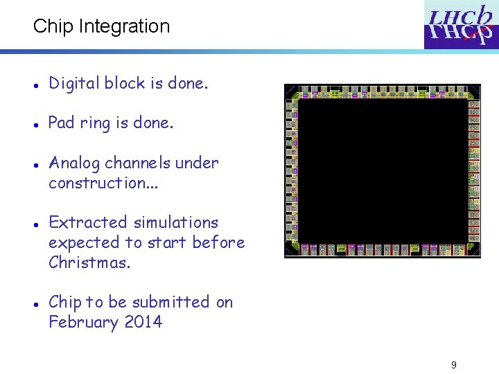
Chip Integration Digital block is done. Pad ring is done. Analog channels under construction. . . Extracted simulations expected to start before Christmas. Chip to be submitted on February 2014 9
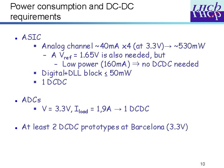
Power consumption and DC-DC requirements ASIC § Analog channel ~40 m. A x 4 (at 3. 3 V)→ ~530 m. W – A Vref = 1. 65 V is also needed, but – Low power (160 m. A) ⇒ no DCDC needed § Digital+DLL block ≤ 50 m. W § 1 DCDC ADCs § V = 3. 3 V, Iload = 1, 9 A → 1 DCDC At least 2 DCDC prototypes at Barcelona (3. 3 V) 10
Backup 11
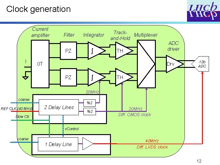
Clock generation Current amplifier Filter PZ I Integrator ʃ Track. Multiplexer and-Hold TH 0 T ADC driver Drv PZ ʃ 12 b ADC TH 20 MHz coarse REF CLK (40 MHz) 2 Delay Lines Slow Ctl. %2 %2 20 MHz Diff. CMOS clock v. Control coarse 1 Delay Line 40 MHz Diff. LVDS clock 12
Delay Chip Standalone Overview (externally shorted) pow. Rst. Out pow. Rst. In rst Reset coarse n. Rst Block v. Ref ··· clk. Ref n. Rst !en, clk din, dout clk. INT<3: 0> Mux clk. T&H<3: 0> VCDL+Mux Phase Comp Config Status + Charge Pump SPI Slave v. Control<3: 0> Analog Config. coarse Digital Config. Diff. LVDS Clock Diff. CMOS Clock n. Rst Config v. Control clk. ADC<3: 0> VCDL+Mux Slow Control 13