Digital Design A Systems Approach Lecture 12 Timing
- Slides: 25

Digital Design: A Systems Approach Lecture 12: Timing (c) 2005 -2012 W. J. Dally 1

Readings • • L 12: Chapter 15 L 13: Chapter 27 & 28 (c) 2005 -2012 W. J. Dally 2

Timing • How fast can a system run? • Will it work at any speed? (c) 2005 -2012 W. J. Dally 3

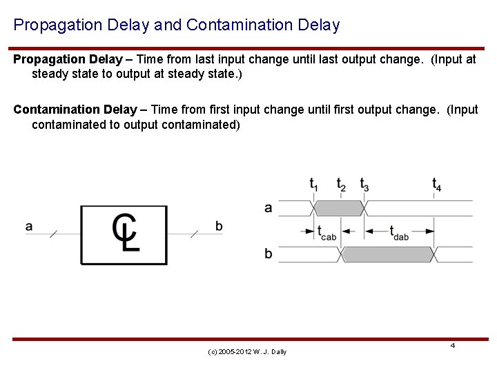
Propagation Delay and Contamination Delay Propagation Delay – Time from last input change until last output change. (Input at steady state to output at steady state. ) Contamination Delay – Time from first input change until first output change. (Input contaminated to output contaminated) (c) 2005 -2012 W. J. Dally 4

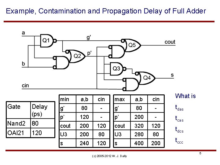
Example, Contamination and Propagation Delay of Full Adder min a, b cin Delay (ps) g’ 80 p’ Nand 2 80 OAI 21 120 Gate What is max a, b cin - g’ 80 - tdas 120 - p’ 200 - tcas cout 200 120 cout 320 120 U 3 200 80 U 3 280 80 s 240 120 s 400 200 (c) 2005 -2012 W. J. Dally tdcs tccc 5

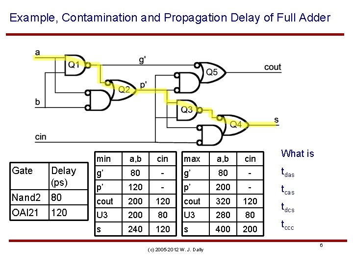
Example, Contamination and Propagation Delay of Full Adder min a, b cin Delay (ps) g’ 80 p’ Nand 2 80 OAI 21 120 Gate What is max a, b cin - g’ 80 - tdas 120 - p’ 200 - tcas cout 200 120 cout 320 120 U 3 200 80 U 3 280 80 s 240 120 s 400 200 (c) 2005 -2012 W. J. Dally tdcs tccc 6

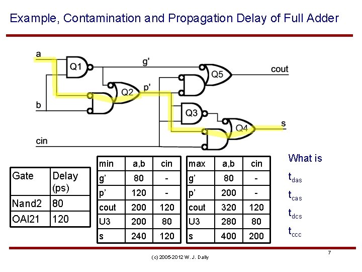
Example, Contamination and Propagation Delay of Full Adder min a, b cin Delay (ps) g’ 80 p’ Nand 2 80 OAI 21 120 Gate What is max a, b cin - g’ 80 - tdas 120 - p’ 200 - tcas cout 200 120 cout 320 120 U 3 200 80 U 3 280 80 s 240 120 s 400 200 (c) 2005 -2012 W. J. Dally tdcs tccc 7

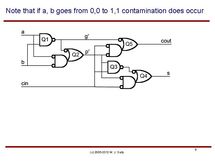
Note that if a, b goes from 0, 0 to 1, 1 contamination does occur (c) 2005 -2012 W. J. Dally 8

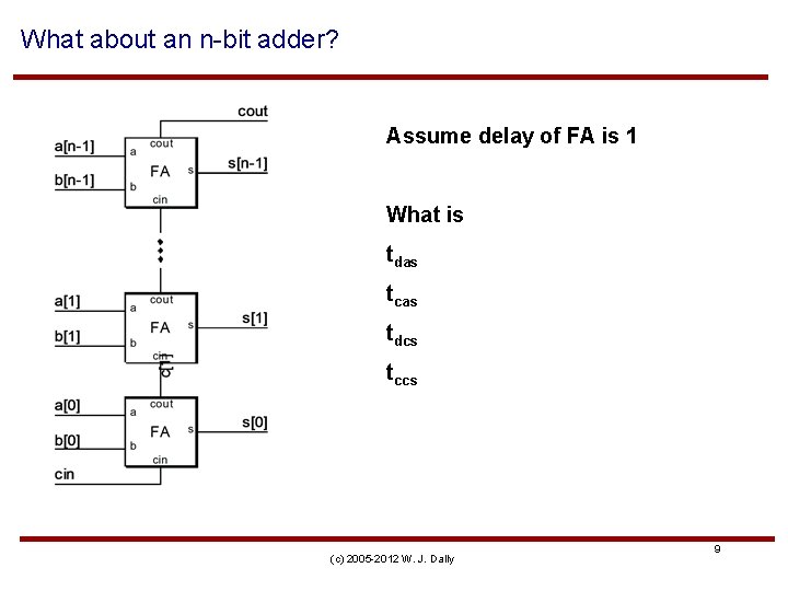
What about an n-bit adder? Assume delay of FA is 1 What is tdas tcas tdcs tccs (c) 2005 -2012 W. J. Dally 9

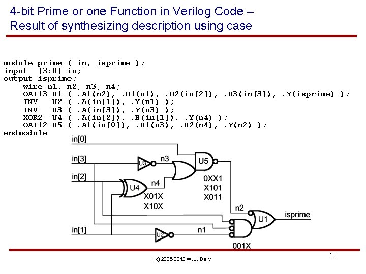
4 -bit Prime or one Function in Verilog Code – Result of synthesizing description using case module prime ( in, isprime ); input [3: 0] in; output isprime; wire n 1, n 2, n 3, n 4; OAI 13 U 1 (. A 1(n 2), . B 1(n 1), . B 2(in[2]), . B 3(in[3]), . Y(isprime) ); INV U 2 (. A(in[1]), . Y(n 1) ); INV U 3 (. A(in[3]), . Y(n 3) ); XOR 2 U 4 (. A(in[2]), . B(in[1]), . Y(n 4) ); OAI 12 U 5 (. A 1(in[0]), . B 1(n 3), . B 2(n 4), . Y(n 2) ); endmodule (c) 2005 -2012 W. J. Dally 10

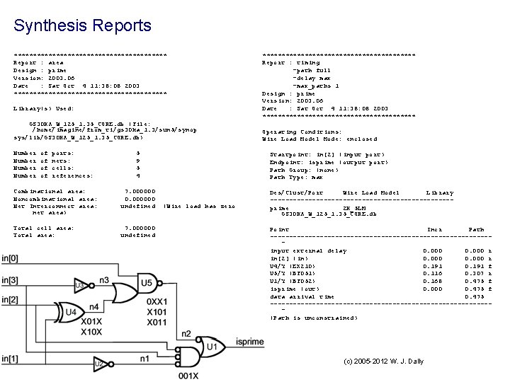
Synthesis Reports ******************** Report : area Design : prime Version: 2003. 06 Date : Sat Oct 4 11: 38: 08 2003 ******************** Library(s) Used: GS 30 KA_W_125_1. 35_CORE. db (File: /home/imagine/from_ti/gs 30 ka_1. 3/sun 5/synop sys/lib/GS 30 KA_W_125_1. 35_CORE. db) Number of of ports: nets: cells: references: 5 9 5 4 Combinational area: Noncombinational area: Net Interconnect area: net area) 7. 000000 0. 000000 undefined Total cell area: Total area: 7. 000000 undefined ******************** Report : timing -path full -delay max -max_paths 1 Design : prime Version: 2003. 06 Date : Sat Oct 4 11: 38: 08 2003 ******************** Operating Conditions: Wire Load Model Mode: enclosed Startpoint: in[2] (input port) Endpoint: isprime (output port) Path Group: (none) Path Type: max (Wire load has zero Des/Clust/Port Wire Load Model Library ------------------------prime 2 K_5 LM GS 30 KA_W_125_1. 35_CORE. db Point Incr Path -----------------------------input external delay 0. 000 r in[2] (in) 0. 000 r U 4/Y (EX 210) 0. 191 f U 5/Y (BF 051) 0. 116 0. 307 r U 1/Y (BF 052) 0. 168 0. 475 f isprime (out) 0. 000 0. 475 f data arrival time 0. 475 -----------------------------(Path is unconstrained) (c) 2005 -2012 W. J. Dally

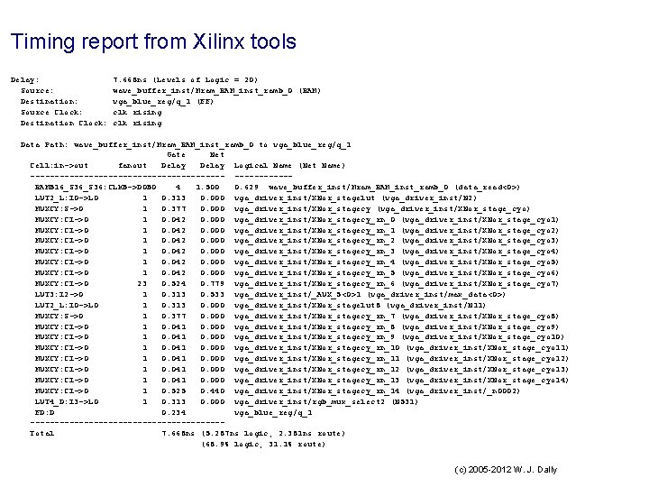
Timing report from Xilinx tools Delay: Source: Destination: Source Clock: Destination Clock: 7. 668 ns (Levels of Logic = 20) wave_buffer_inst/Mram_RAM_inst_ramb_0 (RAM) vga_blue_reg/q_1 (FF) clk rising Data Path: wave_buffer_inst/Mram_RAM_inst_ramb_0 to vga_blue_reg/q_1 Gate Net Cell: in->out fanout Delay Logical Name (Net Name) --------------------RAMB 16_S 36: CLKB->DOB 0 4 1. 500 0. 629 wave_buffer_inst/Mram_RAM_inst_ramb_0 (data_read<0>) LUT 2_L: I 0 ->LO 1 0. 313 0. 000 vga_driver_inst/XNor_stagelut (vga_driver_inst/N 2) MUXCY: S->O 1 0. 377 0. 000 vga_driver_inst/XNor_stagecy (vga_driver_inst/XNor_stage_cyo) MUXCY: CI->O 1 0. 042 0. 000 vga_driver_inst/XNor_stagecy_rn_0 (vga_driver_inst/XNor_stage_cyo 1) MUXCY: CI->O 1 0. 042 0. 000 vga_driver_inst/XNor_stagecy_rn_1 (vga_driver_inst/XNor_stage_cyo 2) MUXCY: CI->O 1 0. 042 0. 000 vga_driver_inst/XNor_stagecy_rn_2 (vga_driver_inst/XNor_stage_cyo 3) MUXCY: CI->O 1 0. 042 0. 000 vga_driver_inst/XNor_stagecy_rn_3 (vga_driver_inst/XNor_stage_cyo 4) MUXCY: CI->O 1 0. 042 0. 000 vga_driver_inst/XNor_stagecy_rn_4 (vga_driver_inst/XNor_stage_cyo 5) MUXCY: CI->O 1 0. 042 0. 000 vga_driver_inst/XNor_stagecy_rn_5 (vga_driver_inst/XNor_stage_cyo 6) MUXCY: CI->O 23 0. 524 0. 779 vga_driver_inst/XNor_stagecy_rn_6 (vga_driver_inst/XNor_stage_cyo 7) LUT 3: I 2 ->O 1 0. 313 0. 533 vga_driver_inst/_AUX_5<0>1 (vga_driver_inst/max_data<0>) LUT 2_L: I 0 ->LO 1 0. 313 0. 000 vga_driver_inst/XNor_stagelut 8 (vga_driver_inst/N 11) MUXCY: S->O 1 0. 377 0. 000 vga_driver_inst/XNor_stagecy_rn_7 (vga_driver_inst/XNor_stage_cyo 8) MUXCY: CI->O 1 0. 041 0. 000 vga_driver_inst/XNor_stagecy_rn_8 (vga_driver_inst/XNor_stage_cyo 9) MUXCY: CI->O 1 0. 041 0. 000 vga_driver_inst/XNor_stagecy_rn_9 (vga_driver_inst/XNor_stage_cyo 10) MUXCY: CI->O 1 0. 041 0. 000 vga_driver_inst/XNor_stagecy_rn_10 (vga_driver_inst/XNor_stage_cyo 11) MUXCY: CI->O 1 0. 041 0. 000 vga_driver_inst/XNor_stagecy_rn_11 (vga_driver_inst/XNor_stage_cyo 12) MUXCY: CI->O 1 0. 041 0. 000 vga_driver_inst/XNor_stagecy_rn_12 (vga_driver_inst/XNor_stage_cyo 13) MUXCY: CI->O 1 0. 041 0. 000 vga_driver_inst/XNor_stagecy_rn_13 (vga_driver_inst/XNor_stage_cyo 14) MUXCY: CI->O 1 0. 525 0. 440 vga_driver_inst/XNor_stagecy_rn_14 (vga_driver_inst/_n 0002) LUT 4_D: I 3 ->LO 1 0. 313 0. 000 vga_driver_inst/rgb_mux_select 2 (N 531) FD: D 0. 234 vga_blue_reg/q_1 --------------------Total 7. 668 ns (5. 287 ns logic, 2. 381 ns route) (68. 9% logic, 31. 1% route) (c) 2005 -2012 W. J. Dally

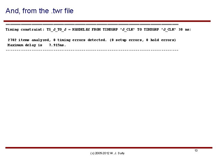
And, from the. twr file ======================================== Timing constraint: TS_J_TO_J = MAXDELAY FROM TIMEGRP "J_CLK" TO TIMEGRP "J_CLK" 30 ns; 2782 items analyzed, 0 timing errors detected. (0 setup errors, 0 hold errors) Maximum delay is 7. 915 ns. ---------------------------------------- (c) 2005 -2012 W. J. Dally 13

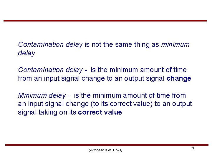
Contamination delay is not the same thing as minimum delay Contamination delay - is the minimum amount of time from an input signal change to an output signal change Minimum delay - is the minimum amount of time from an input signal change (to its correct value) to an output signal taking on its correct value (c) 2005 -2012 W. J. Dally 14

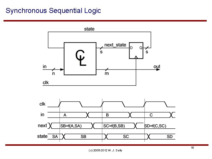
Synchronous Sequential Logic (c) 2005 -2012 W. J. Dally 15

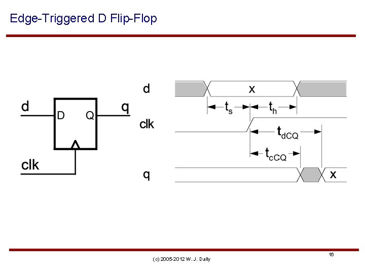
Edge-Triggered D Flip-Flop (c) 2005 -2012 W. J. Dally 16

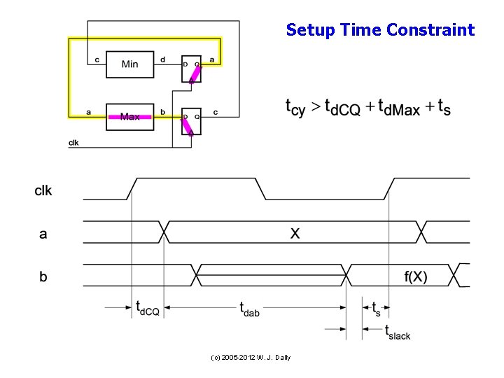
Setup Time Constraint (c) 2005 -2012 W. J. Dally

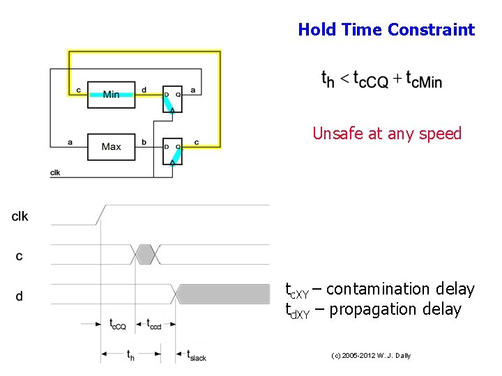
Hold Time Constraint Unsafe at any speed tc. XY – contamination delay td. XY – propagation delay (c) 2005 -2012 W. J. Dally

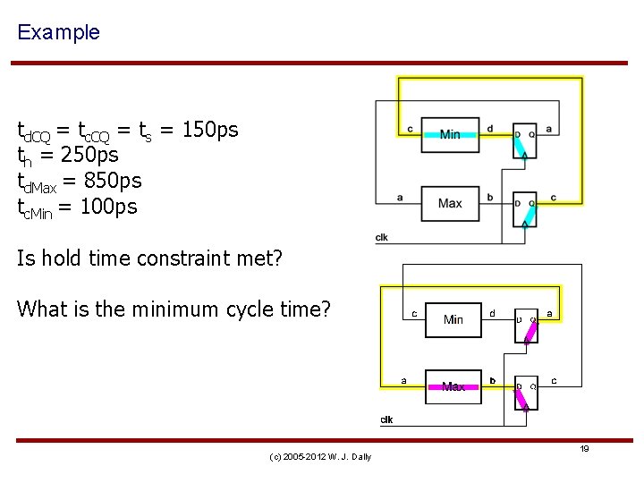
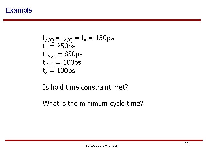
Example td. CQ = tc. CQ = ts = 150 ps th = 250 ps td. Max = 850 ps tc. Min = 100 ps Is hold time constraint met? What is the minimum cycle time? (c) 2005 -2012 W. J. Dally 19

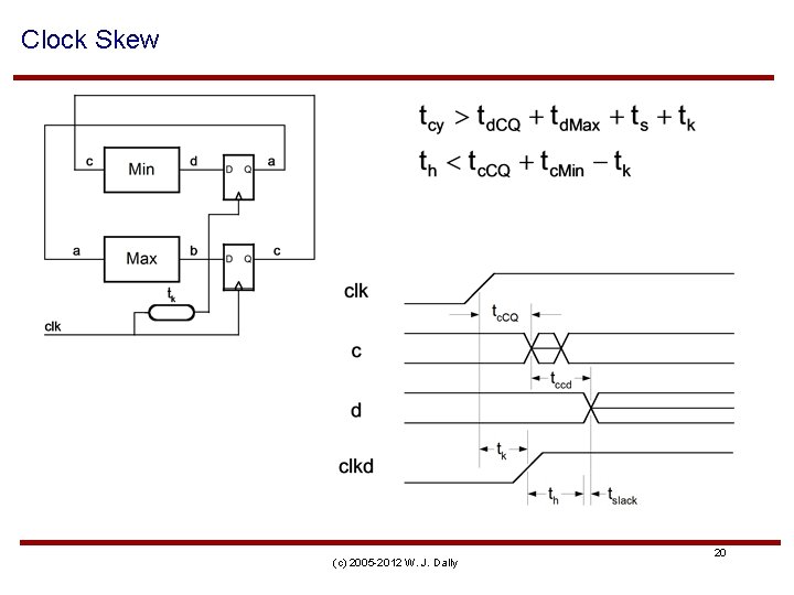
Clock Skew (c) 2005 -2012 W. J. Dally 20

Example td. CQ = tc. CQ = ts = 150 ps th = 250 ps td. Max = 850 ps tc. Min = 100 ps tk = 100 ps Is hold time constraint met? What is the minimum cycle time? (c) 2005 -2012 W. J. Dally 21

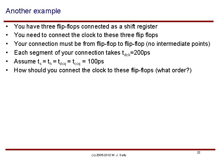
Another example • • • You have three flip-flops connected as a shift register You need to connect the clock to these three flip flops Your connection must be from flip-flop to flip-flop (no intermediate points) Each segment of your connection takes tdck=200 ps Assume ts = th = tdcq = tccq = 100 ps How should you connect the clock to these flip-flops (what order? ) (c) 2005 -2012 W. J. Dally 22

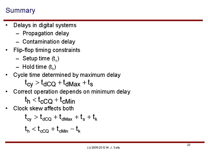
Summary • Delays in digital systems – Propagation delay – Contamination delay • Flip-flop timing constraints – Setup time (ts) – Hold time (th) • Cycle time determined by maximum delay • Correct operation depends on minimum delay • Clock skew affects both (c) 2005 -2012 W. J. Dally 23

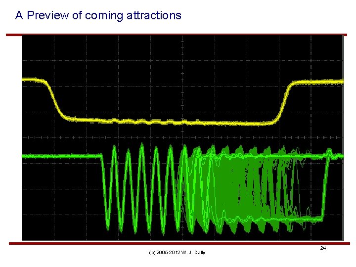
A Preview of coming attractions (c) 2005 -2012 W. J. Dally 24

Coming Next Lecture • Metastability and synchronization failure • or – When good flip-flops go bad (c) 2005 -2012 W. J. Dally 25