EMT 3693 POWER ELECTRONICS Chapter 2 Power semiconductor


")
 based switches Infineon: https: //www. infineon. com/dgdl/Infineon-Presentation_Ga. N_Gallium. Nitride_APEC")
 states i. e. on-state")


 ON (forward-conducting state) under forward biased condition.")


 Standard or")
 General purpose diode • The standard or general-purpose rectifier diodes have relatively high")


 Schottky diode • Schottky diode has metal-to-semiconductor junction rather than a P-N junction.")
 Schottky diode cont … • Often used in low voltage applications where diode")
: Maximum average forward current VRRM: Maximum repetitive peak reverse voltage")


")


")


: Channel on-resistance ID: Drain current")


 applied between the emitter to")

 VCES: Maximum collector-emitter breakdown voltage")

 represents the voltage drop between collector and emitter during on-state,")
 – Bidirectional triode thyristors (triacs) –")
 J 1 J 2 J 3 device structure (Infineon, Bipolar Semiconductors, AN")
 • Methods for turning on a thyristor (SCR): • Method")


 • During the on-state, the anode current (IA) is limited")
 (Agrawal, Newnes, 2001, pp. 116)")
 I-V characteristics IL – latching current Ih – holding current VBF –")
 forward conduction reverse blocking forward blocking (Daniel W. Hart, 2010)")
 like the SCR can be turned")
: on-state RMS current VDRM: Maximum peak repetitive forward blocking voltage VRRM: Maximum peak")


 based switches Infineon: https: //www. infineon. com/dgdl/Infineon-Presentation_Ga. N_Gallium. Nitride_APEC 2016 -APv 01_00")
 “Silicon carbide (Si. C) has a wide bandgap of 3")
 Infineon, The Future of Power Semiconductors, 2016")
 • “Ga. N has an even higher bandgap (3. 4")
 and")

- Slides: 58
EMT 369/3 POWER ELECTRONICS Chapter 2 Power semiconductor devices
Power semiconductor switches • In power electronic circuits, power semiconductor devices are used as switches. The switches are turned on and off periodically. • Examples of power semiconductor switches includes 1) Power diodes (turn on and turn off are uncontrollable) 2) Power transistors (turn on and turn off are controllable) a) Power MOSFETS b) Power bipolar junction transistors (BJTs) c) Insulated bipolar junction transistor (IGBT) 3) Thyristors (SCR) (semi-controllable)
Evolution of Power Semiconductor Switches Thyristor family (Bimal K. Bose, 2006)
Today’s switch technology Silicon (Si) based switches Infineon: https: //www. infineon. com/dgdl/Infineon-Presentation_Ga. N_Gallium. Nitride_APEC 2016 -APv 01_00 -EN. pdf? file. Id=5546 d 46253 a 864 fe 0153 d 0 a 8 f 85132 c 5
Ideal electronic switches • An electronic switch has TWO (2) states i. e. on-state and offstate. • Ideally, the switch is a short circuit during the on-state and an open circuit during the offstate. • In this case, either the switch voltage or switch current is zero, making the power absorbed by it is zero. Is Vs ON OFF
Practical aspects of power semiconductor switches • In practical case, these power switches absorb some power when in the on-state (conduction loss) and when making transitions between the on-state and off-state (switching loss), causing some power dissipation and affecting the circuit efficiency. (Daniel W. Hart, 2010 ) • Power semiconductor devices like power diodes, power MOSFETS and power BJTs have higher power, voltage and current handling capability than the ordinary small signal diodes.
Power loss in switches IGBT Technical training for FSC family: https: //slideplayer. com/slide/6192776/
Power diodes • A diode is a) ON (forward-conducting state) under forward biased condition. The anode is more positive than the cathode. b) OFF (reverse-blocking state) under reverse biased condition. The anode is more negative than the cathode. anode cathode • The turn on and turn off of a diode are uncontrollable in that the on and off conditions are determined by current and voltages in the circuit. (Daniel W. Hart, 2010)
Power diode I-V characteristics VF • A practical diode has reverse leakage current and forward voltage drop VF. • Forward voltage drop and forward current give rise to conduction loss during the on-state.
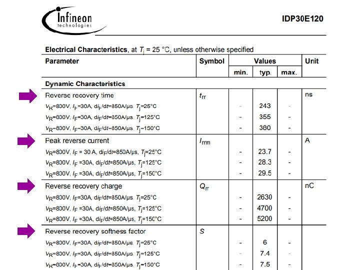
• diode - Reverse recovery When switching from the conducting to the blocking state, i. e. on-state to off-state, a diode has stored charge that must first be discharged before the diode blocks reverse current. This discharge takes a finite amount of time known as reverse recovery time, or trr. The current in the diode decreases and momentarily becomes negative (flowing in the reverse direction) before becoming zero, as shown in the figure below. This phenomena may be important for high frequency applications. (Maxim Integrated, Glossary term) • (Maxim Integrated, Glossary term) (Daniel W. Hart, 2010, pp. 7) • Qrr Some important terms IRM – peak reverse recovery current trr – reverse recovery time Qrr – reverse recovery charge (area under I vs t graph) IF – forward current d. IF/dt – rate of falling IF
Types of power diodes • Power diodes can be classified into: 1) Standard or general purpose diodes 2) Fast recovery diodes 3) Schottky diodes (Muhammad H. Rashid, Prentice Hall, pp. 386)
(a) General purpose diode • The standard or general-purpose rectifier diodes have relatively high reverse recovery time, typically 25 s; and are used in low-speed applications, where recovery time is not critical. (b) Fast-recovery diode • Fast recovery diodes have short reverse recovery time (trr), normally less than 5 s. • The fast-recovery diodes are essential for high-frequency switching of power converters. (Muhammad H. Rashid, Prentice Hall, pp. 386)
Example: Fast recovery diode VRRM: Repetitive peak reverse voltage IF: Continuous forward current VF: Forward voltage drop
IDP 30 E 120
(c) Schottky diode • Schottky diode has metal-to-semiconductor junction rather than a P-N junction. • Schottky diode has a lower forward voltage drop compared to that of a P-N junction. • Schottky diode, a unipolar device, has extremely small charge storage time. Schottky diode is, therefore, not subjected to recovery transients / has small recovery transients and turn on and turn off faster than a P-N junction diode. • Schottky diode has higher reverse leakage current and smaller breakdown voltage compared to those of a P-N junction. (Daniel W. Hart, 2010 & (S. M. Sze & Kwok K. Ng, Wiley, 3 ed. , 2007, pp. 154) )
(c) Schottky diode cont … • Often used in low voltage applications where diode drops are significant relative to other circuit voltages. • Reverse voltage is limited to about 200 V. (Daniel W. Hart, 2010)
Example: Schottky diode IF(AV): Maximum average forward current VRRM: Maximum repetitive peak reverse voltage VF: Forward voltage drop
Unipolar and bipolar devices • A unipolar device uses only one carrier type (either electrons or holes) to conduct current through the device. • A bipolar device uses both carrier types i. e. both electrons and holes to conduct current through the device. http: //ece-classnotes. blogspot. com/2016/02/why-is-fet-known-as-unipolar-device. html https: //uk. farnell. com/unipolar-transistor-definition
Power transistors • Unlike the diode, the turn on and turn off of transistors are controllable. • THREE (3) types of power transistors which will be considered are: a) Bipolar Junction Transistor (BJT) b) Metal Field Oxide Semiconductor Field Effect Transistor (MOSFET) c) Insulated Gate Bipolar Transistor (IGBT)
N-P-N BJT device structure Lightly doped drift region Vertical cross section of N-P-N BJT device structure • • For power transistors, vertical structure is preferred because it maximizes the cross sectional area through which the on-state current flows. In this case, current flows in vertical direction. Thus, both on-state resistance and power loss are minimized. (NPTEL, Power Electronics, L-3)
N-P-N BJT (Daniel W. Hart, 2010)
N-P-N BJT detailed I-V characteristics On-State region Active region “On-State” region is sometimes known as “saturation” region.
Turn on/off BJT • To operate a power BJT as a switch, the power BJT must be operated in the on-state region (saturation region) during turn on and cutoff region during turn off. • To turn on a power BJT as a switch, current must be injected into the base (B) to drive the BJT into saturation. A high base current is required to turn on the transistor and is still needed to keep the transistor in saturation. (Daniel W. Hart, 2010 & Infineon, IGBT or MOSFET: Choose wisely) (Daniel W. Hart, 2010 & Toshiba, MOSFET Gate Drive Circuit, 2018) • Zero base current results in cutoff. (Daniel W. Hart, 2010 ) • on-state conduction loss is governed by the on-state collector -emitter saturation voltage v. CE(sat). Power loss = v. CE(sat) i. C. (Infineon, IGBT or MOSFET: Choose wisely)
N-channel power MOSFET The alternating n+ n- p n+ structure embeds a parasitic BJT (with its base and source region emitter shorted by the source metallization) into each body region MOSFET cell. With an effective short circuit drift region between the body and the body diode source, the BJT always remain in cut off and its collector-base junction is represented as an anti parallel diode (called the body diode) in the circuit symbol of a Power MOSFET. Formation of inversion layer Vertical cross section of N-channel power MOSFET cell (NPTEL, Power Electronics, L-6)
P-channel and N-channel power MOSFET • • A body diode is formed between the source and drain regions. The body diode can be an advantage in power electronic circuits like inverters for driving inductive loads.
N-channel power MOSFET body diode (Daniel W. Hart, 2010)
N-channel power MOSFET On-State region Active region “On-State” region is sometimes known as “ohmic” region / “linear” region on-state channel resistance RDS(ON) Cutoff region In on-state region, drain current (i. D) is almost proportional to the drainsource voltage (VDS). In ACTIVE region, drain current (i. D) becomes almost independent of V and determined by the gate-source voltage (V ).
Turn on/off power MOSFET • To operate a power MOSFET as a switch, the power MOSFET must be operated in the on-state region (ohmic region / linear region) during turn on and cutoff region during turn off. • To turn on a n-channel power MOSFET as a switch, v. GS – vth< v. DS. • To turn off a n-channel power MOSFET, v. GS < vth. • During on-state, v. DS = i. D RDS(on) • on-state conduction loss is due to on-state channel resistance RDS(on). Power loss = RDS(on) i. D. • The oxide layer beneath the gate results in high input impedance gate. Once the MOSFET transistors are turned-on, their drive current is practically zero. (Texas Instruments, Fundamentals of MOSFET and IGBT Gate Driver Circuits , SLUA 618 A – March 2017)
Power MOSFET example VDSS: Drain-to-source breakdown voltage RDS(on): Channel on-resistance ID: Drain current
Power MOSFET example
IGBT - Introduction • A MOSFET is a unipolar device, which has less minority carrier storage delay, thus giving the advantage of switching speed over BJT which is a bipolar device and tend to have long switching times. A BJT has relatively slow turn-off characteristics (known as the current tail). (Daniel W. Hart, 2010, pp. 11) (Daniel W. Hart, 2010 & Infineon, IGBT or MOSFET: Choose wisely) • A MOSFET has high gate input impedance which makes the gate easy to be driven/controlled. Once the MOSFET is turned on, the drive current is practically zero, resulting in low driving power. In contrast, a BJT generally requires a high base current to turn on and a base current is still needed to keep the device in saturation even if the device has been turned on. (Texas Instruments, Fundamentals of MOSFET and IGBT Gate Driver Circuits , SLUA 618 A – March 2017) (Daniel W. Hart, 2010 & Infineon, IGBT or MOSFET: Choose wisely) (Daniel W. Hart, 2010 & Toshiba, MOSFET Gate Drive Circuit, 2018)
IGBT - Introduction • A BJT has a low common-emitter saturation voltage, which minimizes the on-state power loss, and has high current handling capability, which both are necessary in high power handling devices. (Toshiba, IGBTs, Application note) (Infineon, IGBT or MOSFET: Choose wisely ) • An Insulated Gate Bipolar Transistor (IGBT) combines characteristics of high gate input impedance and high switching speed of a MOSFET and low saturation voltage and high current handling capability of a BJT. (Toshiba, IGBTs, Application note) (Infineon, IGBT or MOSFET: Choose wisely ) • The drive circuit for the IGBT is like that of the MOSFET, while the on-state characteristics (conduction characteristics) are like those of the BJT. (Daniel W. Hart, 2010, pp. 11)
N-channel IGBT device structure body region Path of electron flow drift region injecting layer Vertical cross section of N-channel IGBT cell • An N-channel IGBT is basically an N-channel power MOSFET constructed on a p-type substrate (P+ injecting layer). • Consequently, operation of an IGBT is very similar to that of a power MOSFET. (Diagram is adapted based on International Rectifier: IGBT or MOSFET: Choose wisely & NPTEL, Power Electronics, L-7)
N-channel IGBT device operation • A positive voltage (VGE) applied between the emitter to gate terminals causes electrons to be drawn toward the gate terminal in the body region. • If the gate-emitter voltage (VGE) is at or above the gate-emitter threshold voltage (VGE(th)), a conducting channel is formed across the body region. • This conducting channel shorts the N+ emitter layer and the N- drain drift layer and electrons flow from emitter to collector. • This flow of electrons draws holes from the P+ substrate into the N- drift region and move towards the emitter. Basically, current is injected into the base of the P-N-P transistor formed by the body region (P+), drift region (N-), and (P+) region. (NPTEL, Power Electronics, L-7)
N-channel IGBT device structure ic Schematic of vertical N-channel IGBT structure Equivalent circuit Note that there is a n+ layer between the n- drift region and the p+ injecting layer. This layer which arises from another different generation of IGBT is not included in Slide 35. (Infineon TRENCHSTOP™ 5 S 5 Application note. ) Circuit symbol (a) (NPTEL, Power Electronics, L-7); (b) Infineon AN 983
N-channel IGBT I-V characteristics v. GE < v. GE(th) VCES: Maximum collector-emitter breakdown voltage (NPTEL, Power Electronics, L-7)
IGBT example
IGBT example The VCE(SAT) represents the voltage drop between collector and emitter during on-state, when a nominal current Ic is flowing through the IGBT at a given VGE. (Infineon, Explanation of discrete IGBTs' datasheets, 2018) This leads to on-state conduction loss.
Thyristors • Thyristors include – Silicon-controlled rectifier (SCR) – Bidirectional triode thyristors (triacs) – Gate turnoff thyristor (GTO) • In this class, we shall only focus on SCR that is the first type of thyristor.
Thyristor (SCR) J 1 J 2 J 3 device structure (Infineon, Bipolar Semiconductors, AN 2012 -01) (All. About. Circuits, The Basics of Power Semiconductor Devices: Structures, Symbols, and Operations )
Turn on thyristor (SCR) • Methods for turning on a thyristor (SCR): • Method A (High forward voltage triggering) – Gate circuit is opened i. e. no voltage is applied between the gate and cathode. – A voltage v. AK is applied across the anode and cathode of the SCR. In this case, v. AK is greater than v. BF , which is the forward breakdown voltage of the thyristor, so that junction J 2 of the device will breakdown and the device conducts. – Such method is destructive and should be avoided. • Method B (Gate triggering) – Thyristor is forward biased such that v. AK < v. BF. – Injecting a gate current (Ig) and the anode current (IA) > holding current (Ih). This will be explained in the next slide. – Such method is preferred. (Muhammad H. Rashid, Prentice Hall, pp. 469 - 470)
Method B – gate triggering • This, in turn, causes the PNP J 1 • J 2 NPN J 3 • • A trigger signal is applied between the gate (G) and cathode (K) terminals. • • This causes the NPN equivalent transistor to conduct. • • The collector of the conducting NPN transistor pulls low and thus, the PNP base voltage is pulled to low. equivalent transistor to conduct The collector of the conducting PNP pulls high and thus, the NPN base voltage is pulled to high. This positive feedback (regeneration) reinforces the NPN’s already in the conducting state. The NPN will conduct even in the absence of a gate signal. Once an SCR conducts, it continues for as long as a positive anode voltage is present.
Method B – gate triggering • In short, by applying a small voltage between gate and cathode, the lower NPN transistor will be forced on by the resulting base current, which will cause the upper PNP transistor to conduct, which then supplies the lower NPN transistor’s base with current so that it no longer needs to be activated by a gate voltage. PNP J 1 J 2 NPN J 3
Turn on thyristor (SCR) • During the on-state, the anode current (IA) is limited by the external impedance of the circuit. • The anode current (IA) must be more than the latching current (IL) to ensure that the device is latched into conducting state or in the on-state even after the gate signal is removed (Ig = 0). • Once the SCR conducts, it will remain in the on-state and there is no control over the device. • The device will become unlatched or ONLY turn off when the anode current (IA) drops below the holding current (Ih). • A SCR can be switched off via external circuits which maintain the anode current below the holding current for some time. Such method is known as forced commutation. (Muhammad H. Rashid, Prentice Hall, pp. 469 - 470)
Turn off thyristor (SCR) (Agrawal, Newnes, 2001, pp. 116)
Thyristor (SCR) I-V characteristics IL – latching current Ih – holding current VBF – forward breakdown voltage Ig – gate current VBR – reverse breakdown voltage IL avalanche breakdown SCR has blocking capability in both forward and reverse directions (S. M. Sze & Kwok K. Ng, Wiley, 3 ed. , 2007, pp. 551)
Thyristor (SCR) forward conduction reverse blocking forward blocking (Daniel W. Hart, 2010)
Thyristors cont … • Gate turnoff thyristor (GTO) like the SCR can be turned on by a short duration gate current if the anode-to-cathode voltage is positive. However, unlike the SCR, the GTO can be turned off with a negative gate current. • Bidirectional triode thyristors (triacs) is capable of conducting current in either direction and functionally equivalent to two antiparallel SCRs. (Daniel W. Hart, 2010)
IT(RMS): on-state RMS current VDRM: Maximum peak repetitive forward blocking voltage VRRM: Maximum peak repetitive reverse blocking voltage I : Triggering gate current
BTW 69 -1200 N VTM: Maximum on-state voltage drop IDRM: Maximum forward leakage current at the specified VDRM IRRM: Maximum reverse leakage current at the specified VRRM
Future scenario of power semiconductor switches
Silicon (Si) based switches Infineon: https: //www. infineon. com/dgdl/Infineon-Presentation_Ga. N_Gallium. Nitride_APEC 2016 -APv 01_00 -EN. pdf? file. Id=5546 d 46253 a 864 fe 0153 d 0 a 8 f 85132 c 5
Silicon carbide (Si. C) “Silicon carbide (Si. C) has a wide bandgap of 3 electronvolt (e. V) and a much higher thermal conductivity compared to silicon. Si. C based MOSFETs are most suited for high breakdown, high power applications that operate at high frequency. Compared to silicon, the device parameters such as for example the RDS(on) change less with temperature. This allows designers to work within tighter margins in their designs, allowing extra performance to be delivered. ” https: //www. infineon. com/cms/en/product/power/wide-band-gap-semiconductors-sic-gan/
Silicon carbide (Si. C) Infineon, The Future of Power Semiconductors, 2016
Gallium nitride (Ga. N) • “Ga. N has an even higher bandgap (3. 4 electronvolt) and substantially higher electron mobility than Si. C. Compared to silicon (Si), the breakdown field is ten times higher and the electron mobility is double. Both the output charge and gate charge are ten times lower than with Si, and the reverse recovery charge is almost zero which is key for high frequency operations. ” https: //www. infineon. com/cms/en/product/power/wide-band-gap-semiconductors-sic-gan/
Today’s mainstream technology: Si based power switches Future technology: Silicon Carbide (Si. C) and Gallium Nitride (Ga. N) wide bandgap semiconductor material based power switches Infineon Si. C products: a) Schottky diodes b) MOSFET Infineon, How Ga. N-on-Si can help deliver higher efficiencies in power conversion and power management, 2018
Thank you