Calorimeter Upgrade Analog Electronics D Gascon J Mauricio

- Slides: 39

Calorimeter Upgrade: Analog Electronics D. Gascon, J. Mauricio, E. Picatoste ICCUB//Si. UB, University of Barcelona

2 Outline I. Calorimeter upgrade: analog electronics II. System design III. Digital building blocks IV. Tests V. Production 28 February 2021 Calo FE PRR

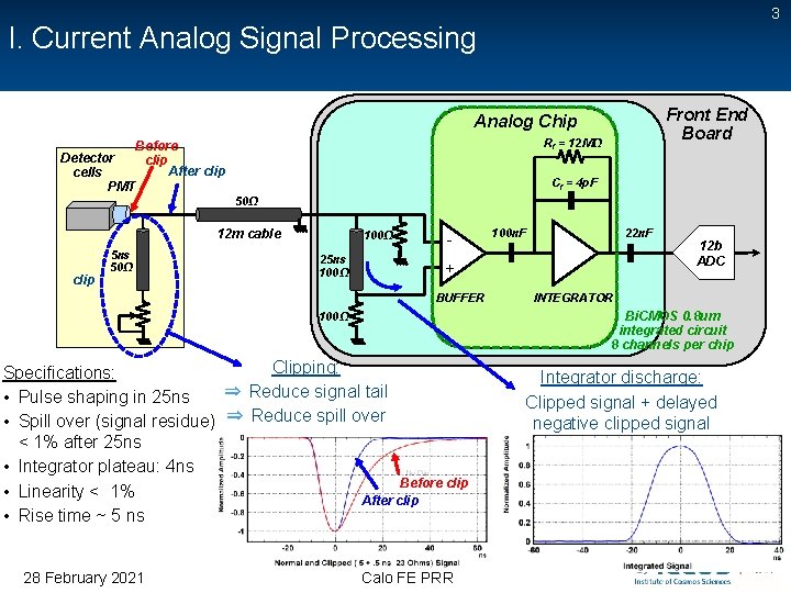
3 I. Current Analog Signal Processing Front End Board Analog Chip Detector cells PMT Rf = 12 MΩ Before clip After clip Cf = 4 p. F 50Ω 12 m cable clip 5 ns 50Ω 100Ω 25 ns 100Ω + BUFFER 12 b ADC INTEGRATOR Bi. CMOS 0. 8 um integrated circuit 8 channels per chip 100Ω Clipping: Specifications: ⇒ Reduce signal tail • Pulse shaping in 25 ns • Spill over (signal residue) ⇒ Reduce spill over < 1% after 25 ns • Integrator plateau: 4 ns Before clip • Linearity < 1% After clip • Rise time ~ 5 ns 28 February 2021 22 n. F 100 n. F Calo FE PRR Integrator discharge: Clipped signal + delayed negative clipped signal

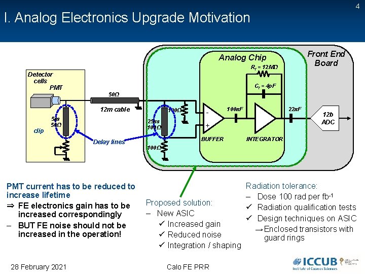
4 I. Analog Electronics Upgrade Motivation Front End Board Analog Chip Rf = 12 MΩ Detector cells PMT Cf = 4 p. F 50Ω 12 m cable clip 5 ns 50Ω 25 ns 100Ω Delay lines PMT current has to be reduced to increase lifetime ⇒ FE electronics gain has to be increased correspondingly – BUT FE noise should not be increased in the operation! 28 February 2021 100Ω - 22 n. F 100 n. F + BUFFER 12 b ADC INTEGRATOR 100Ω Proposed solution: – New ASIC ü Increased gain ü Reduced noise ü Integration / shaping Calo FE PRR Radiation tolerance: – Dose 100 rad per fb-1 ü Radiation qualification tests ü Design techniques on ASIC → Enclosed transistors with guard rings

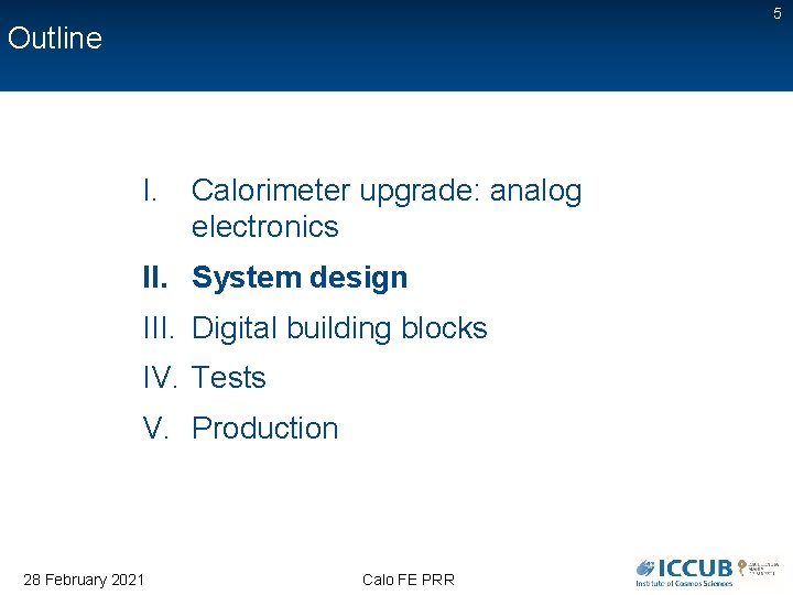
5 Outline I. Calorimeter upgrade: analog electronics II. System design III. Digital building blocks IV. Tests V. Production 28 February 2021 Calo FE PRR

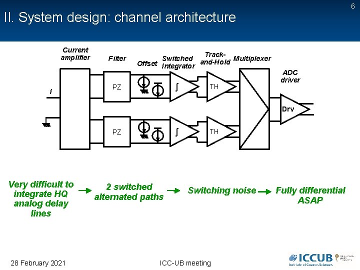
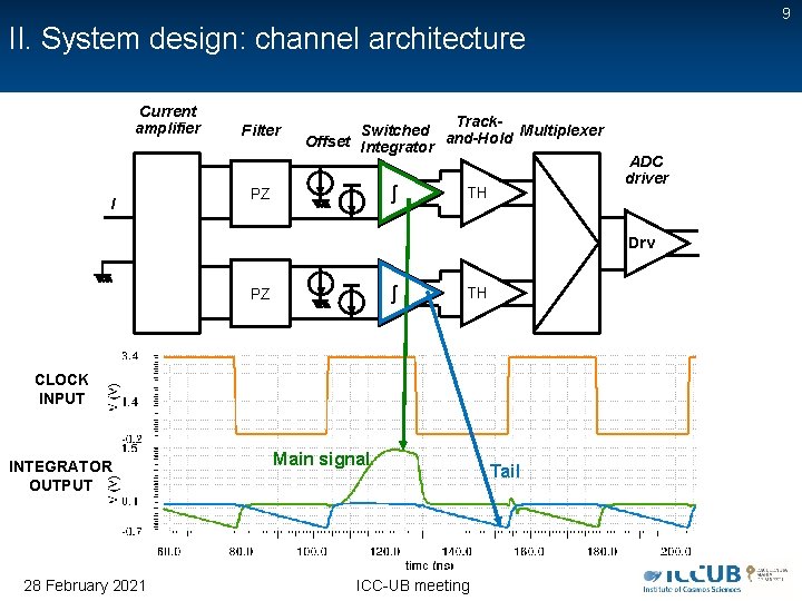
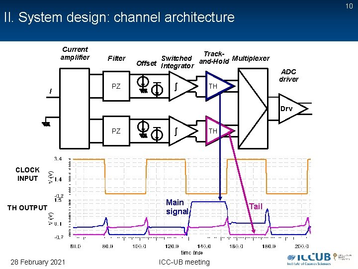
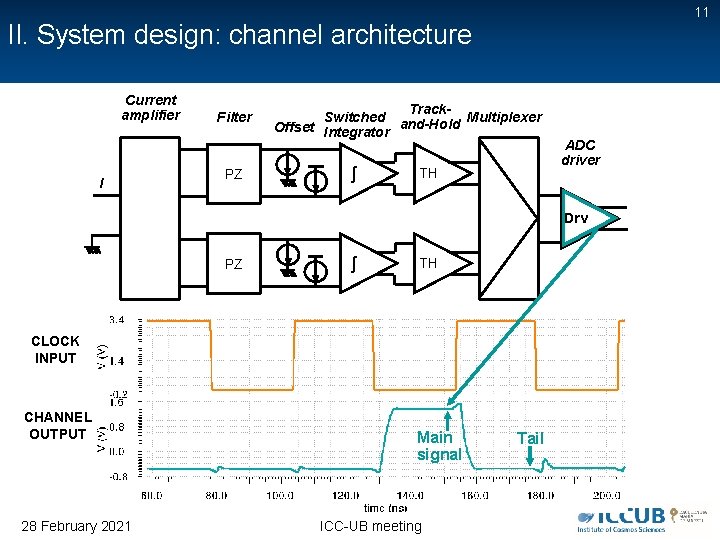
6 II. System design: channel architecture Current amplifier I Filter Track. Switched and-Hold Multiplexer Offset Integrator ʃ PZ TH ADC driver Drv ʃ PZ Very difficult to integrate HQ analog delay lines 28 February 2021 2 switched alternated paths TH Switching noise ICC-UB meeting Fully differential ASAP

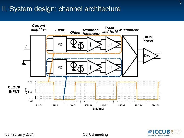
7 II. System design: channel architecture Current amplifier I Filter PZ Track. Switched and-Hold Multiplexer Offset Integrator ʃ TH ADC driver Drv PZ ʃ TH CLOCK INPUT 28 February 2021 ICC-UB meeting

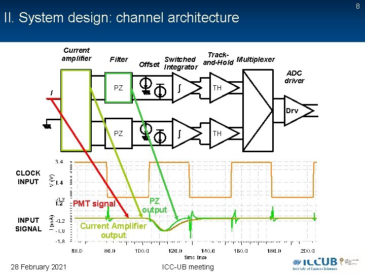
8 II. System design: channel architecture Current amplifier I Filter Track. Switched and-Hold Multiplexer Offset Integrator ʃ PZ TH ADC driver Drv ʃ PZ TH CLOCK INPUT PMT signal INPUT SIGNAL 28 February 2021 PZ output Current Amplifier output ICC-UB meeting

9 II. System design: channel architecture Current amplifier I Filter Track. Switched and-Hold Multiplexer Offset Integrator ʃ PZ TH ADC driver Drv ʃ PZ TH CLOCK INPUT INTEGRATOR OUTPUT 28 February 2021 Main signal ICC-UB meeting Tail

10 II. System design: channel architecture Current amplifier I Filter PZ Track. Switched and-Hold Multiplexer Offset Integrator ʃ TH ADC driver Drv PZ ʃ TH CLOCK INPUT TH OUTPUT 28 February 2021 Main signal ICC-UB meeting Tail

11 II. System design: channel architecture Current amplifier I Filter PZ Track. Switched and-Hold Multiplexer Offset Integrator ʃ TH ADC driver Drv PZ ʃ TH CLOCK INPUT CHANNEL OUTPUT 28 February 2021 Main signal ICC-UB meeting Tail

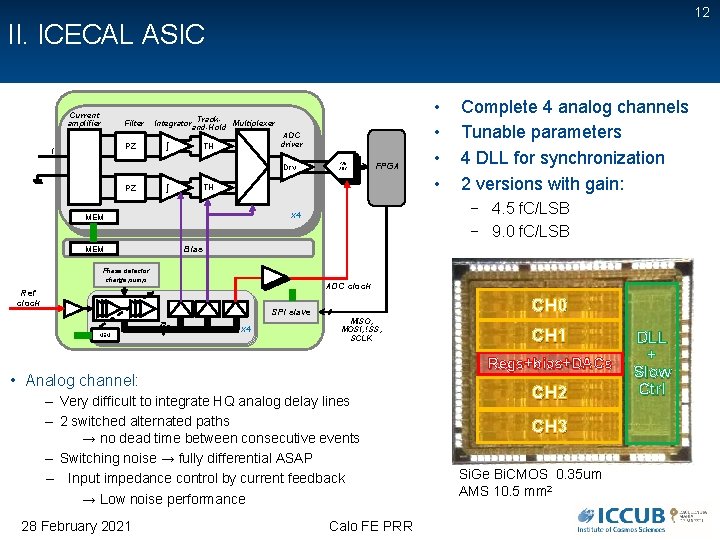
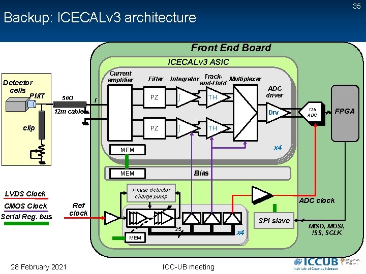
12 II. ICECAL ASIC Current amplifier Filter Integrator Track- Multiplexer and-Hold ʃ PZ I TH ADC driver Drv ʃ PZ FPGA TH Bias MEM Phase detector charge pump ADC clock Ref clock SPI slave 25 x 4 CH 0 MISO, MOSI, !SS, SCLK CH 1 Regs+bias+DACs • Analog channel: – Very difficult to integrate HQ analog delay lines – 2 switched alternated paths → no dead time between consecutive events – Switching noise → fully differential ASAP – Input impedance control by current feedback → Low noise performance 28 February 2021 Complete 4 analog channels Tunable parameters 4 DLL for synchronization 2 versions with gain: − 4. 5 f. C/LSB − 9. 0 f. C/LSB x 4 MEM 12 b 12 b ADC ADC • • Calo FE PRR CH 2 CH 3 Si. Ge Bi. CMOS 0. 35 um AMS 10. 5 mm 2 DLL + Slow Ctrl

13 Outline I. Calorimeter upgrade: analog electronics II. System design III. Digital building blocks IV. Tests V. Production 28 February 2021 Calo FE PRR

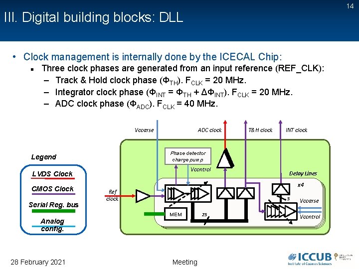
14 III. Digital building blocks: DLL • Clock management is internally done by the ICECAL Chip: Three clock phases are generated from an input reference (REF_CLK): – Track & Hold clock phase (ΦTH). FCLK = 20 MHz. – Integrator clock phase (ΦINT = ΦTH + ΔΦINT). FCLK = 20 MHz. – ADC clock phase (ΦADC). FCLK = 40 MHz. Vcoarse ADC clock Vcontrol LVDS Clock Serial Reg. bus Delay Lines x 4 Ref clock 5 MEM Analog config. 28 February 2021 INT clock Phase detector charge pump Legend CMOS Clock T&H clock Meeting 25 Vcoarse Vcontrol

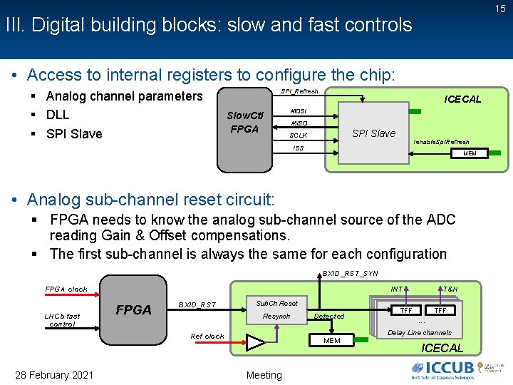
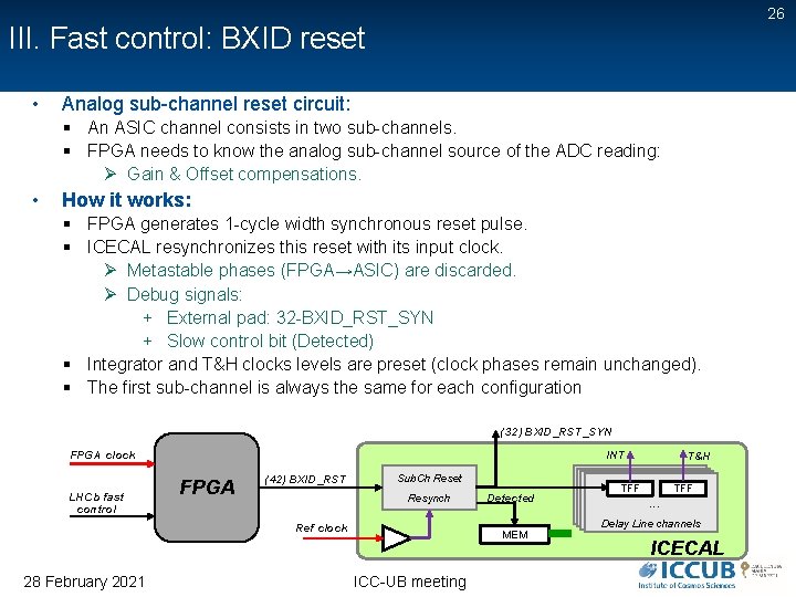
15 III. Digital building blocks: slow and fast controls • Access to internal registers to configure the chip: § Analog channel parameters § DLL § SPI Slave SPI_Refresh Slow. Ctl FPGA ICECAL MOSI MISO SPI Slave SCLK !enable. Spi. Refresh !SS MEM • Analog sub-channel reset circuit: § FPGA needs to know the analog sub-channel source of the ADC reading Gain & Offset compensations. § The first sub-channel is always the same for each configuration BXID_RST_SYN FPGA clock LHCb fast control INT FPGA BXID_RST Sub. Ch Reset Resynch Ref clock 28 February 2021 Detected MEM Meeting TFF T&H TFF ··· Delay Line channels Delay. Linechannels ICECAL

16 Outline I. Calorimeter upgrade: analog electronics II. System design III. Digital building blocks IV. Tests V. Production 28 February 2021 Calo FE PRR

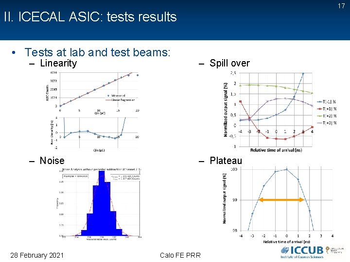
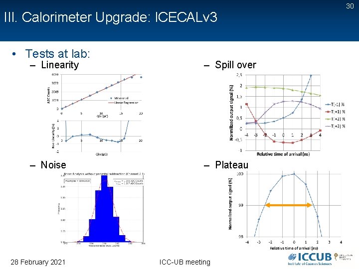
17 II. ICECAL ASIC: tests results • Tests at lab and test beams: – Linearity – Spill over – Noise – Plateau 28 February 2021 Calo FE PRR

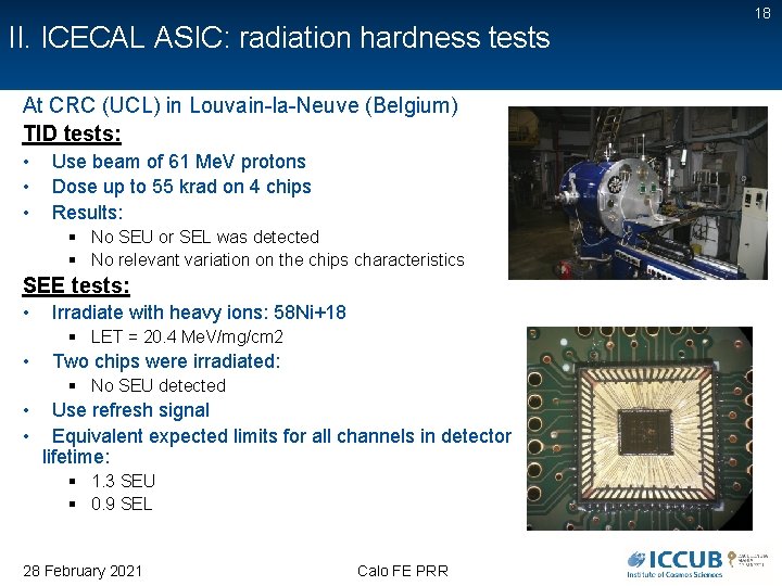
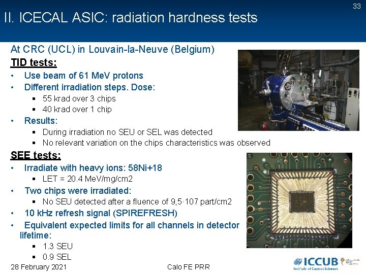
II. ICECAL ASIC: radiation hardness tests At CRC (UCL) in Louvain-la-Neuve (Belgium) TID tests: • • • Use beam of 61 Me. V protons Dose up to 55 krad on 4 chips Results: § No SEU or SEL was detected § No relevant variation on the chips characteristics SEE tests: • Irradiate with heavy ions: 58 Ni+18 § LET = 20. 4 Me. V/mg/cm 2 • Two chips were irradiated: § No SEU detected • • Use refresh signal Equivalent expected limits for all channels in detector lifetime: § 1. 3 SEU § 0. 9 SEL 28 February 2021 Calo FE PRR 18

19 Outline I. Calorimeter upgrade: analog electronics II. System design III. Digital building blocks IV. Tests V. Production 28 February 2021 Calo FE PRR

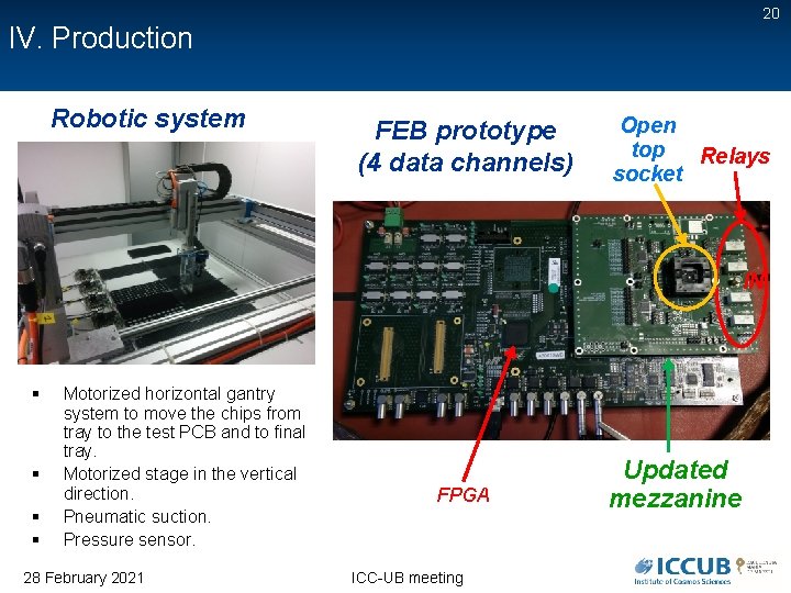
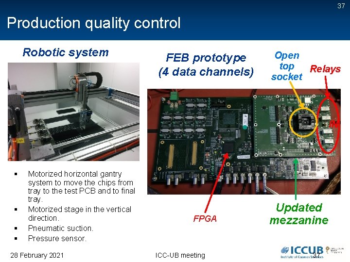
20 IV. Production Robotic system FEB prototype (4 data channels) Open top Relays socket IN § § Motorized horizontal gantry system to move the chips from tray to the test PCB and to final tray. Motorized stage in the vertical direction. Pneumatic suction. Pressure sensor. 28 February 2021 FPGA ICC-UB meeting Updated mezzanine

21 V. Status • Production § § Standard version (v 3. 1): 3050 pieces Reduced gain (v 3. 2): 3050 pieces • Production test § § Mezzanine: ready SW: § Test defined: rejection limits are being prepared § Robotic setup ready in ~2 weeks § Estimated total test time: 2 -3 months 28 February 2021 ICC-UB meeting

22 Backup 28 February 2021 Calo FE PRR

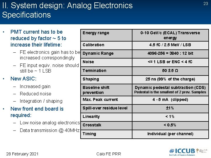
II. System design: Analog Electronics Specifications • PMT current has to be reduced by factor ~ 5 to increase their lifetime: Energy range Calibration – FE electronics gain has to be Dynamic Range increased correspondingly Noise – FE input equiv. noise should Termination still be ~ 1 LSB • New ASIC: – Increased gain • Shaping – Reduced noise Baseline shift prevention – Integration / shaping Max. Peak current New front end board is required: 0 -10 Ge. V/c (ECAL) Transverse energy 4. 5 f. C / 2. 5 Me. V / LSB 4096 -256 = 3840 : 12 bit <≈ 1 LSB or ENC < 4 f. C 50 ± 5 Ω 25 ns (99% of the charge) Dynamic pedestal subtraction (CDS) Pedestal is the smallest of 2 prev. Samples 4 - 5 m. A (clipped) Spill-over residue level ± 1% Linearity < 1% – Low noise analog electronics Crosstalk – Data transmission @ 40 MHz Timing 28 February 2021 23 Calo FE PRR < 0. 5% Individual (per channel)

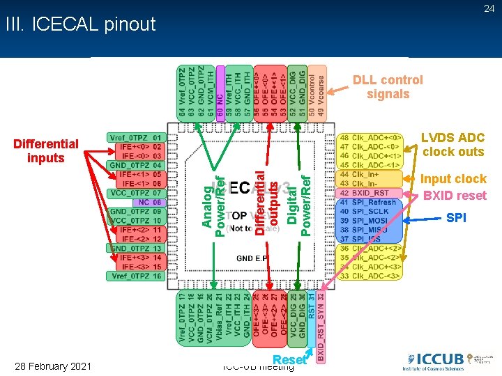
24 III. ICECAL pinout DLL control signals LVDS ADC clock outs 28 February 2021 Digital Power/Ref Differential outputs Analog Power/Ref Differential inputs Reset ICC-UB meeting Input clock BXID reset SPI

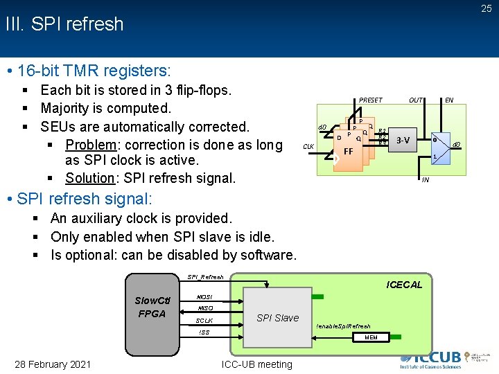
25 III. SPI refresh • 16 -bit TMR registers: § Each bit is stored in 3 flip-flops. § Majority is computed. § SEUs are automatically corrected. § Problem: correction is done as long as SPI clock is active. § Solution: SPI refresh signal. PRESET d 0 CLK P DP Q R 1 DP Q D Q FF R 2 R 3 FF FF 3 -V 0 1 IN • SPI refresh signal: § An auxiliary clock is provided. § Only enabled when SPI slave is idle. § Is optional: can be disabled by software. SPI_Refresh Slow. Ctl FPGA ICECAL MOSI MISO SCLK SPI Slave !SS 28 February 2021 !enable. Spi. Refresh MEM ICC-UB meeting EN OUT d 0

26 III. Fast control: BXID reset • Analog sub-channel reset circuit: § An ASIC channel consists in two sub-channels. § FPGA needs to know the analog sub-channel source of the ADC reading: Ø Gain & Offset compensations. • How it works: § FPGA generates 1 -cycle width synchronous reset pulse. § ICECAL resynchronizes this reset with its input clock. Ø Metastable phases (FPGA→ASIC) are discarded. Ø Debug signals: + External pad: 32 -BXID_RST_SYN + Slow control bit (Detected) § Integrator and T&H clocks levels are preset (clock phases remain unchanged). § The first sub-channel is always the same for each configuration (32) BXID_RST_SYN FPGA clock LHCb fast control INT FPGA (42) BXID_RST Sub. Ch Reset Resynch Ref clock 28 February 2021 Detected MEM ICC-UB meeting TFF T&H TFF ··· Delay Line channels Delay Linechannels ICECAL

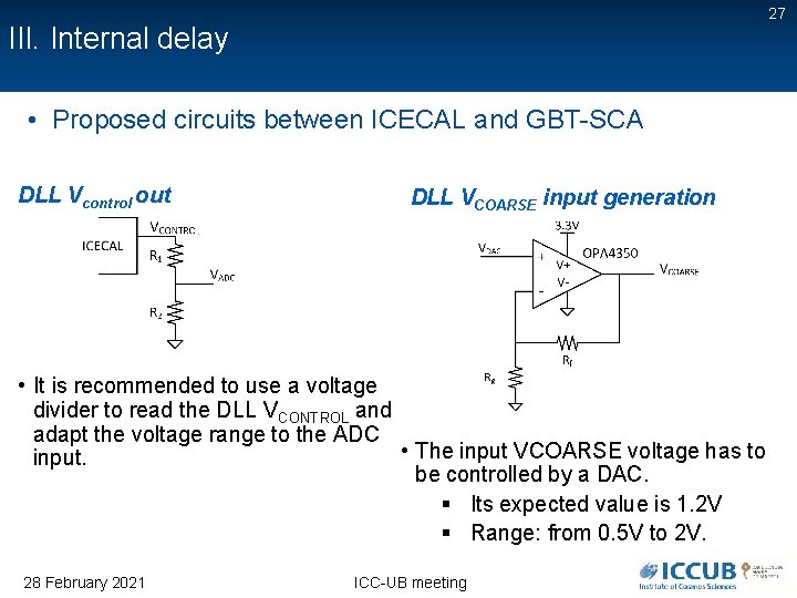
27 III. Internal delay • Proposed circuits between ICECAL and GBT-SCA DLL Vcontrol out DLL VCOARSE input generation • It is recommended to use a voltage divider to read the DLL VCONTROL and adapt the voltage range to the ADC • The input VCOARSE voltage has to input. be controlled by a DAC. § Its expected value is 1. 2 V § Range: from 0. 5 V to 2 V. 28 February 2021 ICC-UB meeting

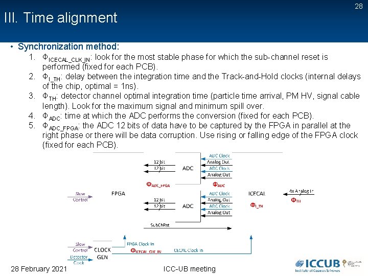
28 III. Time alignment • Synchronization method: 1. ΦICECAL_CLK_IN: look for the most stable phase for which the sub-channel reset is performed (fixed for each PCB). 2. ΦI_TH: delay between the integration time and the Track-and-Hold clocks (internal delays of the chip, optimal = 1 ns). 3. ΦTH: detector channel optimal integration time (particle time arrival, PM HV, signal cable length). Look for the maximum signal and minimum spill over. 4. ΦADC: time at which the ADC performs the conversion (fixed for each PCB). 5. ΦADC_FPGA: the ADC 12 bits of data have to be captured by the FPGA in parallel at the right phase or there will be data corruption. Use rising or falling edge of the FPGA clock (fixed for each PCB). 28 February 2021 ICC-UB meeting 28

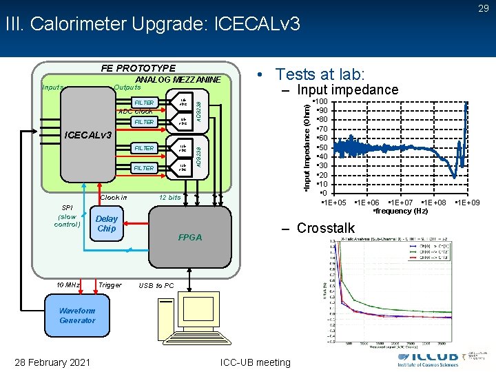
29 III. Calorimeter Upgrade: ICECALv 3 FE PROTOTYPE ANALOG MEZZANINE Outputs ADC clock FILTER 12 b ADC – Input impedance • Input Impedance (Ohm) 12 b ADC FILTER AD 9238 Inputs • Tests at lab: Clock in SPI (slow control) 10 MHz 12 bits Delay Chip Trigger AD 9238 ICECALv 3 FPGA – Crosstalk USB to PC Waveform Generator 28 February 2021 • 100 • 90 • 80 • 70 • 60 • 50 • 40 • 30 • 20 • 10 • 1 E+05 ICC-UB meeting • 1 E+06 • 1 E+07 • 1 E+08 • frequency (Hz) • 1 E+09

III. Calorimeter Upgrade: ICECALv 3 • Tests at lab: – Linearity – Spill over – Noise – Plateau 28 February 2021 ICC-UB meeting 30

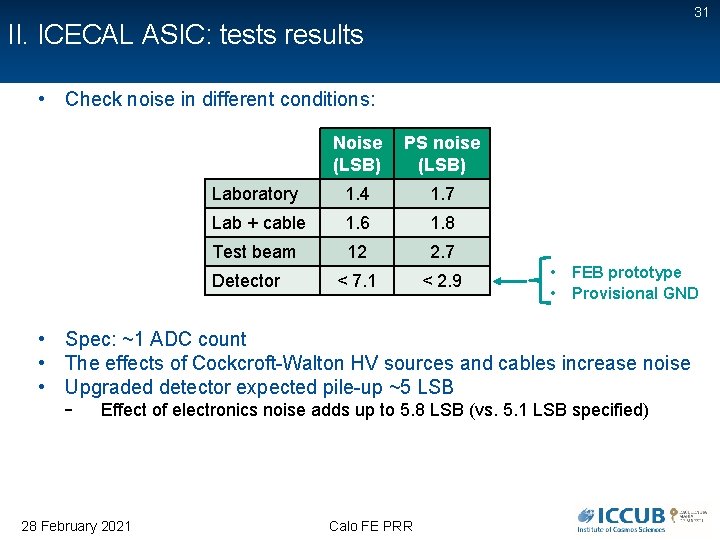
31 II. ICECAL ASIC: tests results • Check noise in different conditions: Noise (LSB) PS noise (LSB) Laboratory 1. 4 1. 7 Lab + cable 1. 6 1. 8 Test beam 12 2. 7 < 7. 1 < 2. 9 Detector • • FEB prototype Provisional GND • Spec: ~1 ADC count • The effects of Cockcroft-Walton HV sources and cables increase noise • Upgraded detector expected pile-up ~5 LSB – Effect of electronics noise adds up to 5. 8 LSB (vs. 5. 1 LSB specified) 28 February 2021 Calo FE PRR

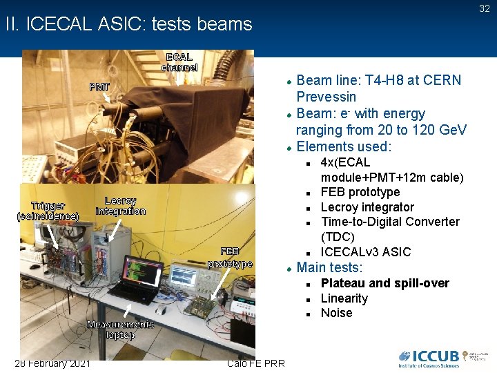
32 II. ICECAL ASIC: tests beams ECAL channel PMT Beam line: T 4 -H 8 at CERN Prevessin Beam: e- with energy ranging from 20 to 120 Ge. V Elements used: Lecroy integration Trigger (coincidence) FEB prototype Main tests: Measurements laptop 28 February 2021 Calo FE PRR 4 x(ECAL module+PMT+12 m cable) FEB prototype Lecroy integrator Time-to-Digital Converter (TDC) ICECALv 3 ASIC Plateau and spill-over Linearity Noise

II. ICECAL ASIC: radiation hardness tests At CRC (UCL) in Louvain-la-Neuve (Belgium) TID tests: • • Use beam of 61 Me. V protons Different irradiation steps. Dose: § 55 krad over 3 chips § 40 krad over 1 chip • Results: § During irradiation no SEU or SEL was detected § No relevant variation on the chips characteristics was observed SEE tests: • Irradiate with heavy ions: 58 Ni+18 § LET = 20. 4 Me. V/mg/cm 2 • Two chips were irradiated: § No SEU detected after a fluence of 9, 5· 107 part/cm 2 • • 10 k. Hz refresh signal (SPIREFRESH) Equivalent expected limits for all channels in detector lifetime: § 1. 3 SEU § 0. 9 SEL 28 February 2021 Calo FE PRR 33

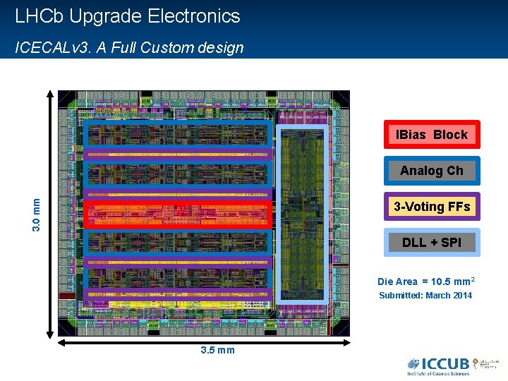
LHCb Upgrade Electronics ICECALv 3. A Full Custom design IBias Block 3. 0 mm Analog Ch 3 -Voting FFs DLL + SPI Die Area = 10. 5 mm 2 Submitted: March 2014 3. 5 mm

35 Backup: ICECALv 3 architecture Front End Board ICECALv 3 ASIC Detector cells PMT Current amplifier 50Ω Filter ʃ PZ I Integrator Track- Multiplexer and-Hold TH 12 m cable Drv clip ʃ PZ Serial Reg. bus Bias Phase detector charge pump ADC clock Ref clock SPI slave 25 MEM 28 February 2021 FPGA x 4 MEM LVDS Clock 12 b 12 b ADC ADC TH MEM CMOS Clock ADC driver ICC-UB meeting x 4 MISO, MOSI, !SS, SCLK

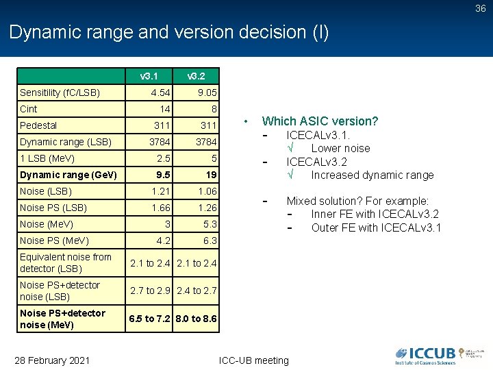
36 Dynamic range and version decision (I) v 3. 1 Sensitility (f. C/LSB) v 3. 2 4. 54 9. 05 14 8 311 3784 1 LSB (Me. V) 2. 5 5 Dynamic range (Ge. V) 9. 5 19 Noise (LSB) 1. 21 1. 06 Noise PS (LSB) 1. 66 1. 26 3 5. 3 4. 2 6. 3 Cint Pedestal Dynamic range (LSB) Noise (Me. V) Noise PS (Me. V) Equivalent noise from detector (LSB) 2. 1 to 2. 4 Noise PS+detector noise (LSB) 2. 7 to 2. 9 2. 4 to 2. 7 Noise PS+detector noise (Me. V) 6. 5 to 7. 2 8. 0 to 8. 6 28 February 2021 • Which ASIC version? – – – ICECALv 3. 1. √ Lower noise ICECALv 3. 2 √ Increased dynamic range Mixed solution? For example: – Inner FE with ICECALv 3. 2 – Outer FE with ICECALv 3. 1 ICC-UB meeting

37 Production quality control Robotic system FEB prototype (4 data channels) Open top Relays socket IN § § Motorized horizontal gantry system to move the chips from tray to the test PCB and to final tray. Motorized stage in the vertical direction. Pneumatic suction. Pressure sensor. 28 February 2021 FPGA ICC-UB meeting Updated mezzanine 37

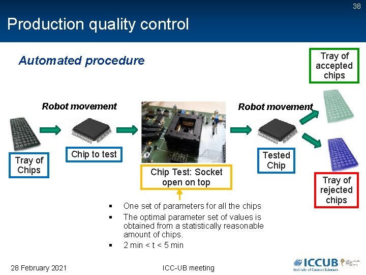
38 Production quality control Tray of accepted chips Automated procedure Robot movement Tray of Chips Chip to test Chip Test: Socket open on top § § § 28 February 2021 Robot movement Tested Chip One set of parameters for all the chips The optimal parameter set of values is obtained from a statistically reasonable amount of chips. 2 min < t < 5 min ICC-UB meeting Tray of rejected chips

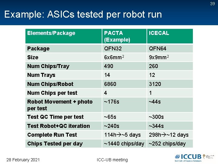
39 Example: ASICs tested per robot run Elements/Package PACTA (Example) ICECAL Package QFN 32 QFN 64 Size 6 x 6 mm 2 9 x 9 mm 2 Num Chips/Tray 490 260 Num Trays 14 12 Num Chips/Robot 6860 3120 Num Chips per test 4 1 Robot Movement + photo per test ~176 s ~44 s Test QC Time per test ~65 s ~300 s Test Robot+QC iteration ~240 s ~344 s Complete Run Test 114 h ~5 days 298 h ~12 days Chips Tested per day ~1440 chips/day ~252 chips/day 28 February 2021 ICC-UB meeting