TRANSISTOR AMPLIFIER CONFIGURATION COMMON EMITTER AMPLIFIER Introduction l

- Slides: 52

TRANSISTOR AMPLIFIER CONFIGURATION COMMON – EMITTER AMPLIFIER

Introduction l 3 basic single-transistor amplifier configuration that can be formed are: Common-emitter (C-E configuration) l Common collector / emitter follower (C-C configuration) l Common base (C-B configuration) l l Each configuration has its own advantages in form of: Input impedance l Output impedance l Current / voltage amplification l

Basic BJT Amplifier

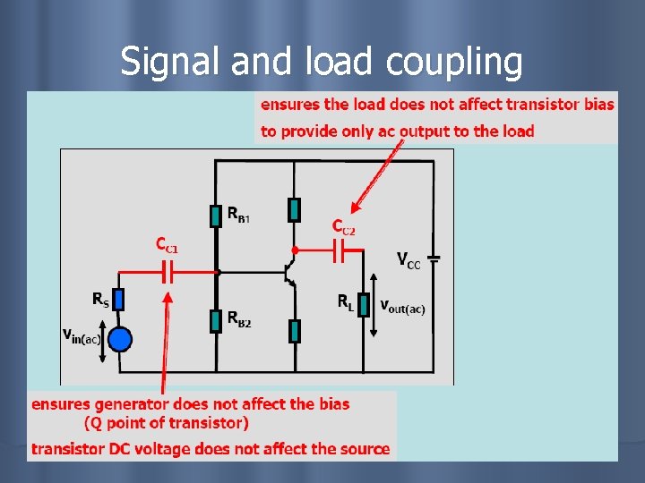
Signal and load coupling

Basic amplifier dc analysis

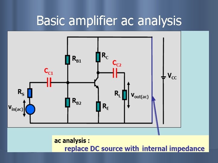
Basic amplifier ac analysis

Common-emitter amplifier

Common-collector amplifier

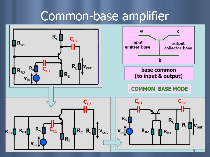
Common-base amplifier

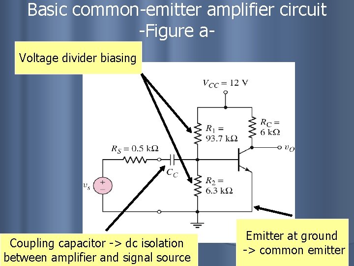
Basic common-emitter amplifier circuit -Figure a. Voltage divider biasing Coupling capacitor -> dc isolation between amplifier and signal source Emitter at ground -> common emitter

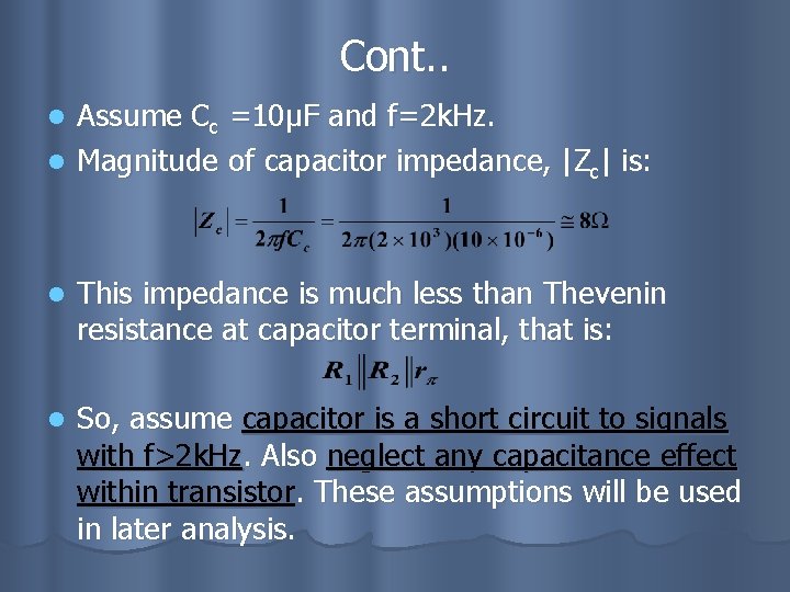
Cont. . Assume Cc =10μF and f=2 k. Hz. l Magnitude of capacitor impedance, |Zc| is: l l This impedance is much less than Thevenin resistance at capacitor terminal, that is: l So, assume capacitor is a short circuit to signals with f>2 k. Hz. Also neglect any capacitance effect within transistor. These assumptions will be used in later analysis.

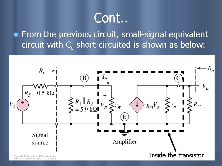
Cont. . l From the previous circuit, small-signal equivalent circuit with Cc short-circuited is shown as below: Inside the transistor

Cont. .

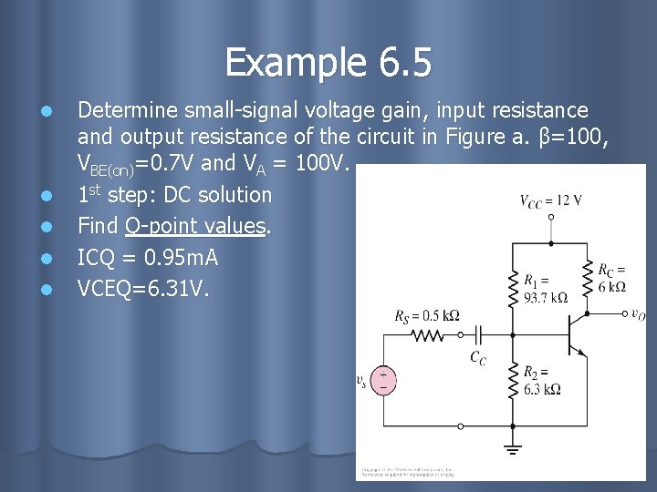
Example 6. 5 l l l Determine small-signal voltage gain, input resistance and output resistance of the circuit in Figure a. β=100, VBE(on)=0. 7 V and VA = 100 V. 1 st step: DC solution Find Q-point values. ICQ = 0. 95 m. A VCEQ=6. 31 V.

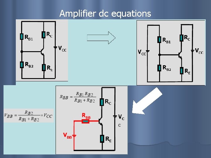
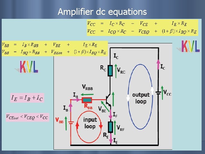
Amplifier dc equations

Amplifier dc equations

Amplifier dc equations

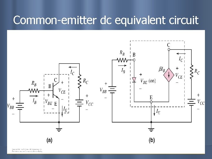
Common-emitter dc equivalent circuit

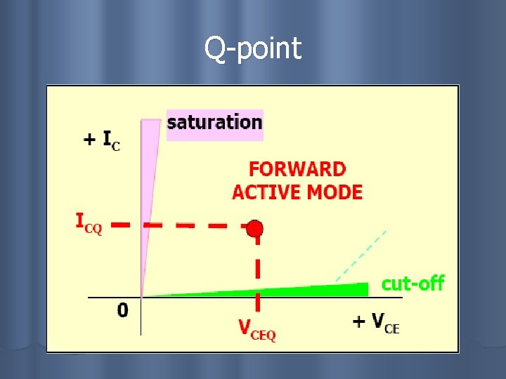
Q-point

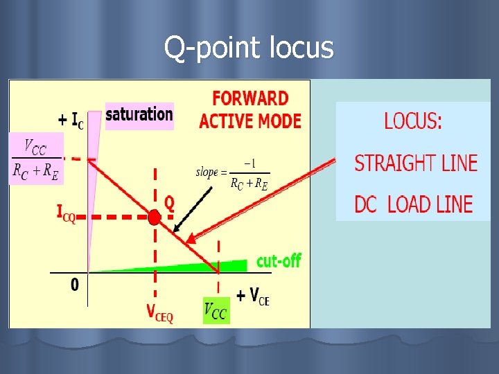
Q-point locus

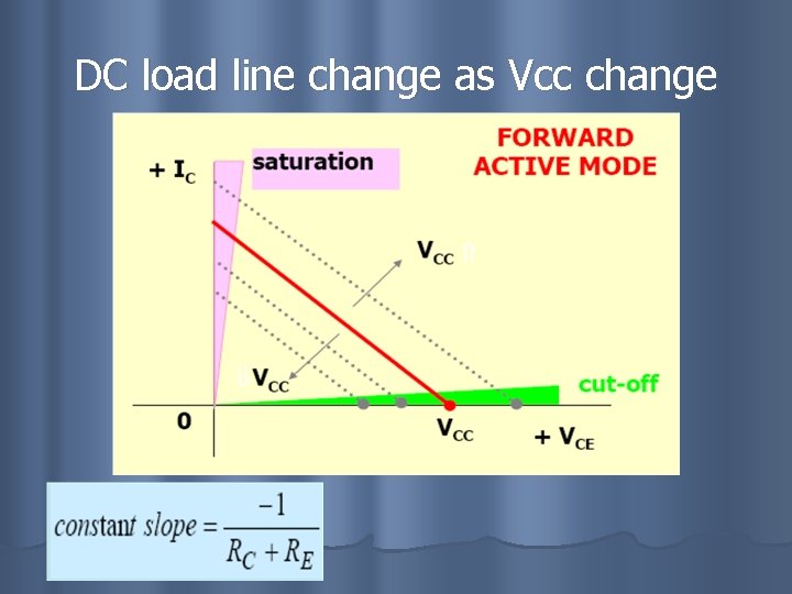
DC load line change as Vcc change

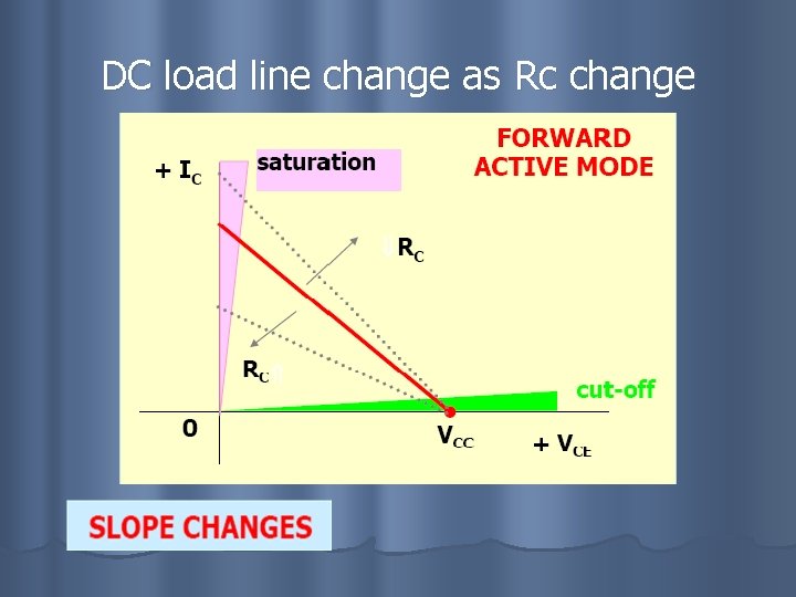
DC load line change as Rc change

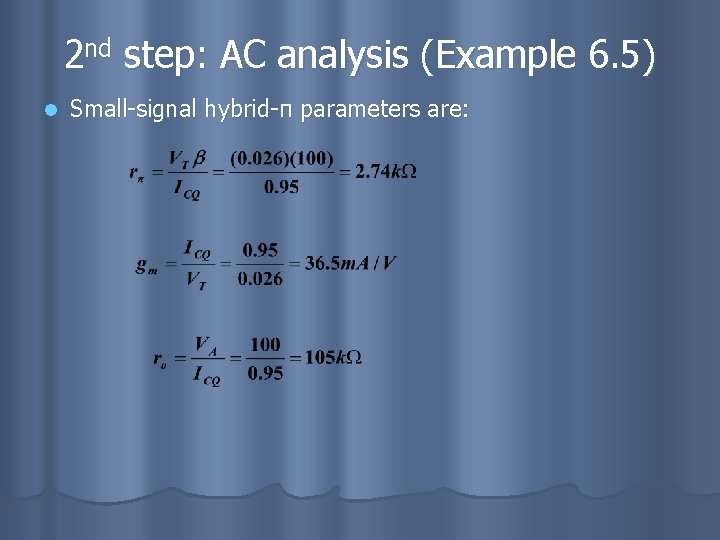
2 nd step: AC analysis (Example 6. 5) l Small-signal hybrid-π parameters are:

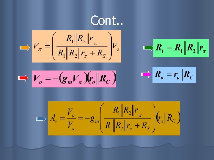
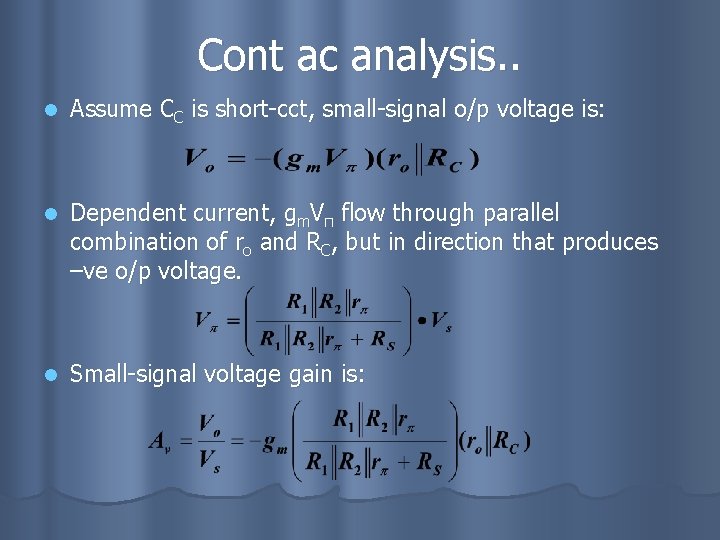
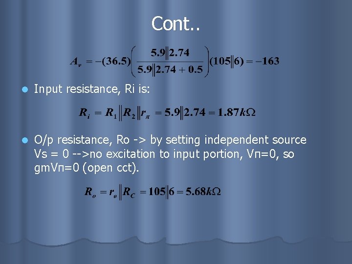
Cont ac analysis. . l Assume CC is short-cct, small-signal o/p voltage is: l Dependent current, gm. Vπ flow through parallel combination of ro and RC, but in direction that produces –ve o/p voltage. l Small-signal voltage gain is:

Cont. . l Input resistance, Ri is: l O/p resistance, Ro -> by setting independent source Vs = 0 -->no excitation to input portion, Vπ=0, so gm. Vπ=0 (open cct).

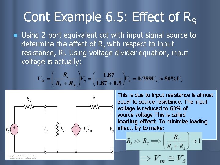
Cont Example 6. 5: Effect of RS l Using 2 -port equivalent cct with input signal source to determine the effect of RS with respect to input resistance, Ri. Using voltage divider equation, input voltage is actually: This is due to input resistance is almost equal to source resistance. The input voltage is reduced to 80% of source voltage. This is called loading effect. To minimize loading effect, try to make:

C-E with emitter resistor l l The basic common-emitter used in previous analysis cause a serious problem when: If BJT with VBE=0. 7 V is used, we get IB=9. 5μA and IC=0. 95 m. A but. . If a new BJT with VBE=0. 6 V is used, IB=26μA will make transistor goes into saturation not practical. Improved design include an emitter resistor.

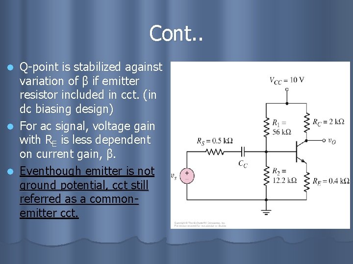
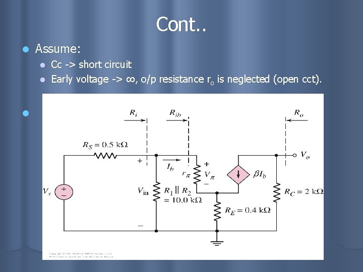
Cont. . Q-point is stabilized against variation of β if emitter resistor included in cct. (in dc biasing design) l For ac signal, voltage gain with RE is less dependent on current gain, β. l Eventhough emitter is not ground potential, cct still referred as a commonemitter cct. l

Cont. . l Assume: Cc -> short circuit l Early voltage -> ∞, o/p resistance ro is neglected (open cct). l l

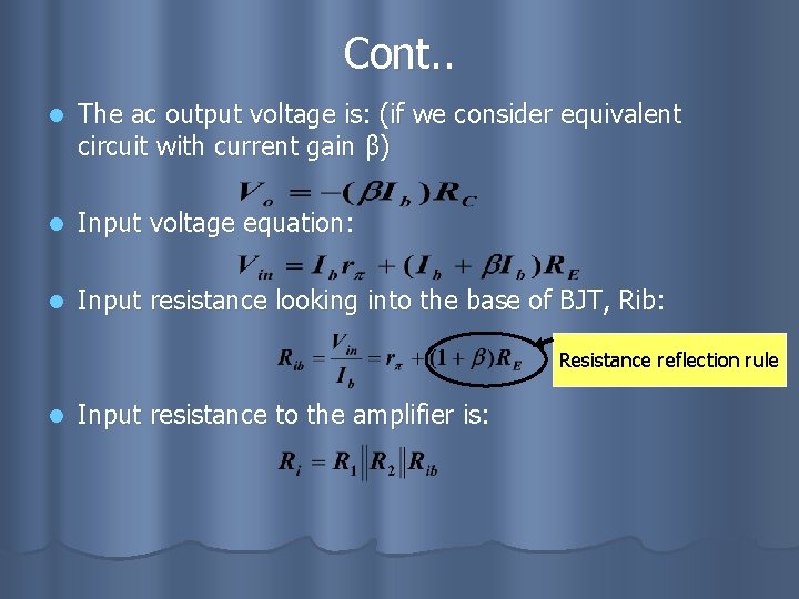
Cont. . l The ac output voltage is: (if we consider equivalent circuit with current gain β) l Input voltage equation: l Input resistance looking into the base of BJT, Rib: Resistance reflection rule l Input resistance to the amplifier is:

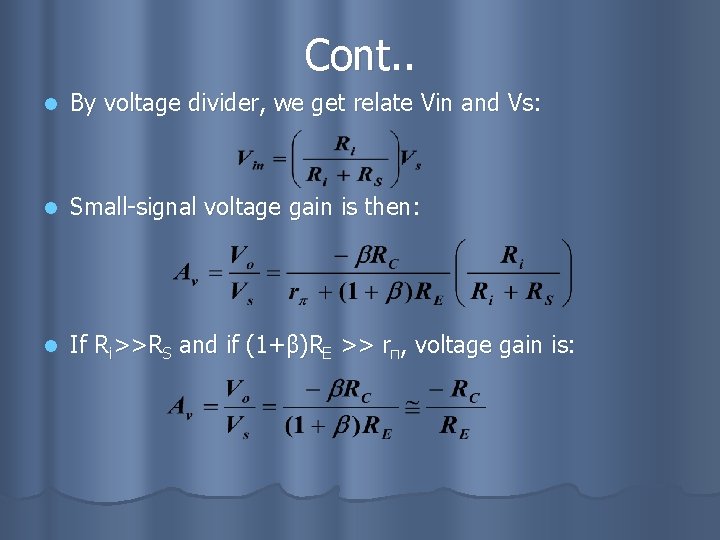
Cont. . l By voltage divider, we get relate Vin and Vs: l Small-signal voltage gain is then: l If Ri>>RS and if (1+β)RE >> rπ, voltage gain is:

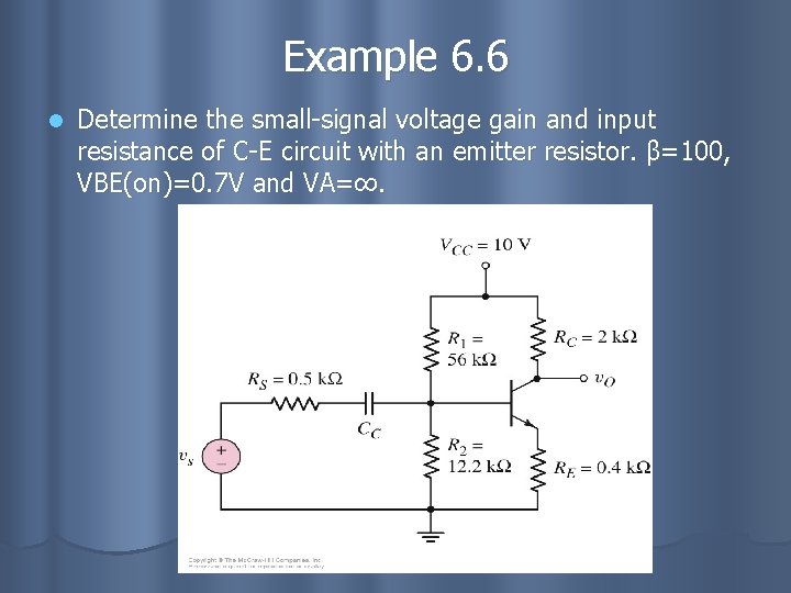
Example 6. 6 l Determine the small-signal voltage gain and input resistance of C-E circuit with an emitter resistor. β=100, VBE(on)=0. 7 V and VA=∞.

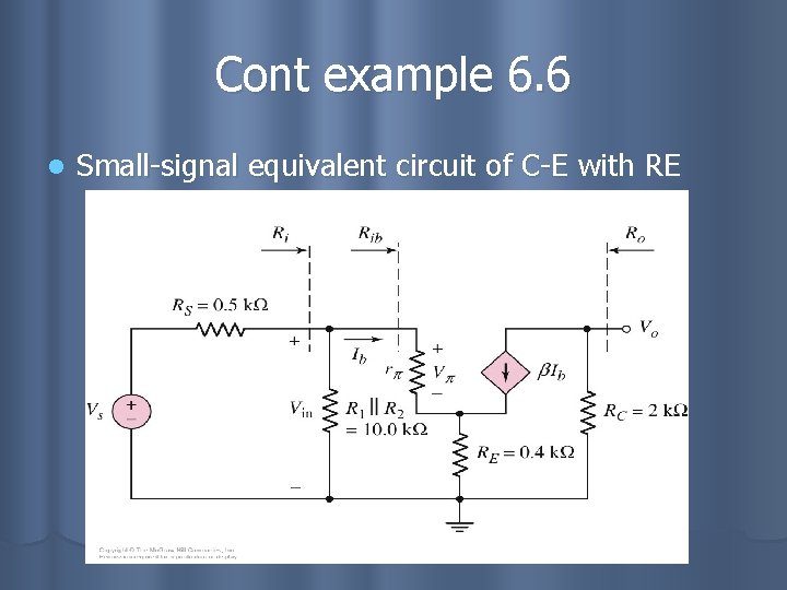
Cont example 6. 6 l Small-signal equivalent circuit of C-E with RE

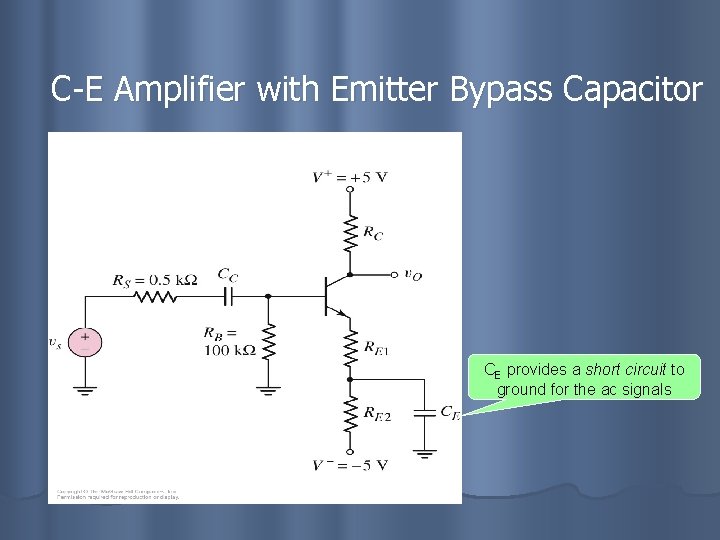
C-E Amplifier with Emitter Bypass Capacitor CE provides a short circuit to ground for the ac signals

Cont. . By include RE, it provide stability of Q-point. l If RE is too high +++> small-signal voltage gain will be reduced severely. (see Av equation) l l l Thus, RE is split to RE 1 & RE 2 and the second resistor is bypassed with “emitter bypass capacitor”. CE provides a short circuit to ground for ac signal. So, only RE 1 is a part of ac equivalent circuit. For dc stability: RE=RE 1+RE 2 For ac gain stability: RE=RE 1 since CE will short RE 2 to ground.

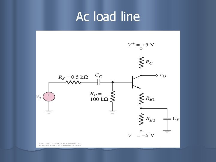
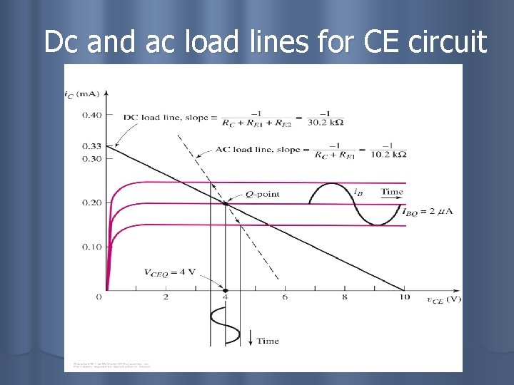
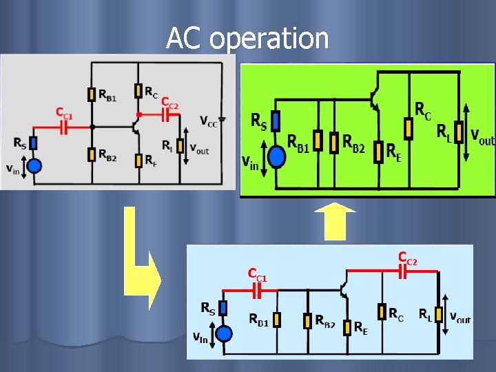
AC Load Line Analysis l l Dc load line -> a way of visualizing r/ship between Q-point and transistor characteristic. When capacitor included in cct, a new effective load line ac load line exist. Ac load line -> visualizing r/ship between smallsignal response and transistor characteristic. Ac operating region is on ac load line.

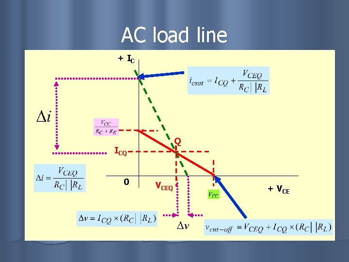
Ac load line

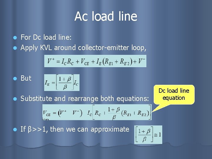
Ac load line For Dc load line: l Apply KVL around collector-emitter loop, l l But l Substitute and rearrange both equations: l If β>>1, then we can approximate Dc load line equation

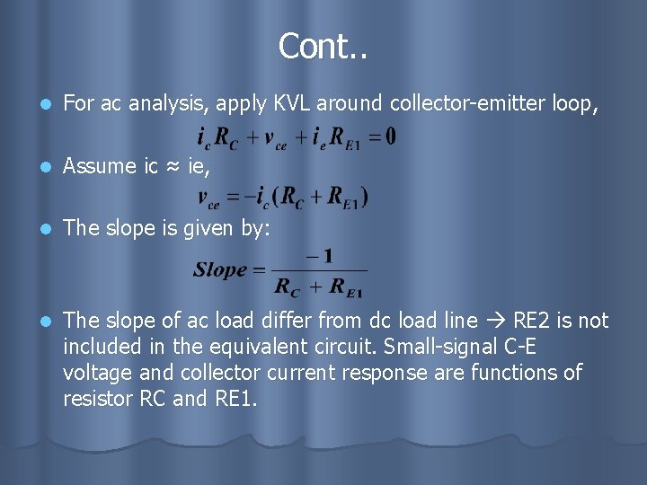
Cont. . l For ac analysis, apply KVL around collector-emitter loop, l Assume ic ≈ ie, l The slope is given by: l The slope of ac load differ from dc load line RE 2 is not included in the equivalent circuit. Small-signal C-E voltage and collector current response are functions of resistor RC and RE 1.

Dc and ac load lines for CE circuit

AC operation

AC load line + IC Q ICQ 0 VCEQ + VCE

WAVEFORMS

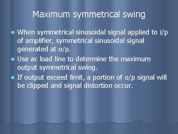
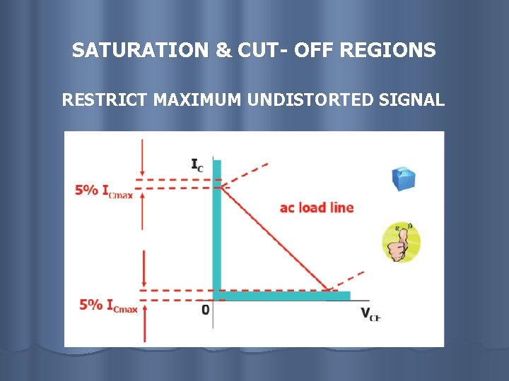
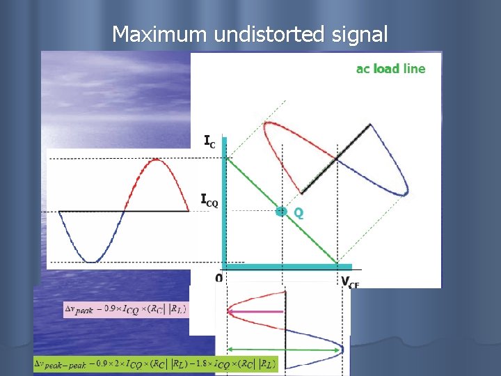
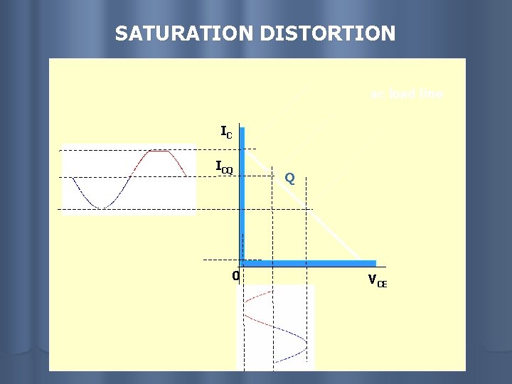
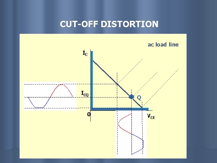
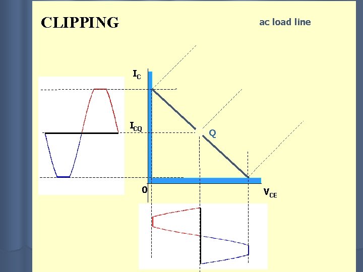
Maximum symmetrical swing When symmetrical sinusoidal signal applied to i/p of amplifier, symmetrical sinusoidal signal generated at o/p. l Use ac load line to determine the maximum output symmetrical swing. l If output exceed limit, a portion of o/p signal will be clipped and signal distortion occur. l

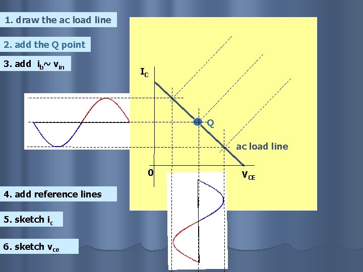
1. draw the ac load line 2. add the Q point 3. add ib~ vin IC Q ac load line 0 4. add reference lines 5. sketch ic 6. sketch vce VCE

SATURATION & CUT- OFF REGIONS RESTRICT MAXIMUM UNDISTORTED SIGNAL

Maximum undistorted signal

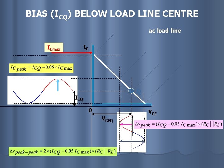
BIAS (ICQ) BELOW LOAD LINE CENTRE ac load line IC ICmax Q ICQ 0 VCEQ VCE

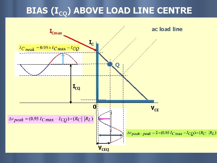
BIAS (ICQ) ABOVE LOAD LINE CENTRE ac load line ICmax IC Q ICQ 0 VCEQ

SATURATION DISTORTION ac load line IC ICQ 0 Q VCE

CUT-OFF DISTORTION ac load line IC ICQ 0 Q VCE

CLIPPING ac load line IC ICQ 0 Q VCE