Emitter Followers The commoncollector or emitter follower amplifier

- Slides: 20

Emitter Followers

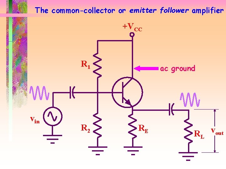
The common-collector or emitter follower amplifier +VCC R 1 vin R 2 ac ground RE RL vout

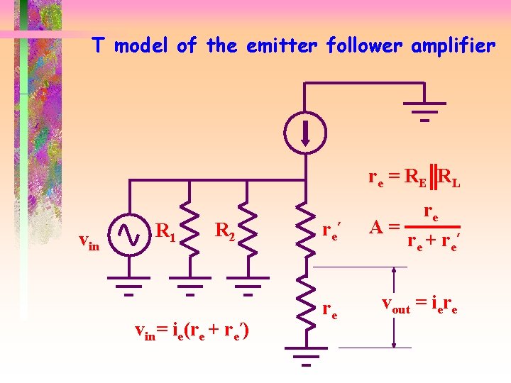
T model of the emitter follower amplifier r e = R E RL vin R 1 R 2 vin= ie(re + re’) r e’ re A= r e + r e’ re vout = iere

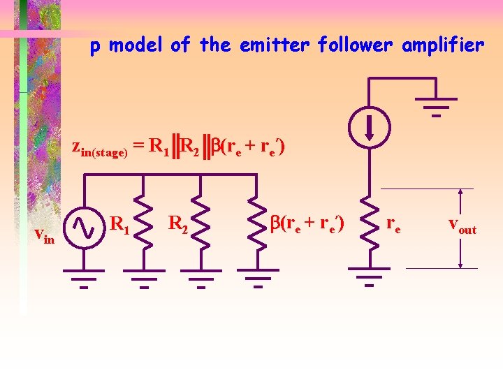
p model of the emitter follower amplifier zin(stage) = R 1 R 2 b(re + re’) vin R 1 R 2 b(re + re’) re vout

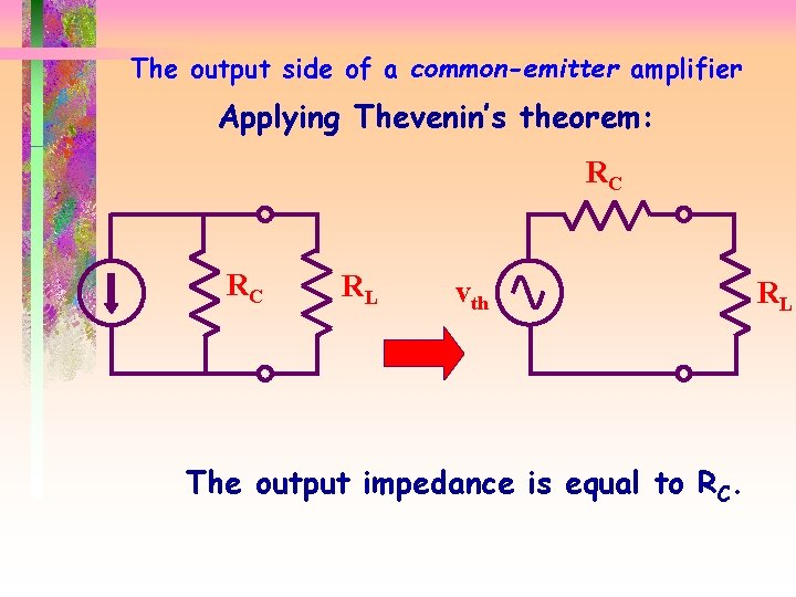
The output side of a common-emitter amplifier Applying Thevenin’s theorem: RC RC RL vth The output impedance is equal to RC. RL

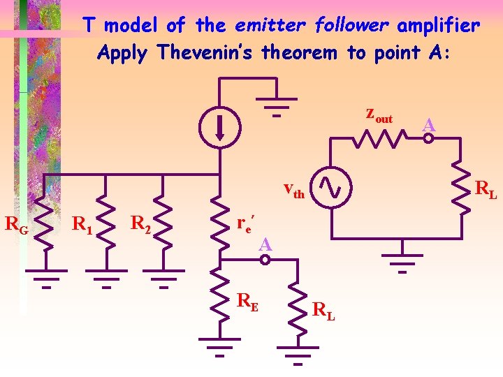
T model of the emitter follower amplifier Apply Thevenin’s theorem to point A: zout vth RG R 1 R 2 r e’ RL A RE A RL

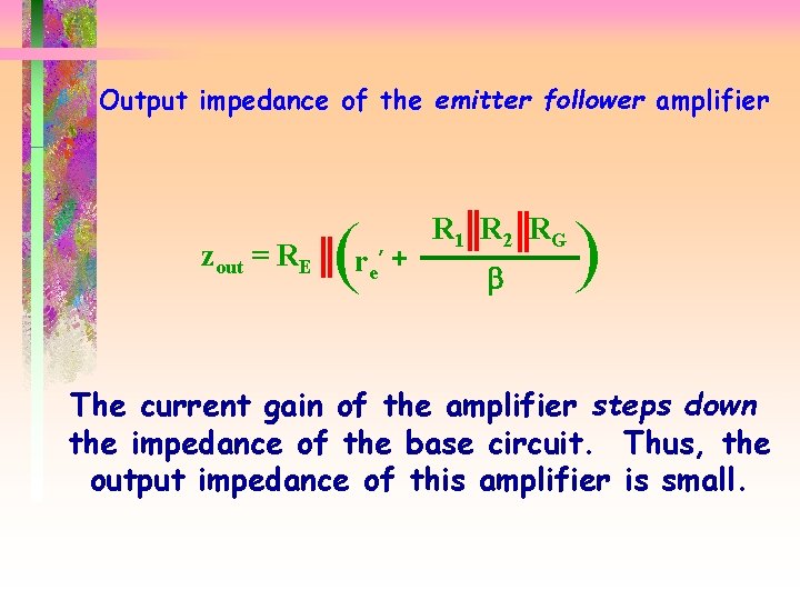
Output impedance of the emitter follower amplifier zout = RE ( r e’ + R 1 R 2 RG b ) The current gain of the amplifier steps down the impedance of the base circuit. Thus, the output impedance of this amplifier is small.

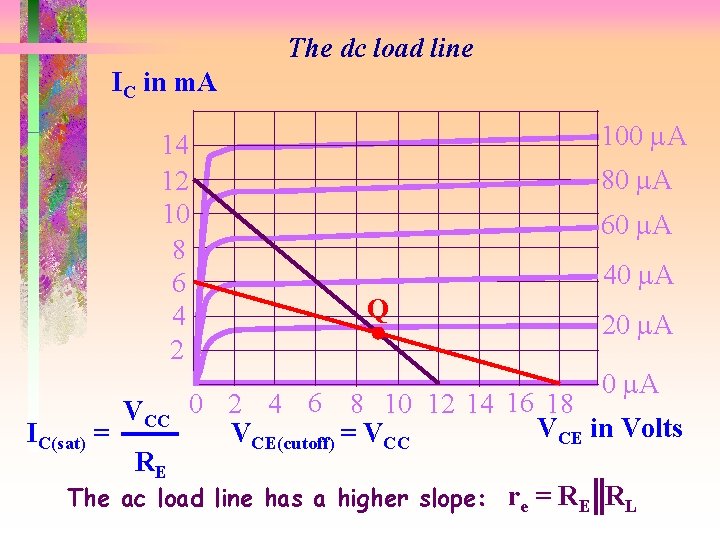
The dc load line IC in m. A 14 12 10 8 6 4 2 100 m. A 80 m. A 60 m. A 40 m. A Q 20 m. A VCC 0 2 4 6 8 10 12 14 16 18 VCE in Volts IC(sat) = VCE(cutoff) = VCC RE The ac load line has a higher slope: re = RE RL

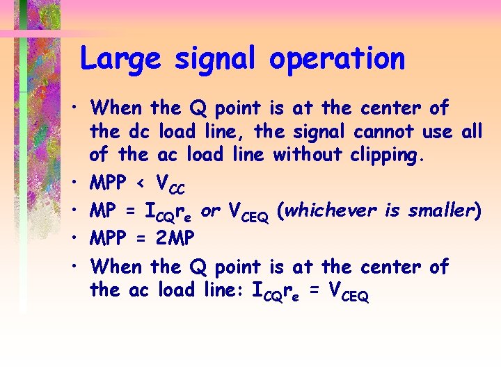
Large signal operation • When the Q point is at the center of the dc load line, the signal cannot use all of the ac load line without clipping. • MPP < VCC • MP = ICQre or VCEQ (whichever is smaller) • MPP = 2 MP • When the Q point is at the center of the ac load line: ICQre = VCEQ

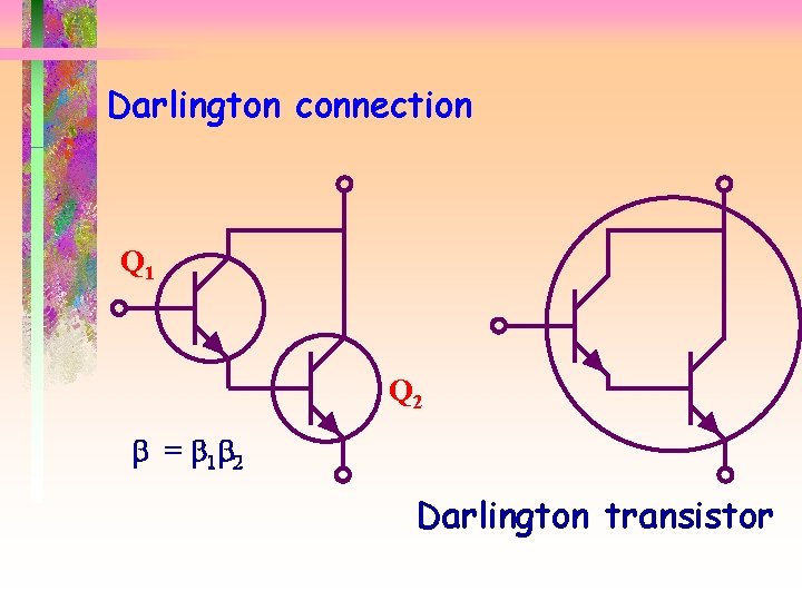
Darlington connection Q 1 Q 2 b = b 1 b 2 Darlington transistor

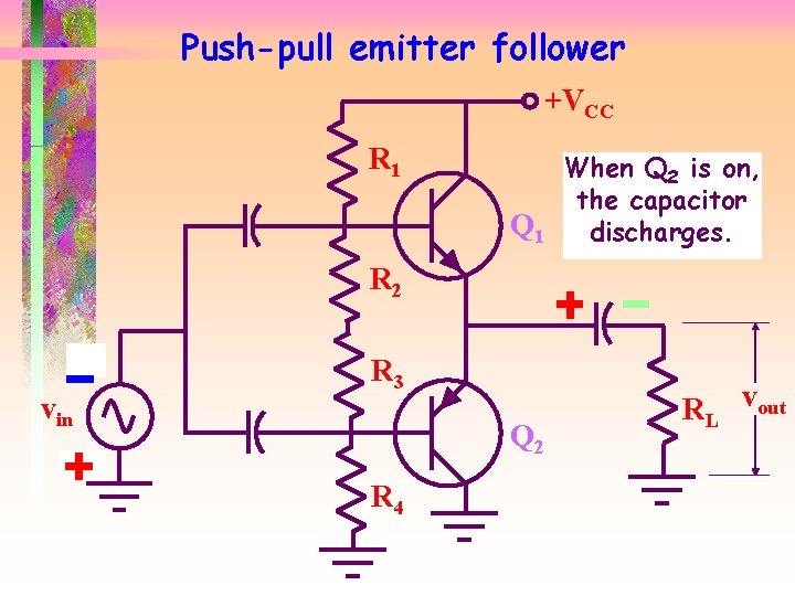
Push-pull emitter follower +VCC R 1 Q 1 When ison, When Q Q 21 is the capacitor discharges. R 2 vin R 3 Q 2 R 4 RL vout

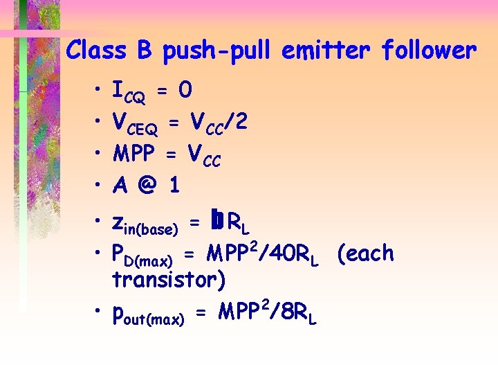
Class B push-pull emitter follower • • ICQ = 0 VCEQ = VCC/2 MPP = VCC A @ 1 • zin(base) = b RL • PD(max) = MPP 2/40 RL (each transistor) 2 • pout(max) = MPP /8 RL

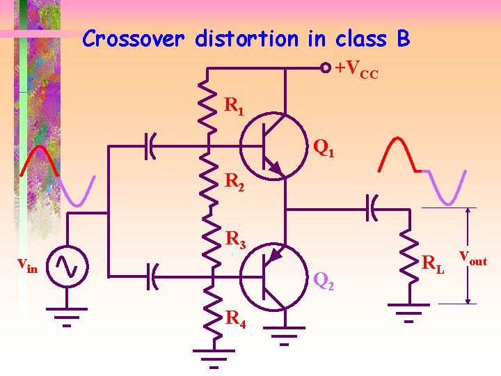
Crossover distortion in class B +VCC R 1 Q 1 R 2 vin R 3 Q 2 R 4 RL vout

Class AB • Crossover distortion is caused by the barrier potential of the emitter diodes. • ICQ must be increased to 1 to 5 percent of IC(sat) to eliminate crossover distortion. • The new operating point is between class A and B but is much closer to B.

Thermal runaway • When temperature increases, collector current increases. • More current produces more heat. • Compensating diodes that match the VBE curves of the transistors are often used. • Any increase in temperature reduces the bias developed across the diodes.

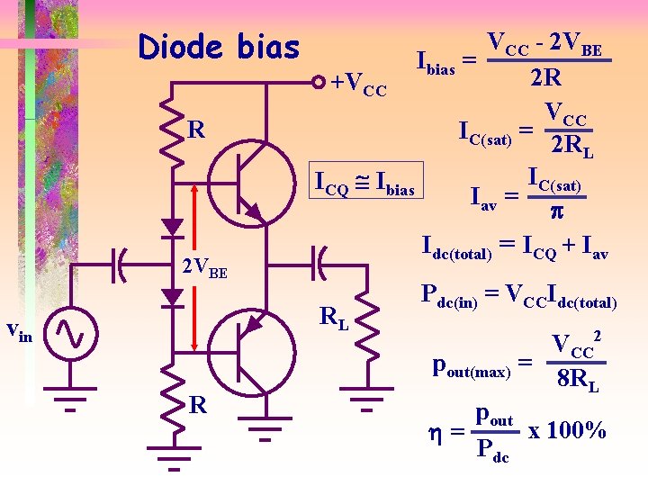
Diode bias R 2 VBE VCC - 2 VBE Ibias = 2 R +VCC IC(sat) = 2 RL IC(sat) ICQ @ Ibias Iav = p Idc(total) = ICQ + Iav RL vin R Pdc(in) = VCCIdc(total) VCC 2 pout(max) = 8 RL pout x 100% h= Pdc

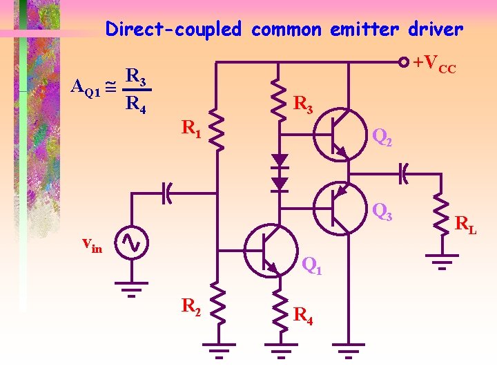
Direct-coupled common emitter driver R 3 AQ 1 @ R 4 +VCC R 1 R 3 Q 2 Q 3 vin Q 1 R 2 R 4 RL

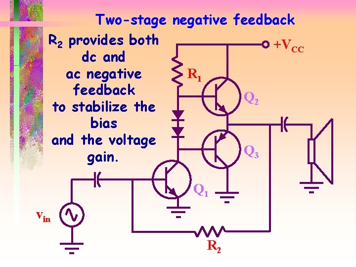
Two-stage negative feedback R 2 provides both +VCC dc and ac negative R 1 feedback Q 2 to stabilize the bias and the voltage Q 3 gain. Q 1 vin R 2

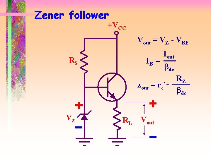
Zener follower +VCC Vout = VZ - VBE RS IB = Iout bdc zout = re’ + VZ RL Vout RZ bdc

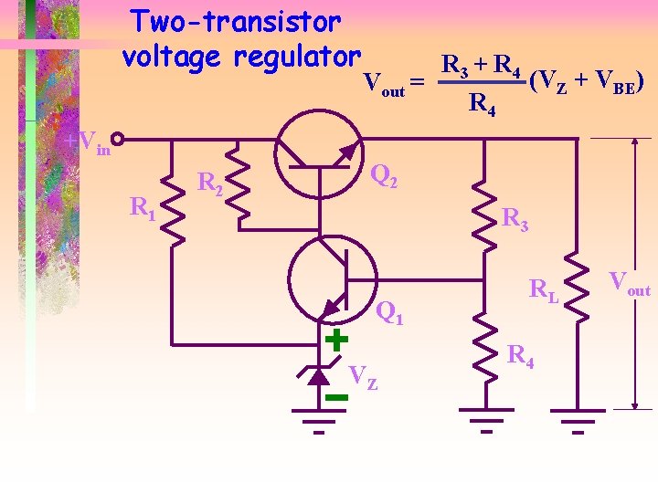
Two-transistor voltage regulator R 3 + R 4 (VZ + VBE) Vout = R 4 +Vin R 1 R 2 Q 2 R 3 Q 1 VZ RL R 4 Vout