FPGA Implementation of Denoising in OFDM Systems using

- Slides: 23

FPGA Implementation of Denoising in OFDM Systems using DSP Design Module Prof. Brian L. Evans Ph. D Students Jing Lin, Yousof Mortazavi, Marcel Nassar & Karl Nieman Wireless Networking and Communications Group Department of Electrical and Computer Engineering Cockrell School of Engineering The University of Texas at Austin May 10, 2012

Outline | Background | System Design and Implementation | Conclusions Outline Part I • Algorithm Description • Project Goals • System Design and Implementation Part II • Demonstration Part III • Conclusions and Discussion 1

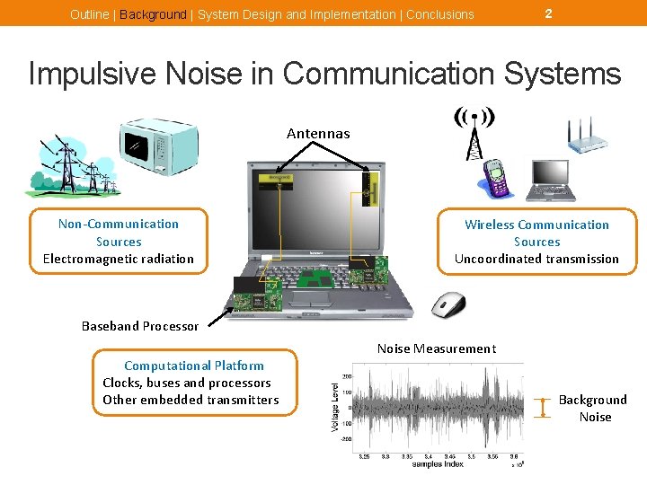
Outline | Background | System Design and Implementation | Conclusions 2 Impulsive Noise in Communication Systems Antennas Non-Communication Sources Electromagnetic radiation Wireless Communication Sources Uncoordinated transmission Baseband Processor Computational Platform Clocks, buses and processors Other embedded transmitters Noise Measurement Background Noise

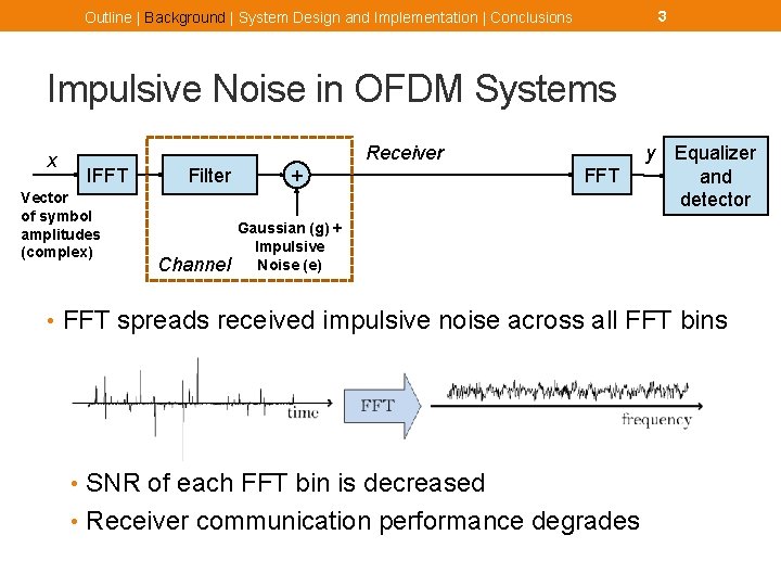
3 Outline | Background | System Design and Implementation | Conclusions Impulsive Noise in OFDM Systems x Receiver IFFT Vector of symbol amplitudes (complex) Filter Channel + y FFT Equalizer and detector Gaussian (g) + Impulsive Noise (e) • FFT spreads received impulsive noise across all FFT bins • SNR of each FFT bin is decreased • Receiver communication performance degrades

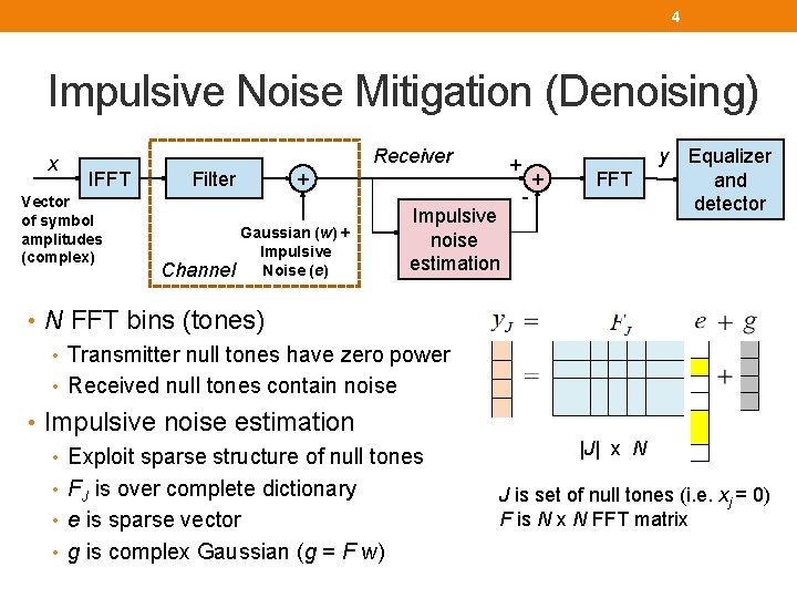
4 Impulsive Noise Mitigation (Denoising) x Receiver IFFT Vector of symbol amplitudes (complex) Filter Channel + Gaussian (w) + Impulsive Noise (e) y + Impulsive noise estimation - + FFT Equalizer and detector • N FFT bins (tones) • Transmitter null tones have zero power • Received null tones contain noise • Impulsive noise estimation • Exploit sparse structure of null tones • FJ is over complete dictionary • e is sparse vector • g is complex Gaussian (g = F w) |J| x N J is set of null tones (i. e. xj = 0) F is N x N FFT matrix

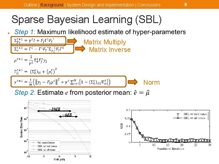
Outline | Background | System Design and Implementation | Conclusions Sparse Bayesian Learning (SBL) • Matrix Multiply Matrix Inverse Norm ~10 d. B ~6 d. B 5

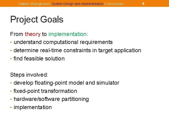
Outline | Background | System Design and Implementation | Conclusions Project Goals From theory to implementation: • understand computational requirements • determine real-time constraints in target application • find feasible solution Steps involved: • develop floating-point model and simulator • fixed-point transformation • hardware/software partitioning • implementation 6

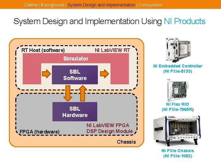
Outline | Background | System Design and Implementation | Conclusions System Design and Implementation Using NI Products RT Host (software) NI Lab. VIEW RT Simulator NI Embedded Controller (NI PXIe-8133) SBL Software NI Flex RIO (NI PXIe-7965 R) SBL Hardware FPGA (hardware) NI Lab. VIEW FPGA DSP Design Module Chassis NI PXIe Chassis (NI PXIe-1082)

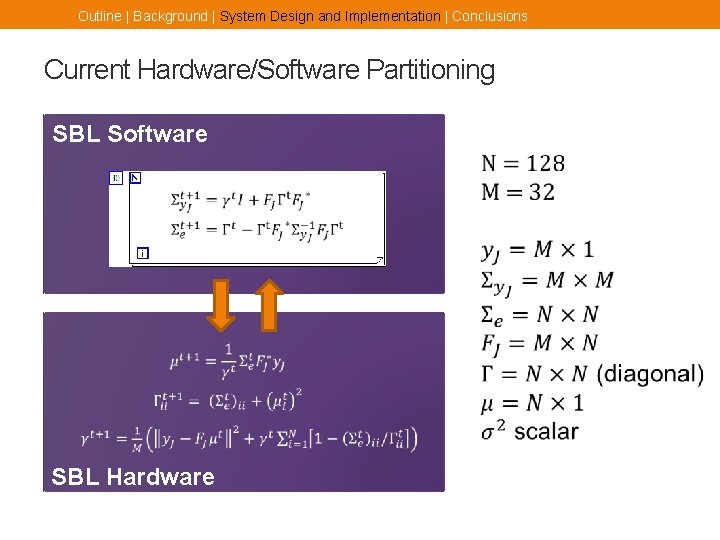
Outline | Background | System Design and Implementation | Conclusions Current Hardware/Software Partitioning SBL Software SBL Hardware

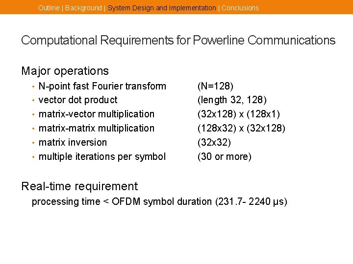
Outline | Background | System Design and Implementation | Conclusions Computational Requirements for Powerline Communications Major operations • N-point fast Fourier transform • vector dot product • matrix-vector multiplication • matrix-matrix multiplication • matrix inversion • multiple iterations per symbol (N=128) (length 32, 128) (32 x 128) x (128 x 1) (128 x 32) x (32 x 128) (32 x 32) (30 or more) Real-time requirement processing time < OFDM symbol duration (231. 7 - 2240 µs)

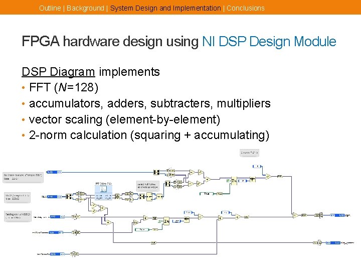
Outline | Background | System Design and Implementation | Conclusions FPGA hardware design using NI DSP Design Module DSP Diagram implements • FFT (N=128) • accumulators, adders, subtracters, multipliers • vector scaling (element-by-element) • 2 -norm calculation (squaring + accumulating)

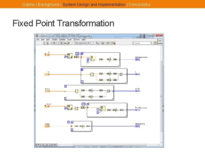
Outline | Background | System Design and Implementation | Conclusions Fixed Point Transformation

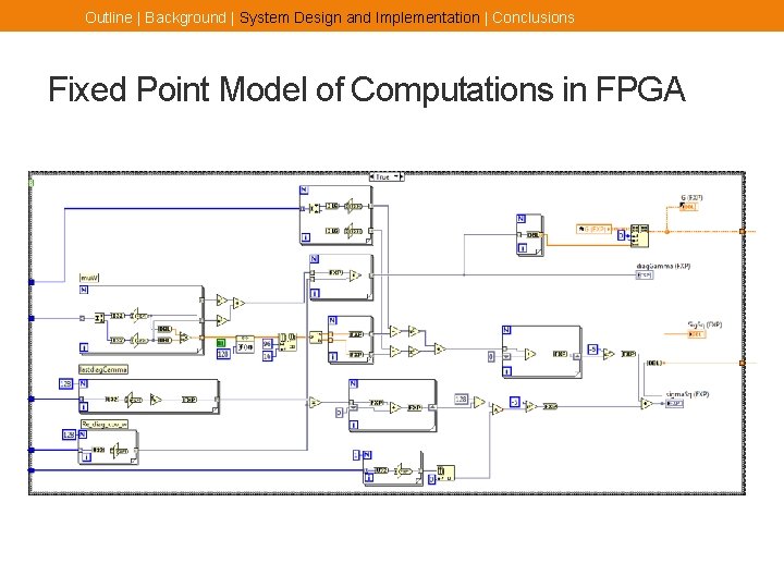
Outline | Background | System Design and Implementation | Conclusions Fixed Point Model of Computations in FPGA

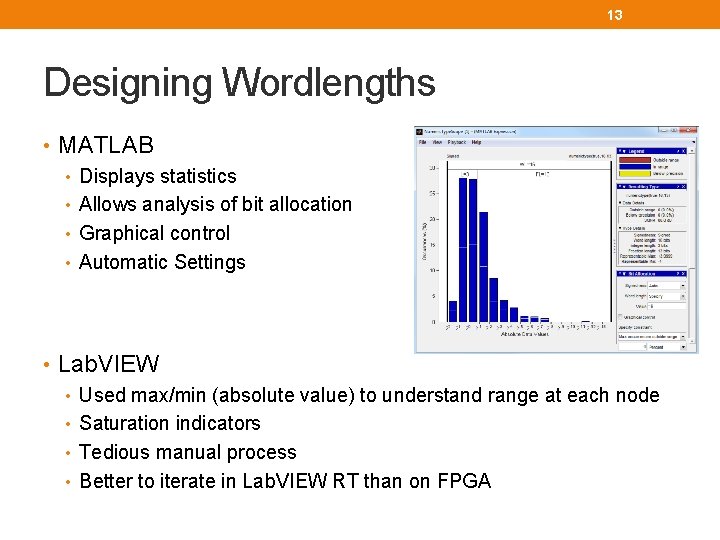
13 Designing Wordlengths • MATLAB • Displays statistics • Allows analysis of bit allocation • Graphical control • Automatic Settings • Lab. VIEW • Used max/min (absolute value) to understand range at each node • Saturation indicators • Tedious manual process • Better to iterate in Lab. VIEW RT than on FPGA

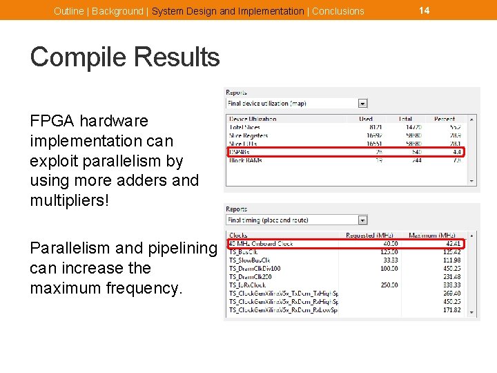
Outline | Background | System Design and Implementation | Conclusions Compile Results FPGA hardware implementation can exploit parallelism by using more adders and multipliers! Parallelism and pipelining can increase the maximum frequency. 14

Outline | Background | System Design and Implementation | Conclusions 15 Advantages of NI DSP Design Module FPGA implementation is greatly simplified! Good level of abstraction to focus on algorithm development and increase productivity, rather than worry about: • clock domains • FIFOs and sizing • handshaking (e. g. data valid, ready for input, output ready, etc. ) • DMA transfers between FPGA and host • etc. Can do a lot with very little/no Lab. VIEW FPGA coding Automatic test bench generation also very useful!

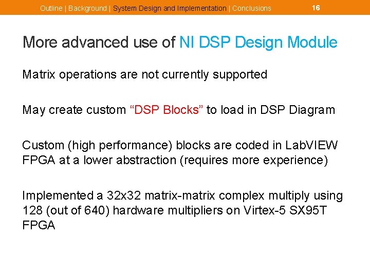
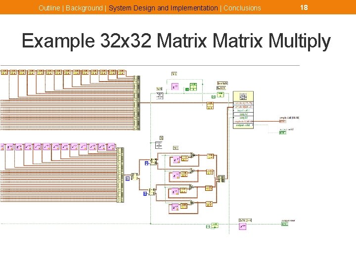
Outline | Background | System Design and Implementation | Conclusions 16 More advanced use of NI DSP Design Module Matrix operations are not currently supported May create custom “DSP Blocks” to load in DSP Diagram Custom (high performance) blocks are coded in Lab. VIEW FPGA at a lower abstraction (requires more experience) Implemented a 32 x 32 matrix-matrix complex multiply using 128 (out of 640) hardware multipliers on Virtex-5 SX 95 T FPGA

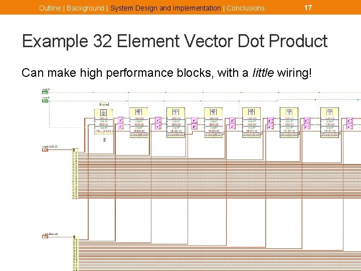
Outline | Background | System Design and Implementation | Conclusions 17 Example 32 Element Vector Dot Product Can make high performance blocks, with a little wiring!

Outline | Background | System Design and Implementation | Conclusions 18 Example 32 x 32 Matrix Multiply

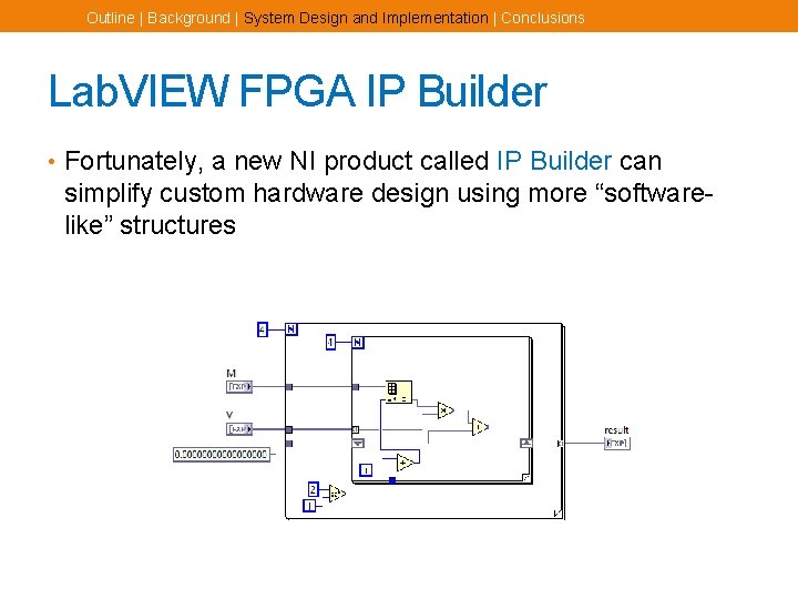
Outline | Background | System Design and Implementation | Conclusions Lab. VIEW FPGA IP Builder • Fortunately, a new NI product called IP Builder can simplify custom hardware design using more “softwarelike” structures

Outline | Background | System Design and Implementation | Conclusions DEMO

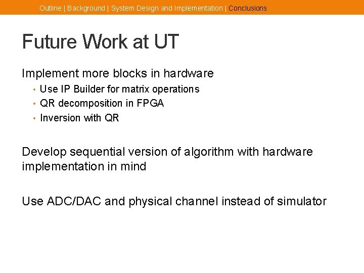
Outline | Background | System Design and Implementation | Conclusions Future Work at UT Implement more blocks in hardware • Use IP Builder for matrix operations • QR decomposition in FPGA • Inversion with QR Develop sequential version of algorithm with hardware implementation in mind Use ADC/DAC and physical channel instead of simulator

22 Thank you for your attention!