FPGA Implementation of a MessagePassing OFDM Receiver for

- Slides: 1

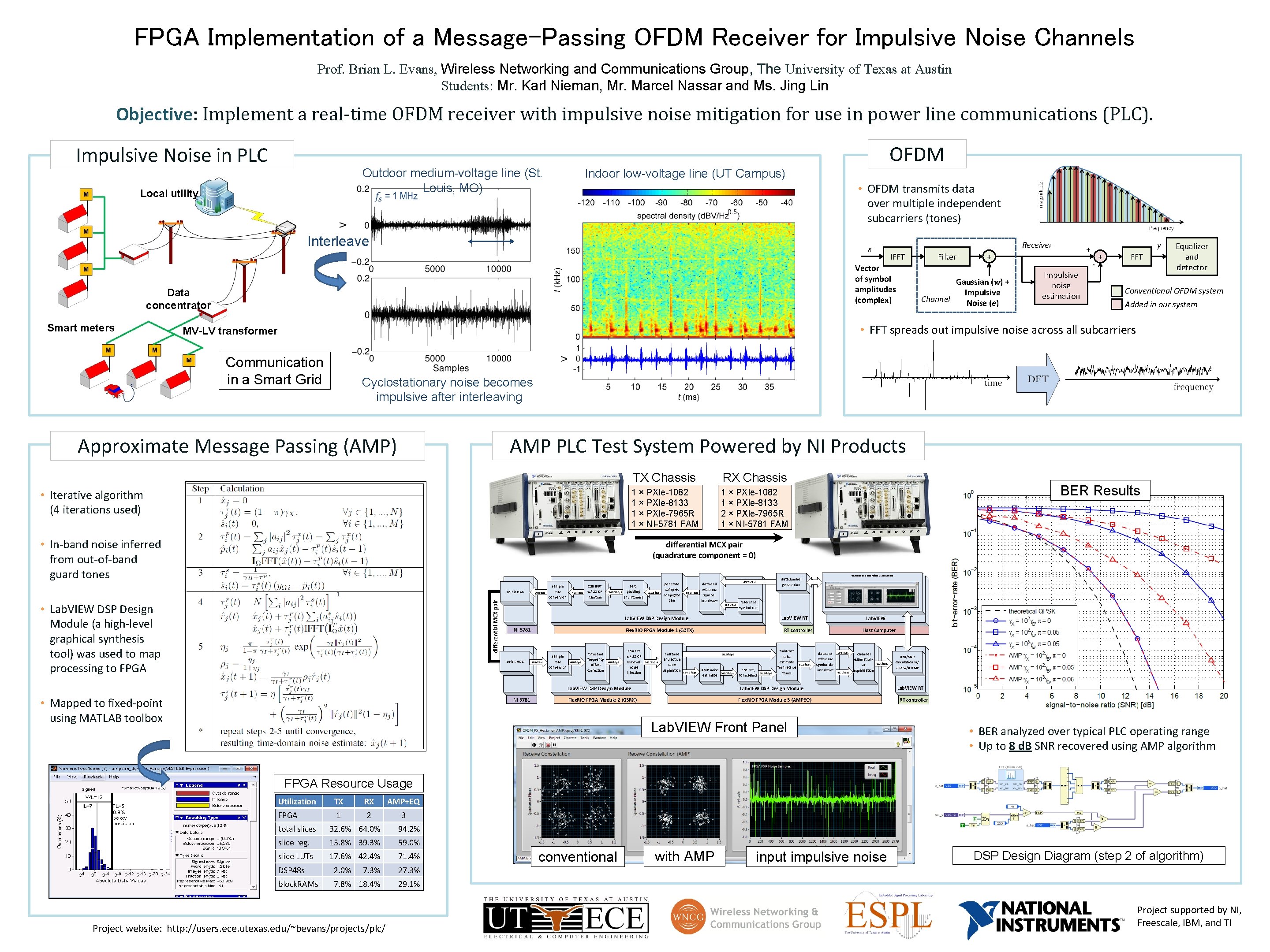
FPGA Implementation of a Message-Passing OFDM Receiver for Impulsive Noise Channels Prof. Brian L. Evans, Wireless Networking and Communications Group, The University of Texas at Austin Students: Mr. Karl Nieman, Mr. Marcel Nassar and Ms. Jing Lin Objective: Implement a real-time OFDM receiver with impulsive noise mitigation for use in power line communications (PLC). Impulsive Noise in PLC OFDM Outdoor medium-voltage line (St. Louis, MO) Local utility Indoor low-voltage line (UT Campus) • OFDM transmits data over multiple independent subcarriers (tones) Interleave IFFT Vector of symbol amplitudes (complex) Data concentrator Smart meters Receiver x Filter + Gaussian (w) + Impulsive Channel Noise (e) y + Impulsive noise estimation - + FFT Equalizer and detector Conventional OFDM system Added in our system • FFT spreads out impulsive noise across all subcarriers MV-LV transformer Communication in a Smart Grid Cyclostationary noise becomes impulsive after interleaving AMP PLC Test System Powered by NI Products Approximate Message Passing (AMP) • Iterative algorithm (4 iterations used) TX Chassis RX Chassis 1 × PXIe-1082 1 × PXIe-8133 1 × PXIe-7965 R 1 × NI-5781 FAM 1 × PXIe-1082 1 × PXIe-8133 2 × PXIe-7965 R 1 × NI-5781 FAM • In-band noise inferred from out-of-band guard tones BER Results differential MCX pair (quadrature component = 0) differential MCX pair 16 -bit DAC • Lab. VIEW DSP Design Module (a high-level graphical synthesis tool) was used to map processing to FPGA 10 MSps sample rate conversion 400 k. Sps 256 IFFT w/ 22 CP insertion 368. 3 k. Sps zero padding (null tones) 103. 6 k. Sps generate complex conjugate pair 51. 8 k. Sps 8. 6 k. Sps reference symbol LUT Lab. VIEW RT Lab. VIEW DSP Design Module NI 5781 14 -bit ADC Flex. RIO FPGA Module 1 (G 3 TX) 10 MSps sample rate conversion 400 k. Sps time and frequency offset correction 400 k. Sps 256 FFT w/ 22 CP removal, noise injection 368. 3 k. Sps null tone and active tone separation 51. 8 k. Sps 184. 2 k. Sps NI 5781 Lab. VIEW RT controller AMP noise estimate 368. 3 k. Sps 256 FFT, tone select 51. 8 k. Sps Subtract noise estimate from active tones 51. 8 k. Sps Host Computer data and reference symbol deinterleave 8. 6 k. Sps 43. 1 k. Sps channel estimation/ ZF equalization 43. 1 k. Sps Lab. VIEW DSP Design Module • Mapped to fixed-point using MATLAB toolbox 43. 2 k. Sps data and reference symbol interleave testbench control/data visualization data symbol generation Flex. RIO FPGA Module 2 (G 3 RX) Flex. RIO FPGA Module 3 (AMPEQ) Lab. VIEW Front Panel BER/SNR calculation w/ and w/o AMP Lab. VIEW RT RT controller • BER analyzed over typical PLC operating range • Up to 8 d. B SNR recovered using AMP algorithm FPGA Resource Usage Utilization TX RX AMP+EQ FPGA 1 2 3 total slices 32. 6% 64. 0% 94. 2% slice reg. 15. 8% 39. 3% 59. 0% slice LUTs 17. 6% 42. 4% 71. 4% DSP 48 s 2. 0% 7. 3% 27. 3% block. RAMs 7. 8% 18. 4% 29. 1% Project website: http: //users. ece. utexas. edu/~bevans/projects/plc/ conventional with AMP input impulsive noise DSP Design Diagram (step 2 of algorithm) Project supported by NI, Freescale, IBM, and TI