FPGA Implementation of a MessagePassing OFDM Receiver for
- Slides: 17

FPGA Implementation of a Message-Passing OFDM Receiver for Impulsive Noise Channels Prof. Brian L. Evans Ph. D Students Karl Nieman, Marcel Nassar, and Jing Lin Department of Electrical and Computer Engineering The University of Texas at Austin, TX May 6, 2013 Sponsored by National Instruments Academic Lead User Program

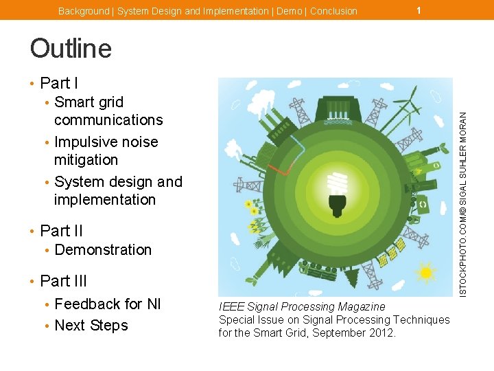
Background | System Design and Implementation | Demo | Conclusion 1 Outline • Part I • Smart grid ISTOCKPHOTO. COM/© SIGAL SUHLER MORAN communications • Impulsive noise mitigation • System design and implementation • Part II • Demonstration • Part III • Feedback for NI • Next Steps IEEE Signal Processing Magazine Special Issue on Signal Processing Techniques for the Smart Grid, September 2012.

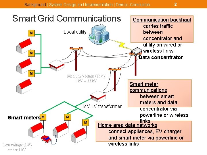
Background | System Design and Implementation | Demo | Conclusion Smart Grid Communications Local utility Medium Voltage (MV) 1 k. V – 33 k. V Smart meters Low voltage (LV) under 1 k. V 2 Communication backhaul carries traffic between concentrator and utility on wired or wireless links Data concentrator Smart meter communications between smart meters and data MV-LV transformer concentrator via powerline or wireless links Home area data networks connect appliances, EV charger and smart meter via powerline or wireless links

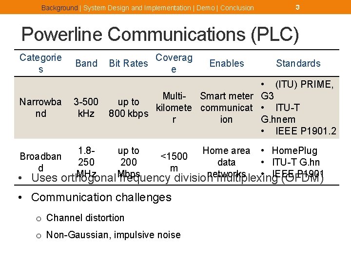
Background | System Design and Implementation | Demo | Conclusion 3 Powerline Communications (PLC) Categorie s Narrowba nd Coverag e Band Bit Rates 3 -500 k. Hz • (ITU) PRIME, Multi- Smart meter G 3 up to kilomete communicat • ITU-T 800 kbps r ion G. hnem • IEEE P 1901. 2 Standards 1. 8 up to Home area • Home. Plug <1500 250 200 data • ITU-T G. hn m MHz Mbps networks • IEEE P 1901 orthogonal frequency division multiplexing (OFDM) Broadban d • Uses Enables • Communication challenges o Channel distortion o Non-Gaussian, impulsive noise

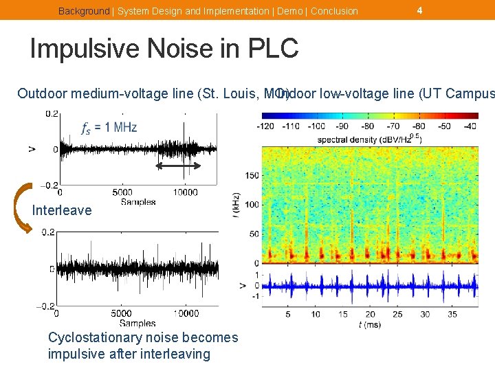
Background | System Design and Implementation | Demo | Conclusion 4 Impulsive Noise in PLC Outdoor medium-voltage line (St. Louis, MO) Indoor low-voltage line (UT Campus Interleave Cyclostationary noise becomes impulsive after interleaving

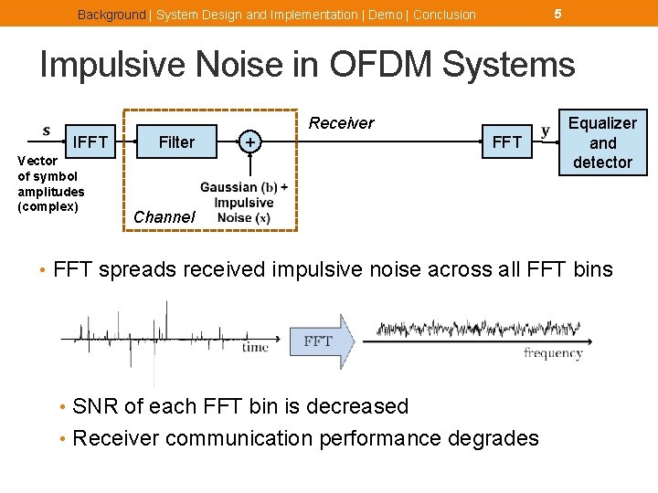
5 Background | System Design and Implementation | Demo | Conclusion Impulsive Noise in OFDM Systems Receiver IFFT Vector of symbol amplitudes (complex) Filter + FFT Equalizer and detector Channel • FFT spreads received impulsive noise across all FFT bins • SNR of each FFT bin is decreased • Receiver communication performance degrades

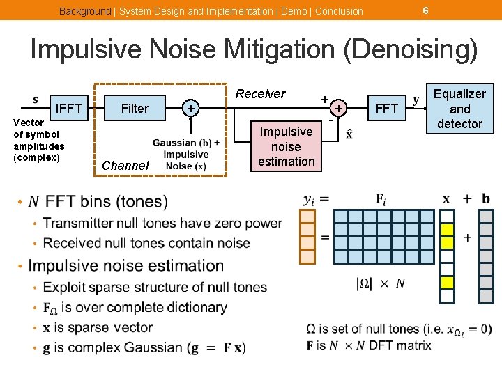
6 Background | System Design and Implementation | Demo | Conclusion Impulsive Noise Mitigation (Denoising) Receiver IFFT Vector of symbol amplitudes (complex) • Filter Channel + Impulsive noise estimation + - + FFT Equalizer and detector

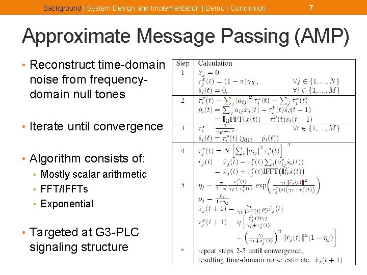
Background | System Design and Implementation | Demo | Conclusion 7 Approximate Message Passing (AMP) • Reconstruct time-domain noise from frequencydomain null tones • Iterate until convergence • Algorithm consists of: • Mostly scalar arithmetic • FFT/IFFTs • Exponential • Targeted at G 3 -PLC signaling structure

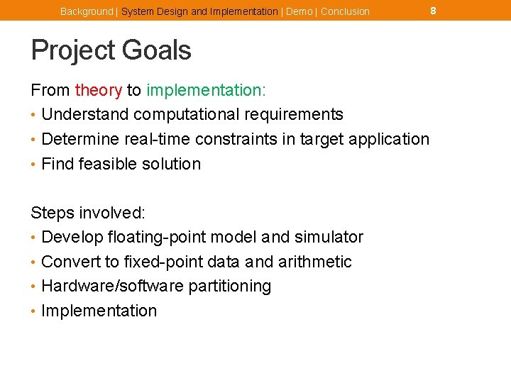
Background | System Design and Implementation | Demo | Conclusion Project Goals From theory to implementation: • Understand computational requirements • Determine real-time constraints in target application • Find feasible solution Steps involved: • Develop floating-point model and simulator • Convert to fixed-point data and arithmetic • Hardware/software partitioning • Implementation 8

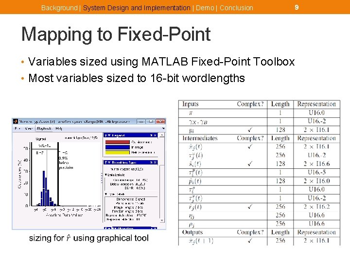
Background | System Design and Implementation | Demo | Conclusion Mapping to Fixed-Point • Variables sized using MATLAB Fixed-Point Toolbox • Most variables sized to 16 -bit wordlengths 9

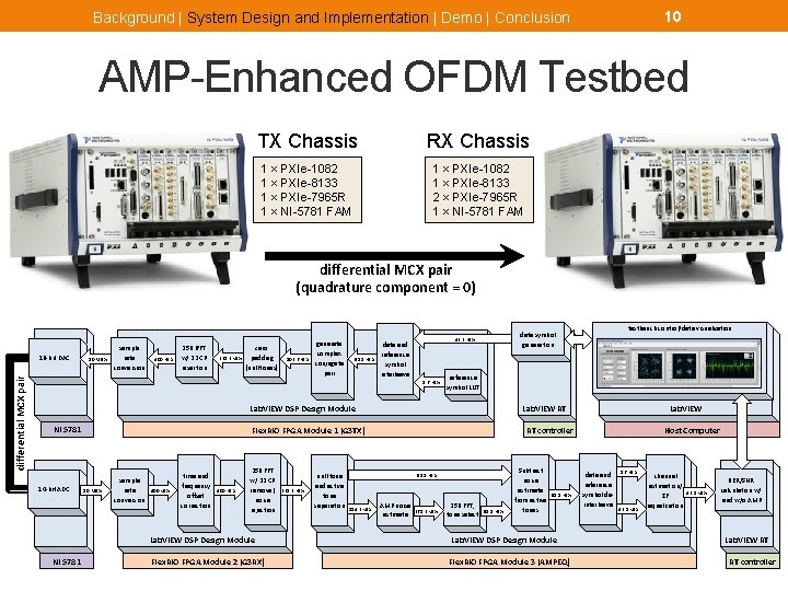
10 Background | System Design and Implementation | Demo | Conclusion AMP-Enhanced OFDM Testbed TX Chassis RX Chassis 1 × PXIe-1082 1 × PXIe-8133 1 × PXIe-7965 R 1 × NI-5781 FAM 1 × PXIe-1082 1 × PXIe-8133 2 × PXIe-7965 R 1 × NI-5781 FAM differential MCX pair (quadrature component = 0) differential MCX pair 16 -bit DAC 10 MSps sample rate conversion 400 k. Sps 256 IFFT w/ 22 CP insertion 368. 3 k. Sps zero padding (null tones) 103. 6 k. Sps generate complex conjugate pair 51. 8 k. Sps data and reference symbol interleave 8. 6 k. Sps reference symbol LUT Lab. VIEW RT Lab. VIEW DSP Design Module NI 5781 14 -bit ADC NI 5781 Flex. RIO FPGA Module 1 (G 3 TX) 10 MSps sample rate conversion 400 k. Sps time and frequency offset correction 400 k. Sps 256 FFT w/ 22 CP removal, noise injection 368. 3 k. Sps null tone and active tone separation Lab. VIEW RT controller 51. 8 k. Sps 184. 2 k. Sps testbench control/data visualization data symbol generation 43. 2 k. Sps AMP noise estimate 368. 3 k. Sps 256 FFT, tone select 51. 8 k. Sps Subtract noise estimate from active tones 51. 8 k. Sps Lab. VIEW DSP Design Module Flex. RIO FPGA Module 2 (G 3 RX) Flex. RIO FPGA Module 3 (AMPEQ) Host Computer data and reference symbol deinterleave 8. 6 k. Sps 43. 1 k. Sps channel estimation/ ZF equalization 43. 1 k. Sps BER/SNR calculation w/ and w/o AMP Lab. VIEW RT RT controller

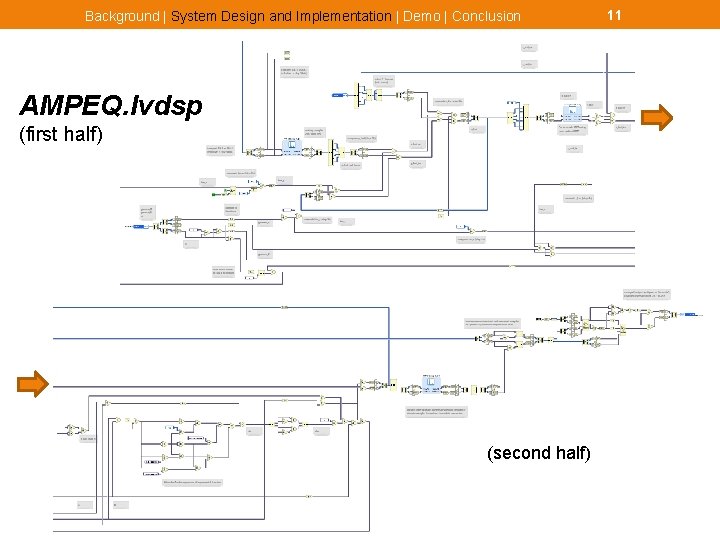
Background | System Design and Implementation | Demo | Conclusion AMPEQ. lvdsp (first half) (second half) 11

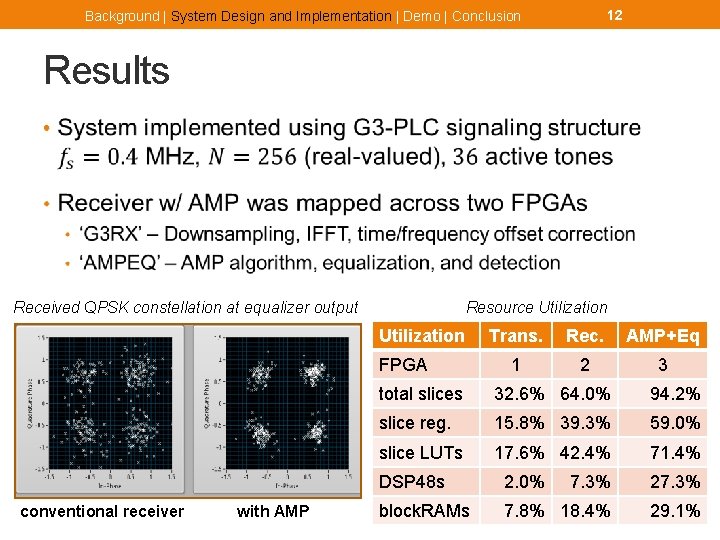
12 Background | System Design and Implementation | Demo | Conclusion Results • Received QPSK constellation at equalizer output Resource Utilization FPGA conventional receiver with AMP Trans. Rec. AMP+Eq 1 2 3 total slices 32. 6% 64. 0% 94. 2% slice reg. 15. 8% 39. 3% 59. 0% slice LUTs 17. 6% 42. 4% 71. 4% DSP 48 s 2. 0% 7. 3% 27. 3% block. RAMs 7. 8% 18. 4% 29. 1%

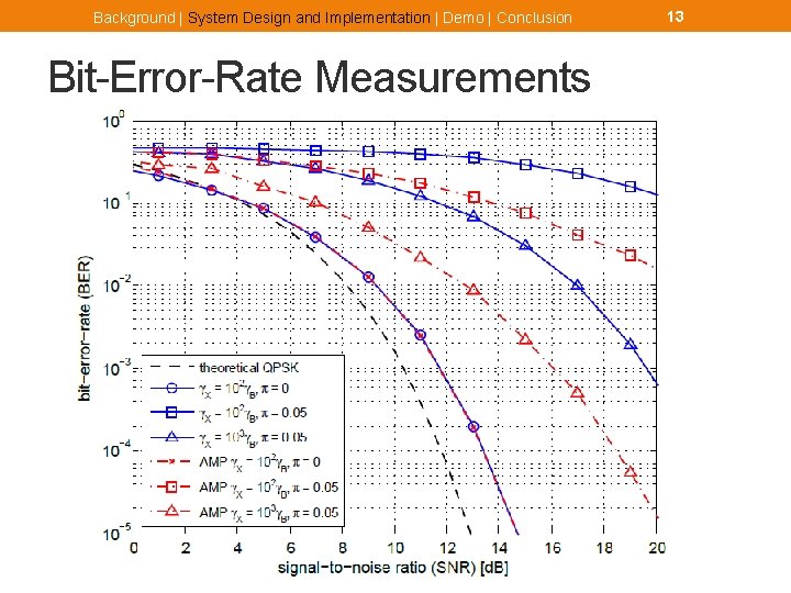
Background | System Design and Implementation | Demo | Conclusion Bit-Error-Rate Measurements 13

Background | System Design and Implementation | Demo | Conclusion DEMO

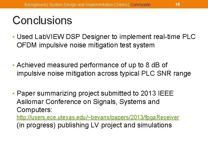
Background | System Design and Implementation | Demo | Conclusion 15 Conclusions • Used Lab. VIEW DSP Designer to implement real-time PLC OFDM impulsive noise mitigation test system • Achieved measured performance of up to 8 d. B of impulsive noise mitigation across typical PLC SNR range • Paper summarizing project submitted to 2013 IEEE Asilomar Conference on Signals, Systems and Computers: http: //users. ece. utexas. edu/~bevans/papers/2013/fpga. Receiver (in progress) publishing LV project and simulations

Background | System Design and Implementation | Demo | Conclusion Thank you for your attention! 16