FPGA for Dummies Design flow ESS FPGA for


- Slides: 22

FPGA for Dummies Design flow ESS | FPGA for Dummies | 2016 -09 -20 | Maurizio Donna

FPGA for Dummies • FPGA Architecture: Ø basic blocks (Logic, FFs, wires and IOs); Ø additional modern elements; • FPGA Programming: ØHDL languages; ØDesign flow; • FPGA DSP: ØArithmetic, FFT and filters; ESS | FPGA for Dummies | 2016 -09 -20 | Maurizio Donna

FPGA for Dummies • FPGA Architecture: Ø basic blocks (Logic, FFs, wires and IOs); Ø additional modern elements; • FPGA Programming: ØHDL languages; ØDesign flow; • FPGA DSP: ØArithmetic, FFT and filters; ESS | FPGA for Dummies | 2016 -09 -20 | Maurizio Donna

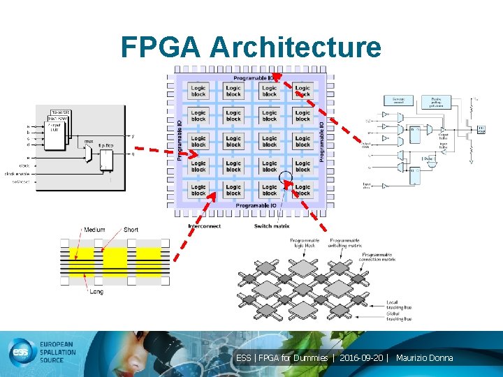
FPGA Architecture ESS | FPGA for Dummies | 2016 -09 -20 | Maurizio Donna

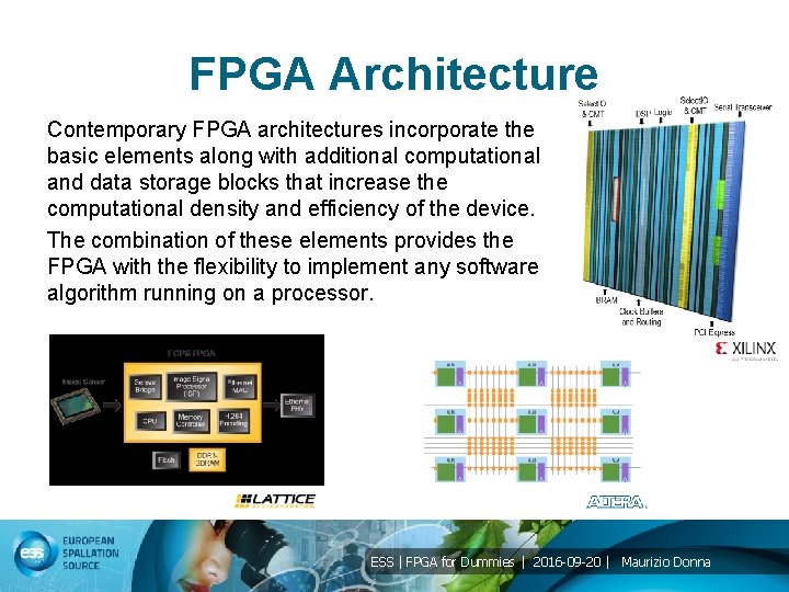
FPGA Architecture Contemporary FPGA architectures incorporate the basic elements along with additional computational and data storage blocks that increase the computational density and efficiency of the device. The combination of these elements provides the FPGA with the flexibility to implement any software algorithm running on a processor. ESS | FPGA for Dummies | 2016 -09 -20 | Maurizio Donna

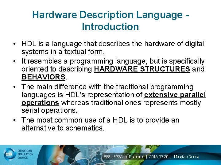
Hardware Description Language Introduction • HDL is a language that describes the hardware of digital systems in a textual form. • It resembles a programming language, but is specifically oriented to describing HARDWARE STRUCTURES and BEHAVIORS. • The main difference with the traditional programming languages is HDL’s representation of extensive parallel operations whereas traditional ones represents mostly serial operations. • The most common use of a HDL is to provide an alternative to schematics. ESS | FPGA for Dummies | 2016 -09 -20 | Maurizio Donna

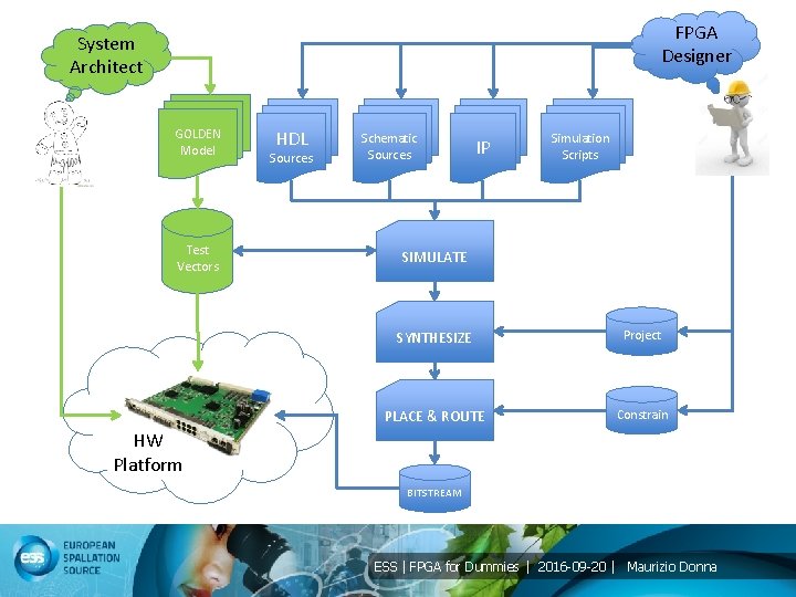
FPGA Designer System Architect GOLDEN Model Test Vectors HDL Sources Schematic Sources IP Simulation Scripts SIMULATE SYNTHESIZE Project PLACE & ROUTE Constrain HW Platform BITSTREAM ESS | FPGA for Dummies | 2016 -09 -20 | Maurizio Donna

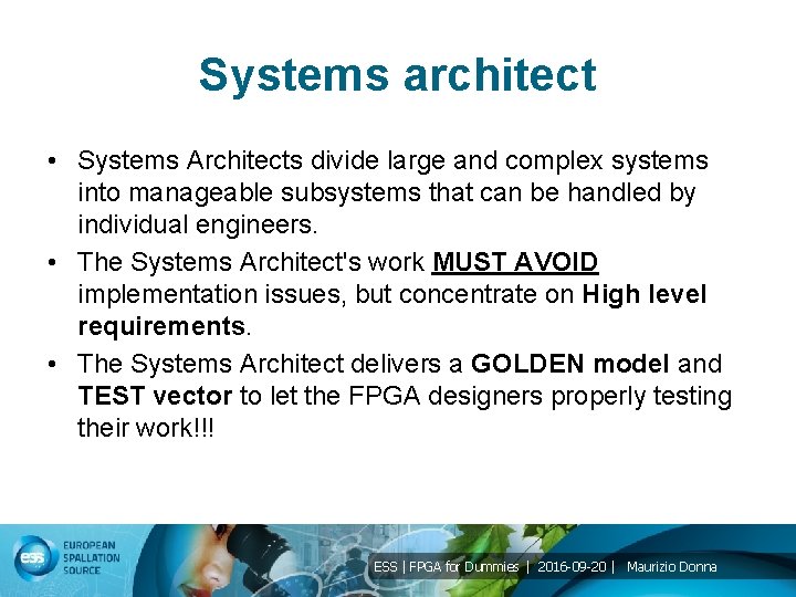
Systems architect • Systems Architects divide large and complex systems into manageable subsystems that can be handled by individual engineers. • The Systems Architect's work MUST AVOID implementation issues, but concentrate on High level requirements. • The Systems Architect delivers a GOLDEN model and TEST vector to let the FPGA designers properly testing their work!!! ESS | FPGA for Dummies | 2016 -09 -20 | Maurizio Donna

FPGA Designer • The FPGA Designer is responsible to deliver a firmware that respect with a good approximation the high level model provided by the SA, on a real HW platform. • The FPGA Designer uses tools to SIMULATE, SYNTHESIZE, PLACE&ROUTE and DOWNLOAD, the FIRMWARE on the FPGA, and verify that the design woks as requested. • Any FPGA provider has is own tools: – XILINX: ISE, EDK, Plan. Ahead, Vivado, etc…. – ALTERA: Quartus, etc… • For SIMULATION and SYNTHESIZE there also Third party tools ESS | FPGA for Dummies | 2016 -09 -20 | Maurizio Donna

Design Entry As a designer create files and add them to your project (FPGA vendor specific), including a user constraints file. • Add any existing files to your project. • Assign constraints such as Ø timing constraints, Ø pin assignments, Ø area constraints. ESS | FPGA for Dummies | 2016 -09 -20 | Maurizio Donna

Functional Verification • You can verify the functionality of your design at different points in the design flow as follows: Ø Before synthesis, run behavioral simulation (also known as Register Transfer Level simulation); Ø After Translate, run functional simulation (also known as gate-level simulation), using the specific vendor library; Ø After device programming, run in-circuit verification. ESS | FPGA for Dummies | 2016 -09 -20 | Maurizio Donna

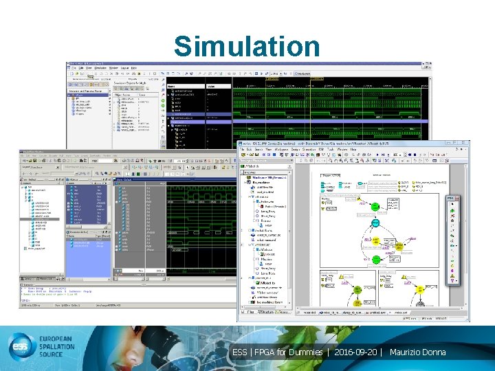
Simulation ESS | FPGA for Dummies | 2016 -09 -20 | Maurizio Donna

Simulation • HDL simulators are software packages that compile and simulate any HDL code (VHDL or/and Verilog, Schematic entry, Thrid part propietary Ips, etc…. ). • FPGA simulation can be performed Ø at an earlier stage to test the Behavior of the HDL code, and fix the algorithm function, as much as close to the provided model; Ø or after the technology P&R using specific vendor library, to verify the firmware without using the HW platform. • this tools support scripting languages (tlc, phyton, etc. . ) to improve the coverage of the testing; • It is necessary to write some additional HDL files (called Test. Benches) to use provided test vector and emulate the interface to the real HW. ESS | FPGA for Dummies | 2016 -09 -20 | Maurizio Donna

Design Synthesis • Logic synthesis is a process by which an abstract form of desired circuit behavior, typically RTL, is turned into a design implementation in terms of logic gates; Ø Logic optimization. Performs two-level or multi-level minimization of the Boolean equations to optimize area, delay, or a combination of both; ESS | FPGA for Dummies | 2016 -09 -20 | Maurizio Donna

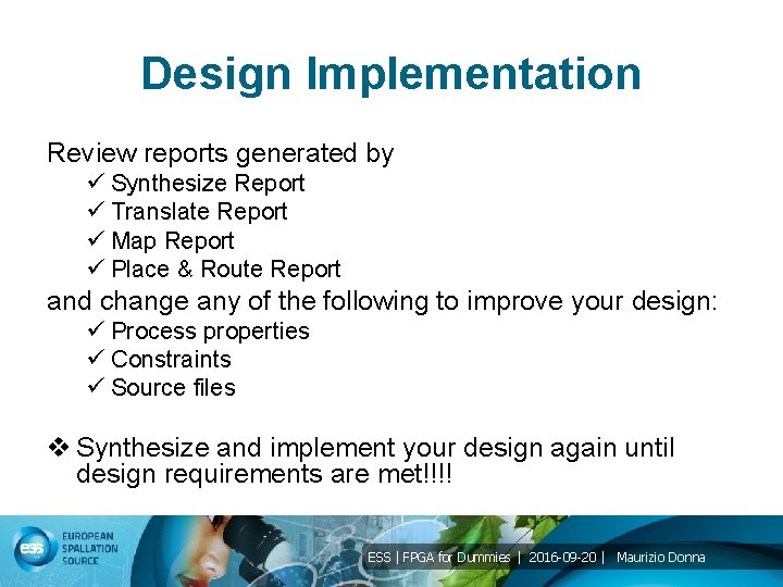
Design Implementation of a design includes the following steps: Ø Translate to vendor specific library of technology components; Ø Map: Transforms the Boolean equations into a circuit of FPGA logic blocks. This step also optimizes Øthe total number of logic blocks required (area optimization) Øthe number of logic blocks in time-critical paths (delay optimization). ESS | FPGA for Dummies | 2016 -09 -20 | Maurizio Donna

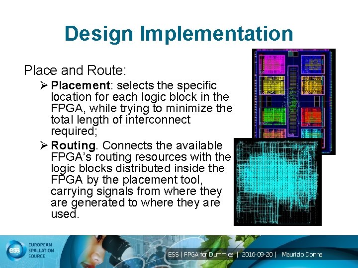
Design Implementation Place and Route: Ø Placement: selects the specific location for each logic block in the FPGA, while trying to minimize the total length of interconnect required; Ø Routing. Connects the available FPGA’s routing resources with the logic blocks distributed inside the FPGA by the placement tool, carrying signals from where they are generated to where they are used. ESS | FPGA for Dummies | 2016 -09 -20 | Maurizio Donna

Design Implementation Review reports generated by ü Synthesize Report ü Translate Report ü Map Report ü Place & Route Report and change any of the following to improve your design: ü Process properties ü Constraints ü Source files v Synthesize and implement your design again until design requirements are met!!!! ESS | FPGA for Dummies | 2016 -09 -20 | Maurizio Donna

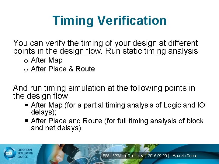
Timing Verification You can verify the timing of your design at different points in the design flow. Run static timing analysis o After Map o After Place & Route And run timing simulation at the following points in the design flow: After Map (for a partial timing analysis of Logic and IO delays); After Place and Route (for full timing analysis of block and net delays). ESS | FPGA for Dummies | 2016 -09 -20 | Maurizio Donna

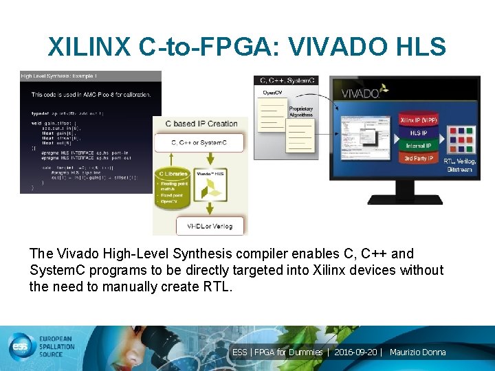
XILINX C-to-FPGA: VIVADO HLS The Vivado High-Level Synthesis compiler enables C, C++ and System. C programs to be directly targeted into Xilinx devices without the need to manually create RTL. ESS | FPGA for Dummies | 2016 -09 -20 | Maurizio Donna

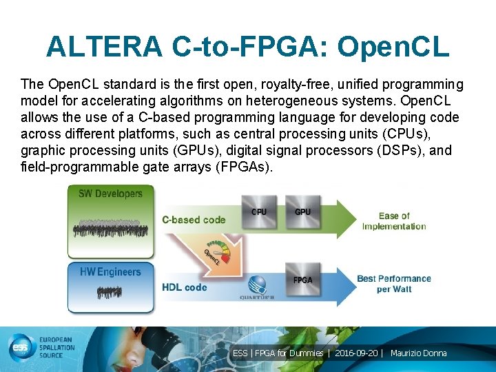
ALTERA C-to-FPGA: Open. CL The Open. CL standard is the first open, royalty-free, unified programming model for accelerating algorithms on heterogeneous systems. Open. CL allows the use of a C-based programming language for developing code across different platforms, such as central processing units (CPUs), graphic processing units (GPUs), digital signal processors (DSPs), and field-programmable gate arrays (FPGAs). ESS | FPGA for Dummies | 2016 -09 -20 | Maurizio Donna

Questions ESS | FPGA for Dummies | 2016 -09 -20 | Maurizio Donna

ESS | FPGA for Dummies | 2016 -09 -20 | Maurizio Donna