CSE 301 Microprocessors Dr Md Sujan Ali Associate
![Register structure of 8086 (cont’d) ü Segment Register [N. B. Please see BIU] 08 Register structure of 8086 (cont’d) ü Segment Register [N. B. Please see BIU] 08](https://slidetodoc.com/presentation_image_h2/5fc15ab0b86f7a45b8a97989cc45fd53/image-29.jpg)
![Direct Data Addressing Figure 4 The operation of the MOV AL, [1234 H] instruction Direct Data Addressing Figure 4 The operation of the MOV AL, [1234 H] instruction](https://slidetodoc.com/presentation_image_h2/5fc15ab0b86f7a45b8a97989cc45fd53/image-52.jpg)
![Register Indirect Addressing Figure 5 The operation of the MOV AX, [BX] instruction when Register Indirect Addressing Figure 5 The operation of the MOV AX, [BX] instruction when](https://slidetodoc.com/presentation_image_h2/5fc15ab0b86f7a45b8a97989cc45fd53/image-54.jpg)
![Register Relative Addressing Figure 7 The operation of the MOV AX, [BX=1000 H] instructon, Register Relative Addressing Figure 7 The operation of the MOV AX, [BX=1000 H] instructon,](https://slidetodoc.com/presentation_image_h2/5fc15ab0b86f7a45b8a97989cc45fd53/image-59.jpg)
- Slides: 83

CSE 301 Microprocessors Dr. Md. Sujan Ali Associate Professor Dept. of Computer Science and Engineering Jatiya Kabi Kazi Nazrul Islam University Trishal, Mymensingh, Bangladesh

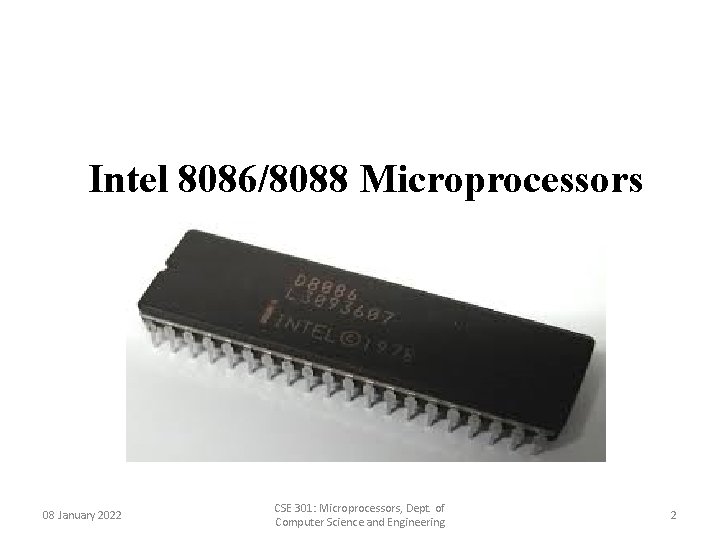
Intel 8086/8088 Microprocessors 08 January 2022 CSE 301: Microprocessors, Dept. of Computer Science and Engineering 2

Intel 8086 microprocessor • The 8086, announced in 1978, was the first 16 -bit microprocessor introduced by Intel Corporation. • 8086 is 16 -bit microprocessor. • 8086 has a 20 bit address bus can access upto 220 memory locations ( 1 MB). • Externally the 8086 has a 16 -bit data bus 8086 has the ability to address up to 1 Mbyte of memory and 64 K of input/output port. • The 8086 is manufactured using high-performance metal -oxide semiconductor (HMOS) technology. • The 8086 is housed in a 40 -pin dual inline package and many pins have multiple functions. 08 January 2022 CSE 301: Microprocessors, Dept. of Computer Science and Engineering 3

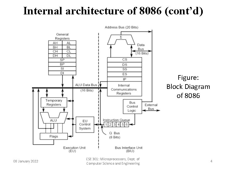
Internal architecture of 8086 (cont’d) Figure: Block Diagram of 8086 08 January 2022 CSE 301: Microprocessors, Dept. of Computer Science and Engineering 4

Internal architecture of 8086 (cont’d) ü The architecture of 8086 includes – Arithmetic Logic Unit (ALU) – Flags – General registers – Instruction byte queue – Segment registers 08 January 2022 CSE 301: Microprocessors, Dept. of Computer Science and Engineering 5

Internal architecture of 8086 (cont’d) ü The 8086 CPU is divided into two independent functional units: o Bus Interface Unit (BIU) • The BIU has to interact with memory and input and output devices in fetching the instructions and data required by the EU o Execution Unit (EU) • EU is responsible for executing the instructions of the programs and to carry out the required processing 08 January 2022 CSE 301: Microprocessors, Dept. of Computer Science and Engineering 6

Internal architecture of 8086 (cont’d) ü Bus Interface Unit (BIU) o The BIU has – Instruction stream byte queue – A set of segment registers – Instruction pointer 08 January 2022 CSE 301: Microprocessors, Dept. of Computer Science and Engineering 7

Internal architecture of 8086 (cont’d) ü BIU – Instruction Byte Queue • 8086 instructions vary from 1 to 6 bytes • Therefore fetch and execution are taking place concurrently in order to improve the performance of the microprocessor • The BIU feeds the instruction stream to the execution unit through a 6 byte prefetch queue • This prefetch queue can be considered as a form of loosely coupled pipelining 08 January 2022 CSE 301: Microprocessors, Dept. of Computer Science and Engineering 8

Internal architecture of 8086 (cont’d) ü BIU – Instruction Byte Queue • Execution and decoding of certain instructions do not require the use of buses • While such instructions are executed, the BIU fetches up to six instruction bytes for the following instructions (the subsequent instructions) • The BIU store these prefetched bytes in a first-in-first out register by name instruction byte queue • When the EU is ready for its next instruction, it simply reads the instruction byte(s) for the instruction from the queue in BIU 08 January 2022 CSE 301: Microprocessors, Dept. of Computer Science and Engineering 9

Internal architecture of 8086 (cont’d) ü Segment Registers (cont’d) • The memory of 8086 is divided into 4 segments namely – Code segment (program memory) – Data segment (data memory) – Stack memory (stack segment) – Extra memory (extra segment) 08 January 2022 CSE 301: Microprocessors, Dept. of Computer Science and Engineering 10

Internal architecture of 8086 (cont’d) ü Segment Registers (cont’d) o Code Segment (CS) register • It is a 16 -bit register containing address of 64 KB segment with processor instructions • The processor uses CS segment for all accesses to instructions referenced by instruction pointer (IP) register • It points to the starting address of the code segment 08 January 2022 CSE 301: Microprocessors, Dept. of Computer Science and Engineering 11

Internal architecture of 8086 (cont’d) ü Segment Registers (cont’d) o Stack Segment (SS) register • It is a 16 -bit register containing address of 64 KB segment with program stack • By default, the processor assumes that all data referenced by the stack pointer (SP) and base pointer (BP) registers is located in the stack segment • It is used to compute the address of the stack location to be accessed. 08 January 2022 CSE 301: Microprocessors, Dept. of Computer Science and Engineering 12

Internal architecture of 8086 (cont’d) ü Segment Registers (cont’d) o Data Segment (DS) register • It is a 16 -bit register containing address of 64 KB segment with program data • By default, the processor assumes that all data referenced by general registers (AX, BX, CX, DX) and index register (SI, DI) is located in the data segment • It points to the starting address of the data segment. The maximum capacity of a segment may be up to 64 Kbytes. The starting address is divisible by 16. 08 January 2022 CSE 301: Microprocessors, Dept. of Computer Science and Engineering 13

Internal architecture of 8086 (cont’d) ü Segment Registers o Extra Segment (ES) register • It is a 16 -bit register containing address of 64 KB segment, usually with program data • By default, the processor assumes that the DI register references the ES segment in string manipulation instructions 08 January 2022 CSE 301: Microprocessors, Dept. of Computer Science and Engineering 14

Internal architecture of 8086 (cont’d) ü Instruction pointer o It points to the address of the next instruction to be executed. 08 January 2022 CSE 301: Microprocessors, Dept. of Computer Science and Engineering 15

Internal architecture of 8086 (cont’d) ü Execution Unit (EU) (cont’d) o The Execution Unit (EU) has – Control unit – Instruction decoder – Arithmetic and Logical Unit (ALU) – General registers – Flag register – Pointers – Index registers 08 January 2022 CSE 301: Microprocessors, Dept. of Computer Science and Engineering 16

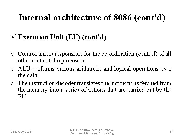
Internal architecture of 8086 (cont’d) ü Execution Unit (EU) (cont’d) o Control unit is responsible for the co-ordination (control) of all other units of the processor o ALU performs various arithmetic and logical operations over the data o The instruction decoder translates the instructions fetched from the memory into a series of actions that are carried out by the EU 08 January 2022 CSE 301: Microprocessors, Dept. of Computer Science and Engineering 17

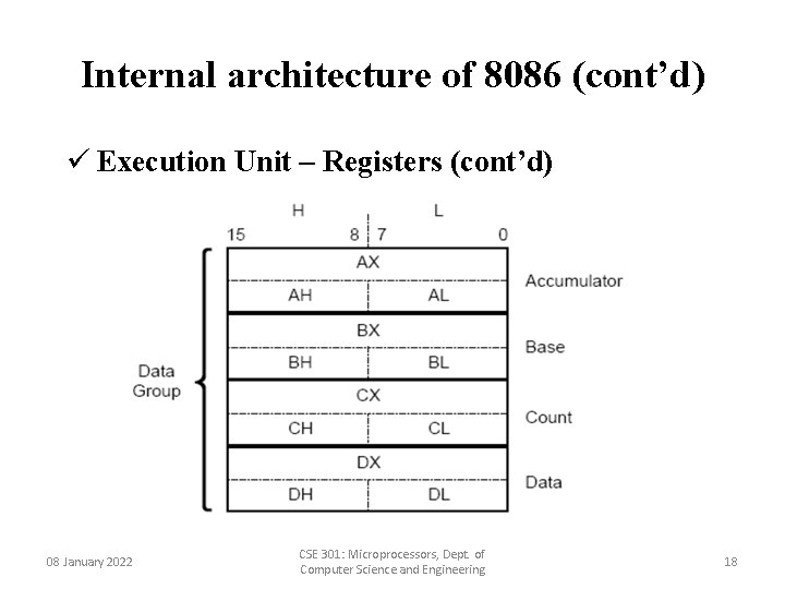
Internal architecture of 8086 (cont’d) ü Execution Unit – Registers (cont’d) 08 January 2022 CSE 301: Microprocessors, Dept. of Computer Science and Engineering 18

Internal architecture of 8086 (cont’d) ü Execution Unit – Registers (cont’d) o General registers are used for temporary storage and manipulation of data and instructions o Accumulator register consists of two 8 -bit registers AL and AH, which can be combined together and used as a 16 -bit register AX o Accumulator can be used for I/O operations and string manipulation 08 January 2022 CSE 301: Microprocessors, Dept. of Computer Science and Engineering 19

Internal architecture of 8086 (cont’d) ü Execution Unit – Registers (cont’d) o Base register consists of two 8 -bit registers BL and BH, which can be combined together and used as a 16 -bit register BX o BX register usually contains a data pointer used for based, based indexed or register indirect addressing o Count register consists of two 8 -bit registers CL and CH, which can be combined together and used as a 16 -bit register CX o Count register can be used as a counter in string manipulation and shift/rotate instructions 08 January 2022 CSE 301: Microprocessors, Dept. of Computer Science and Engineering 20

Internal architecture of 8086 (cont’d) ü Execution Unit – Registers (cont’d) o Data register consists of two 8 -bit registers DL and DH, which can be combined together and used as a 16 -bit register DX o Data register can be used as a port number in I/O operations o In integer 32 -bit multiply and divide instruction the DX register contains high-order word of the initial or resulting number 08 January 2022 CSE 301: Microprocessors, Dept. of Computer Science and Engineering 21

Internal architecture of 8086 (cont’d) ü Execution Unit – Registers o Base register consists of two 8 -bit registers BL and BH, which can be combined together and used as a 16 -bit register BX o BX register usually contains a data pointer used for based, based indexed or register indirect addressing o Count register consists of two 8 -bit registers CL and CH, which can be combined together and used as a 16 -bit register CX o Count register can be used as a counter in string manipulation and shift/rotate instructions 08 January 2022 CSE 301: Microprocessors, Dept. of Computer Science and Engineering 22

Internal architecture of 8086 (cont’d) ü Execution Unit – Functions o The functions of execution unit are: • To tell BIU where to fetch the instructions or data from. • To decode the instructions. • To execute the instructions. • The EU contains the control circuitry to perform various internal operations. • A decoder in EU decodes the instruction fetched memory to generate different internal or external control signals required to perform the operation. • EU has 16 -bit ALU, which can perform arithmetic and logical operations on 8 -bit as well as 16 -bit. 08 January 2022 CSE 301: Microprocessors, Dept. of Computer Science and Engineering 23

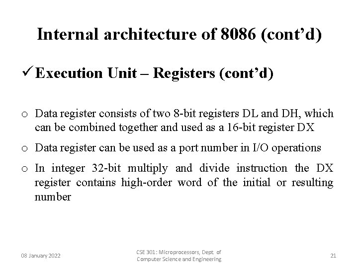
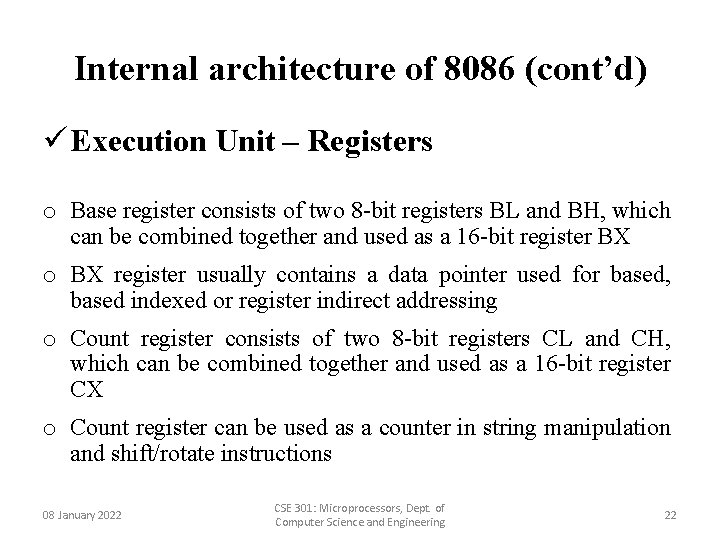
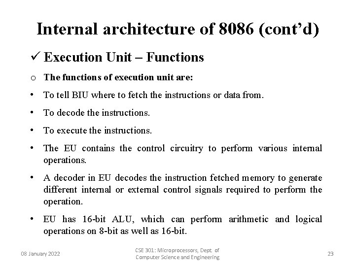
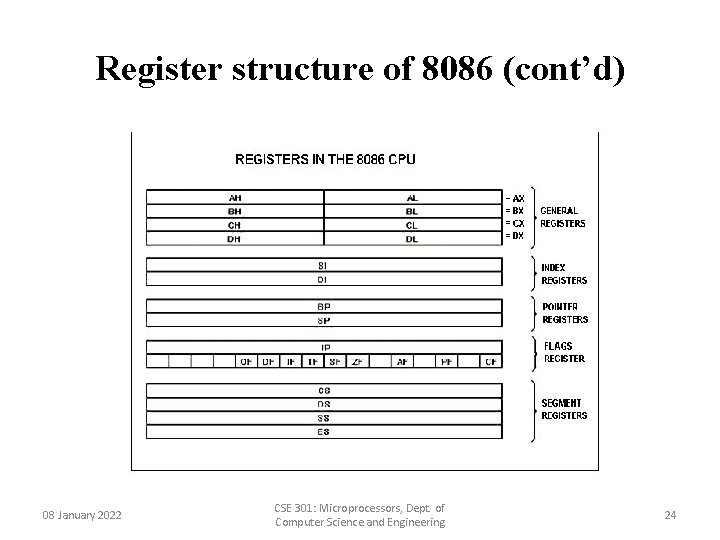
Register structure of 8086 (cont’d) 08 January 2022 CSE 301: Microprocessors, Dept. of Computer Science and Engineering 24

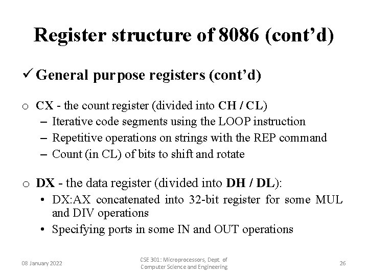
Register structure of 8086 (cont’d) ü General purpose registers (cont’d) q 8086 CPU has 8 general purpose registers o AX - the accumulator register (divided into AH / AL): – – – Generates shortest machine code Arithmetic, logic and data transfer One number must be in AL or AX Multiplication & Division Input & Output o BX - the base address register (divided into BH / BL). 08 January 2022 CSE 301: Microprocessors, Dept. of Computer Science and Engineering 25

Register structure of 8086 (cont’d) ü General purpose registers (cont’d) o CX - the count register (divided into CH / CL) – Iterative code segments using the LOOP instruction – Repetitive operations on strings with the REP command – Count (in CL) of bits to shift and rotate o DX - the data register (divided into DH / DL): • DX: AX concatenated into 32 -bit register for some MUL and DIV operations • Specifying ports in some IN and OUT operations 08 January 2022 CSE 301: Microprocessors, Dept. of Computer Science and Engineering 26

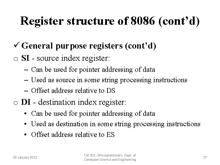
Register structure of 8086 (cont’d) ü General purpose registers (cont’d) o SI - source index register: – Can be used for pointer addressing of data – Used as source in some string processing instructions – Offset address relative to DS o DI - destination index register: • Can be used for pointer addressing of data • Used as destination in some string processing instructions • Offset address relative to ES 08 January 2022 CSE 301: Microprocessors, Dept. of Computer Science and Engineering 27

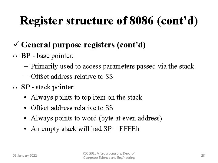
Register structure of 8086 (cont’d) ü General purpose registers (cont’d) o BP - base pointer: – Primarily used to access parameters passed via the stack – Offset address relative to SS o SP - stack pointer: • Always points to top item on the stack • Offset address relative to SS • Always points to word (byte at even address) • An empty stack will had SP = FFFEh 08 January 2022 CSE 301: Microprocessors, Dept. of Computer Science and Engineering 28
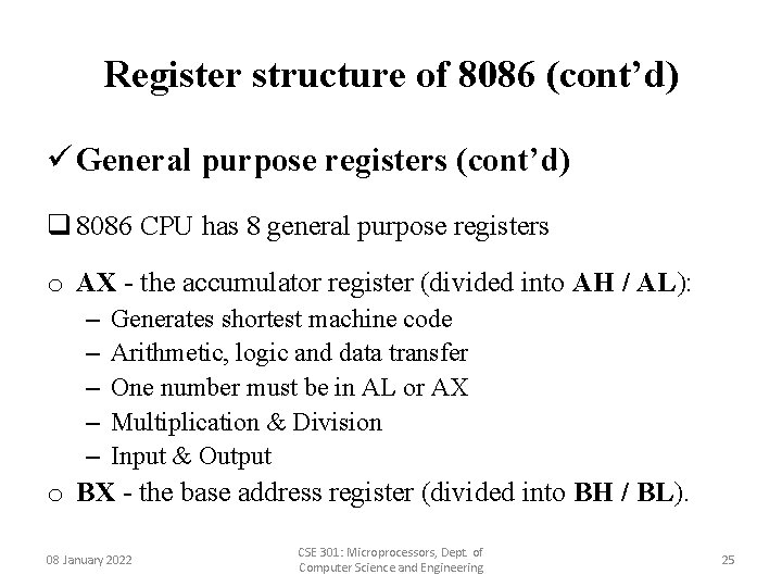
![Register structure of 8086 contd ü Segment Register N B Please see BIU 08 Register structure of 8086 (cont’d) ü Segment Register [N. B. Please see BIU] 08](https://slidetodoc.com/presentation_image_h2/5fc15ab0b86f7a45b8a97989cc45fd53/image-29.jpg)
Register structure of 8086 (cont’d) ü Segment Register [N. B. Please see BIU] 08 January 2022 CSE 301: Microprocessors, Dept. of Computer Science and Engineering 29

Register structure of 8086 (cont’d) ü Special purpose registers (cont’d) o IP - the instruction pointer: – Always points to next instruction to be executed – Offset address relative to CS – IP register always works together with CS segment register and it points to currently executing instruction. o SP - Stack Pointer – SP addresses an area of memory called the stack. – The stack memory is a data LIFO data structure. – The register is referred to as SP if used in 16 bit mode and ESP if referred to as a 32 bit register. 08 January 2022 CSE 301: Microprocessors, Dept. of Computer Science and Engineering 30

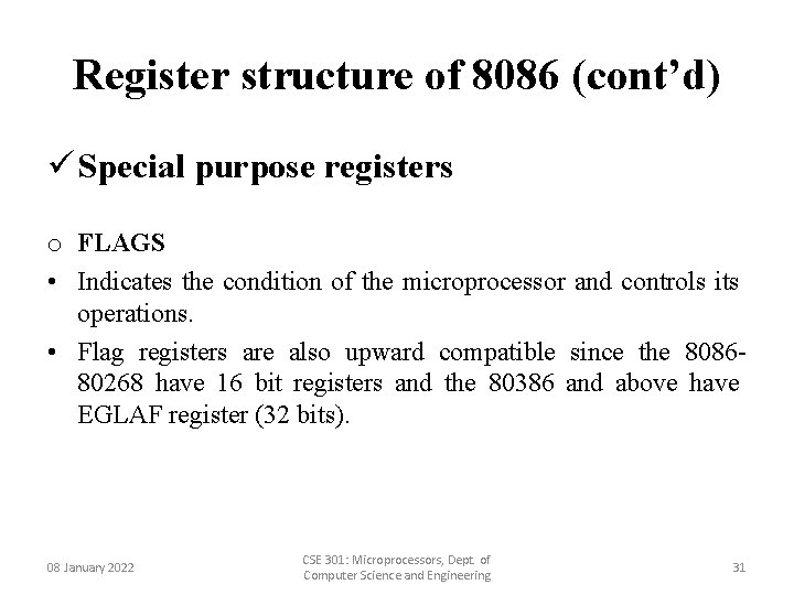
Register structure of 8086 (cont’d) ü Special purpose registers o FLAGS • Indicates the condition of the microprocessor and controls its operations. • Flag registers are also upward compatible since the 808680268 have 16 bit registers and the 80386 and above have EGLAF register (32 bits). 08 January 2022 CSE 301: Microprocessors, Dept. of Computer Science and Engineering 31

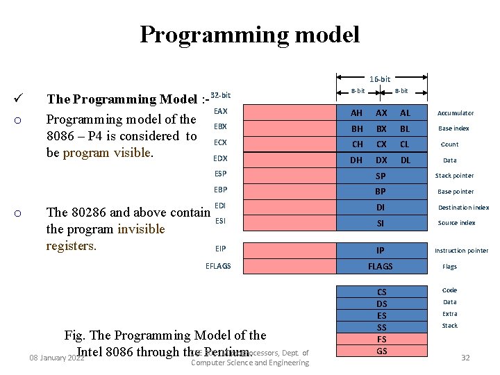
Programming model 16 -bit ü o o 32 -bit The Programming Model : EAX Programming model of the EBX 8086 – P 4 is considered to ECX be program visible. EDX 8 -bit AH AX AL Accumulator BH BX BL Base index CH CX CL Count DH DX DL Data ESP SP Stack pointer EBP BP Base pointer EDI DI Destination index ESI SI Source index EIP IP EFLAGS Flags CS DS ES SS FS GS Code The 80286 and above contain the program invisible registers. Fig. The Programming Model of the CSE Pentium. 301: Microprocessors, Dept. of Intel 8086 through the 08 January 2022 Computer Science and Engineering Instruction pointer Data Extra Stack 32

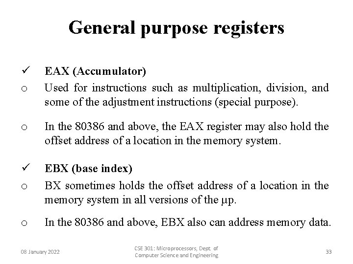
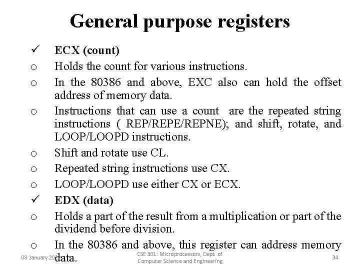
General purpose registers ü o EAX (Accumulator) Used for instructions such as multiplication, division, and some of the adjustment instructions (special purpose). o In the 80386 and above, the EAX register may also hold the offset address of a location in the memory system. ü o EBX (base index) BX sometimes holds the offset address of a location in the memory system in all versions of the µp. o In the 80386 and above, EBX also can address memory data. 08 January 2022 CSE 301: Microprocessors, Dept. of Computer Science and Engineering 33

General purpose registers ü o o ECX (count) Holds the count for various instructions. In the 80386 and above, EXC also can hold the offset address of memory data. o Instructions that can use a count are the repeated string instructions ( REP/REPE/REPNE); and shift, rotate, and LOOP/LOOPD instructions. o Shift and rotate use CL. o Repeated string instructions use CX. o LOOP/LOOPD use either CX or ECX. ü EDX (data) o Holds a part of the result from a multiplication or part of the dividend before division. o In the 80386 and above, this register can address memory CSE 301: Microprocessors, Dept. of 08 January 2022 34 data. Computer Science and Engineering

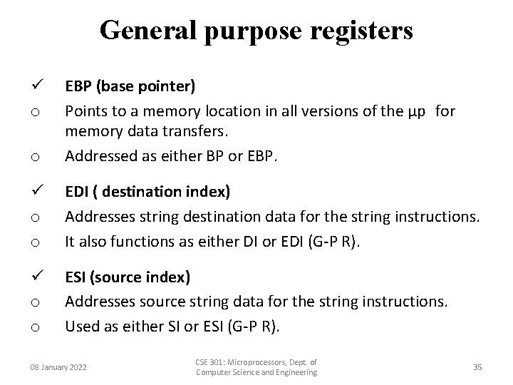
General purpose registers o EBP (base pointer) Points to a memory location in all versions of the µp for memory data transfers. Addressed as either BP or EBP. ü o o EDI ( destination index) Addresses string destination data for the string instructions. It also functions as either DI or EDI (G-P R). ü o o ESI (source index) Addresses source string data for the string instructions. Used as either SI or ESI (G-P R). ü o 08 January 2022 CSE 301: Microprocessors, Dept. of Computer Science and Engineering 35

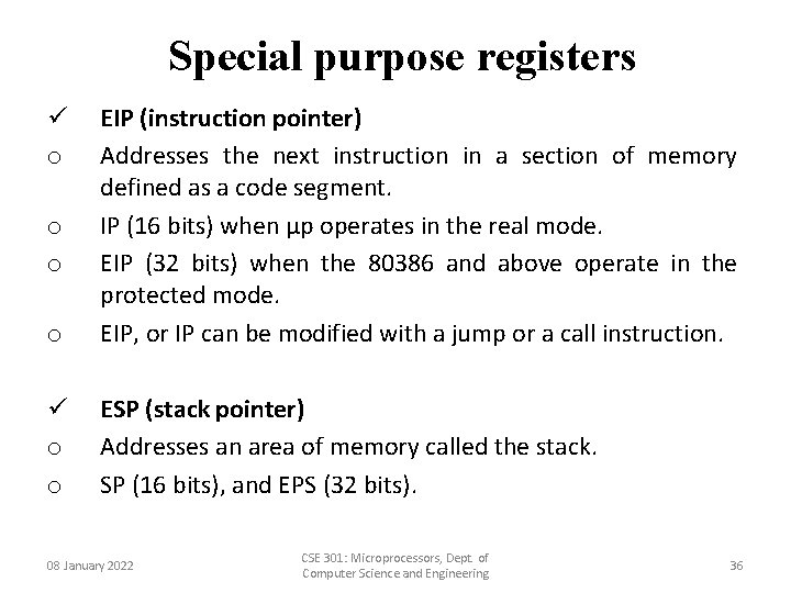
Special purpose registers o EIP (instruction pointer) Addresses the next instruction in a section of memory defined as a code segment. IP (16 bits) when µp operates in the real mode. EIP (32 bits) when the 80386 and above operate in the protected mode. EIP, or IP can be modified with a jump or a call instruction. ü o o ESP (stack pointer) Addresses an area of memory called the stack. SP (16 bits), and EPS (32 bits). ü o o o 08 January 2022 CSE 301: Microprocessors, Dept. of Computer Science and Engineering 36

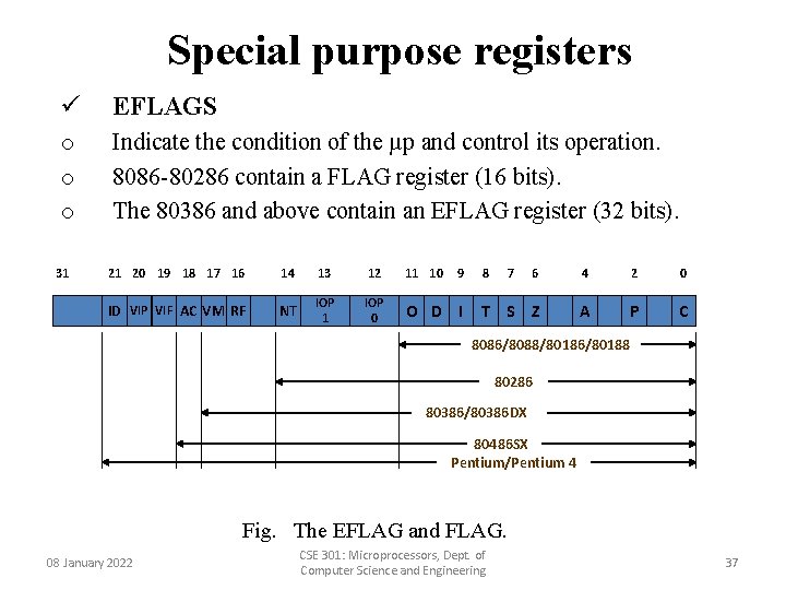
Special purpose registers ü EFLAGS o o o Indicate the condition of the µp and control its operation. 8086 -80286 contain a FLAG register (16 bits). The 80386 and above contain an EFLAG register (32 bits). 31 21 20 19 18 17 16 14 13 12 11 10 9 ID VIP VIF AC VM RF NT IOP 1 IOP 0 O D I 8 7 6 4 2 0 T S Z A P C 8086/8088/80186/80188 80286 80386/80386 DX 80486 SX Pentium/Pentium 4 Fig. The EFLAG and FLAG. 08 January 2022 CSE 301: Microprocessors, Dept. of Computer Science and Engineering 37

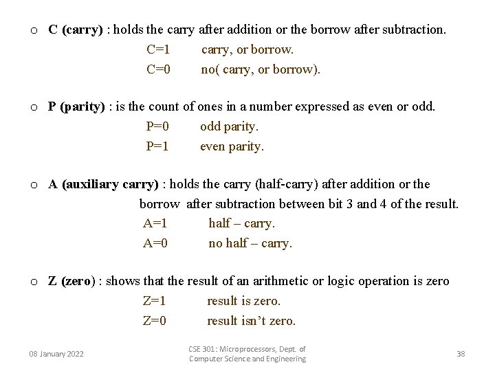
o C (carry) : holds the carry after addition or the borrow after subtraction. C=1 carry, or borrow. C=0 no( carry, or borrow). o P (parity) : is the count of ones in a number expressed as even or odd. P=0 odd parity. P=1 even parity. o A (auxiliary carry) : holds the carry (half-carry) after addition or the borrow after subtraction between bit 3 and 4 of the result. A=1 half – carry. A=0 no half – carry. o Z (zero) : shows that the result of an arithmetic or logic operation is zero Z=1 result is zero. Z=0 result isn’t zero. 08 January 2022 CSE 301: Microprocessors, Dept. of Computer Science and Engineering 38

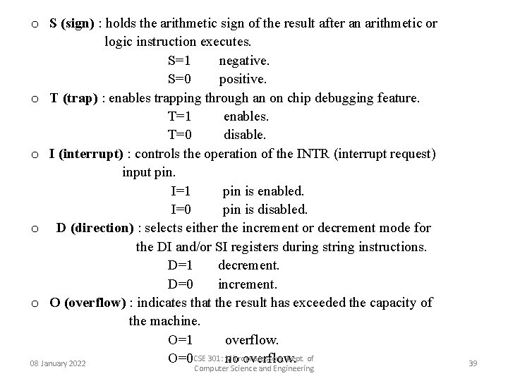
o S (sign) : holds the arithmetic sign of the result after an arithmetic or logic instruction executes. S=1 negative. S=0 positive. o T (trap) : enables trapping through an on chip debugging feature. T=1 enables. T=0 disable. o I (interrupt) : controls the operation of the INTR (interrupt request) input pin. I=1 pin is enabled. I=0 pin is disabled. o D (direction) : selects either the increment or decrement mode for the DI and/or SI registers during string instructions. D=1 decrement. D=0 increment. o O (overflow) : indicates that the result has exceeded the capacity of the machine. O=1 overflow. Microprocessors, Dept. of O=0 CSE 301: no overflow. 08 January 2022 Computer Science and Engineering 39

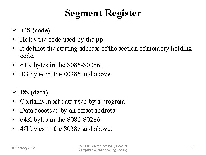
Segment Register ü CS (code) • Holds the code used by the µp. • It defines the starting address of the section of memory holding code. • 64 K bytes in the 8086 -80286. • 4 G bytes in the 80386 and above. ü • • DS (data). Contains most data used by a program Data accessed by an offset address. 64 K bytes in the 8086 -80286. 4 G bytes in the 80386 and above. 08 January 2022 CSE 301: Microprocessors, Dept. of Computer Science and Engineering 40

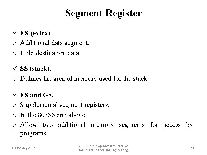
Segment Register ü ES (extra). o Additional data segment. o Hold destination data. ü SS (stack). o Defines the area of memory used for the stack. ü o o o FS and GS. Supplemental segment registers. In the 80386 and above. Allow two additional memory segments for access by programs. 08 January 2022 CSE 301: Microprocessors, Dept. of Computer Science and Engineering 41

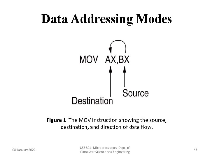
Addressing Modes q Data Addressing Modes • MOV instruction is a common and flexible instruction. – provides a basis for explanation of data-addressing modes • Figure 1 illustrates the MOV instruction and defines the direction of data flow. • Source is to the right and destination the left, next to the opcode MOV. – an opcode, or operation code, tells the microprocessor which operation to perform 08 January 2022 CSE 301: Microprocessors, Dept. of Computer Science and Engineering 42

Data Addressing Modes Figure 1 The MOV instruction showing the source, destination, and direction of data flow. 08 January 2022 CSE 301: Microprocessors, Dept. of Computer Science and Engineering 43

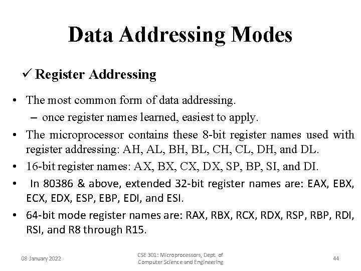
Data Addressing Modes ü Register Addressing • The most common form of data addressing. – once register names learned, easiest to apply. • The microprocessor contains these 8 -bit register names used with register addressing: AH, AL, BH, BL, CH, CL, DH, and DL. • 16 -bit register names: AX, BX, CX, DX, SP, BP, SI, and DI. • In 80386 & above, extended 32 -bit register names are: EAX, EBX, ECX, EDX, ESP, EBP, EDI, and ESI. • 64 -bit mode register names are: RAX, RBX, RCX, RDX, RSP, RBP, RDI, RSI, and R 8 through R 15. 08 January 2022 CSE 301: Microprocessors, Dept. of Computer Science and Engineering 44

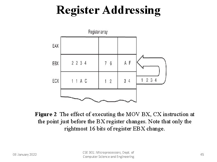
Register Addressing Figure 2 The effect of executing the MOV BX, CX instruction at the point just before the BX register changes. Note that only the rightmost 16 bits of register EBX change. 08 January 2022 CSE 301: Microprocessors, Dept. of Computer Science and Engineering 45

Register Addressing • Figure 2 shows the operation of the MOV BX, CX instruction. • The source register’s contents do not change. – the destination register’s contents do change • The contents of the destination register or destination memory location change for all instructions except the CMP and TEST instructions. • The MOV BX, CX instruction does not affect the leftmost 16 bits of register EBX. 08 January 2022 CSE 301: Microprocessors, Dept. of Computer Science and Engineering 46

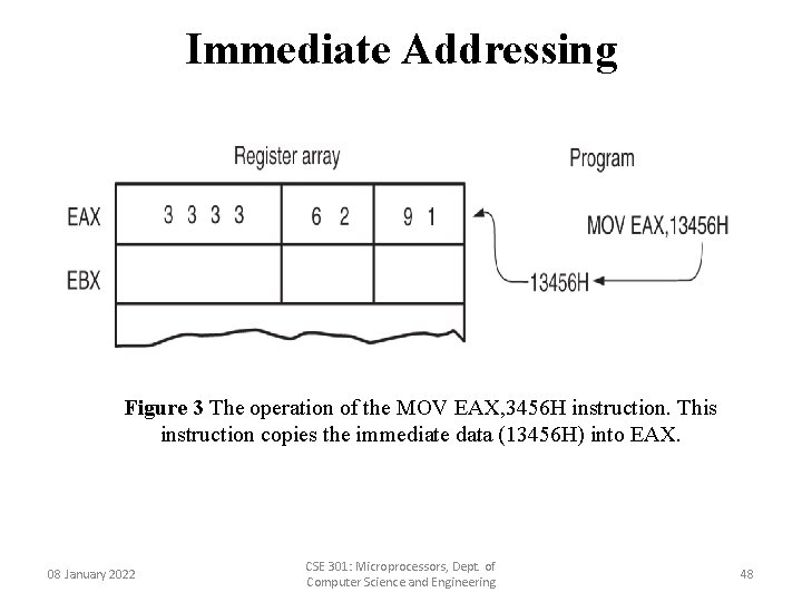
Data Addressing Modes ü Immediate Addressing • Term immediate implies that data immediately follow the hexadecimal opcode in the memory. – immediate data are constant data – data transferred from a register or memory location are variable data • Immediate addressing operates upon a byte or word of data. • Figure 3 shows the operation of a MOV EAX, 13456 H instruction. 08 January 2022 CSE 301: Microprocessors, Dept. of Computer Science and Engineering 47

Immediate Addressing Figure 3 The operation of the MOV EAX, 3456 H instruction. This instruction copies the immediate data (13456 H) into EAX. 08 January 2022 CSE 301: Microprocessors, Dept. of Computer Science and Engineering 48

Immediate Addressing • In symbolic assembly language, the symbol # precedes immediate data in some assemblers. – MOV AX, #3456 H instruction is an example • Most assemblers do not use the # symbol, but represent immediate data as in the MOV AX, 3456 H instruction. 08 January 2022 CSE 301: Microprocessors, Dept. of Computer Science and Engineering 49

Data Addressing Modes ü Direct Data Addressing • Applied to many instructions in a typical program. • Two basic forms of direct data addressing: – direct addressing, which applies to a MOV between a memory location and AL, AX, or EAX – displacement addressing, which applies to almost any instruction in the instruction set • Address is formed by adding the displacement to the default data segment address or an alternate segment address. 08 January 2022 CSE 301: Microprocessors, Dept. of Computer Science and Engineering 50

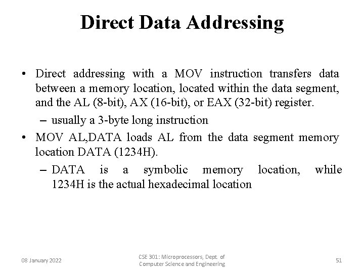
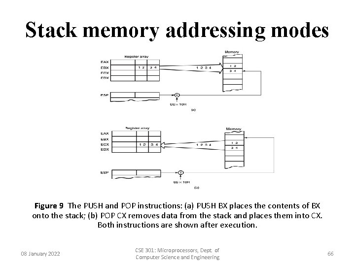
Direct Data Addressing • Direct addressing with a MOV instruction transfers data between a memory location, located within the data segment, and the AL (8 -bit), AX (16 -bit), or EAX (32 -bit) register. – usually a 3 -byte long instruction • MOV AL, DATA loads AL from the data segment memory location DATA (1234 H). – DATA is a symbolic memory location, while 1234 H is the actual hexadecimal location 08 January 2022 CSE 301: Microprocessors, Dept. of Computer Science and Engineering 51
![Direct Data Addressing Figure 4 The operation of the MOV AL 1234 H instruction Direct Data Addressing Figure 4 The operation of the MOV AL, [1234 H] instruction](https://slidetodoc.com/presentation_image_h2/5fc15ab0b86f7a45b8a97989cc45fd53/image-52.jpg)
Direct Data Addressing Figure 4 The operation of the MOV AL, [1234 H] instruction when DS=1000 H. • This instruction transfers a copy contents of memory location 11234 H into AL. – the effective address is formed by adding 1234 H (the offset address) and 10000 H (the data segment address of 1000 H times 10 H) in a system operating in the real mode 08 January 2022 CSE 301: Microprocessors, Dept. of Computer Science and Engineering 52

Data Addressing Modes ü Register Indirect Addressing • Allows data to be addressed at any memory location through an offset address held in any of the following registers: BP, BX, DI, and SI. • In addition, 80386 and above allow register indirect addressing with any extended register except ESP. • In the 64 -bit mode, the segment registers serve no purpose in addressing a location in the flat model. 08 January 2022 CSE 301: Microprocessors, Dept. of Computer Science and Engineering 53
![Register Indirect Addressing Figure 5 The operation of the MOV AX BX instruction when Register Indirect Addressing Figure 5 The operation of the MOV AX, [BX] instruction when](https://slidetodoc.com/presentation_image_h2/5fc15ab0b86f7a45b8a97989cc45fd53/image-54.jpg)
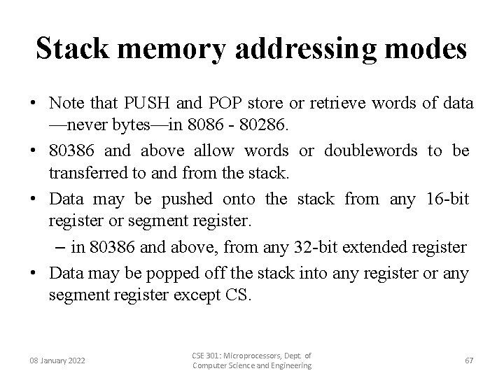
Register Indirect Addressing Figure 5 The operation of the MOV AX, [BX] instruction when BX = 1000 H and DS = 0100 H. Note that this instruction is shown after the contents of memory are transferred to AX. 08 January 2022 CSE 301: Microprocessors, Dept. of Computer Science and Engineering 54

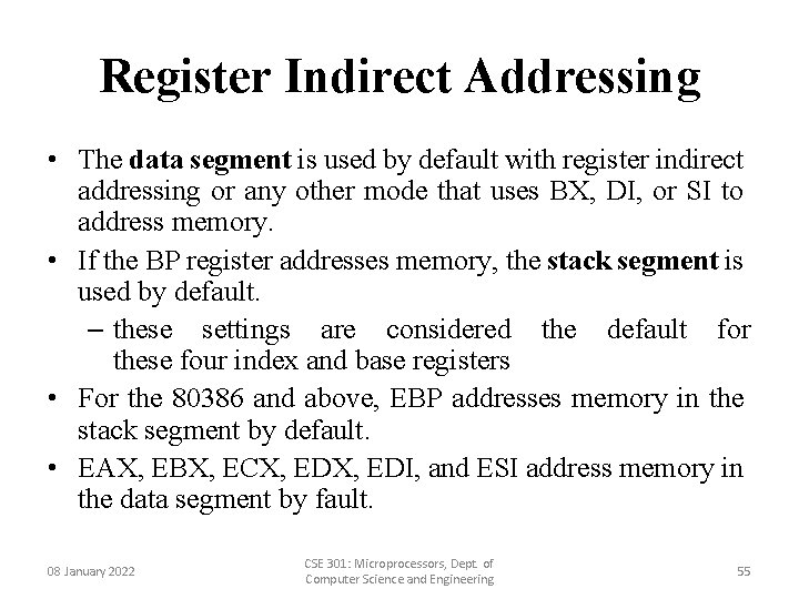
Register Indirect Addressing • The data segment is used by default with register indirect addressing or any other mode that uses BX, DI, or SI to address memory. • If the BP register addresses memory, the stack segment is used by default. – these settings are considered the default for these four index and base registers • For the 80386 and above, EBP addresses memory in the stack segment by default. • EAX, EBX, ECX, EDI, and ESI address memory in the data segment by fault. 08 January 2022 CSE 301: Microprocessors, Dept. of Computer Science and Engineering 55

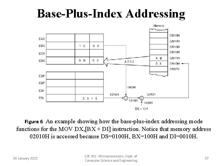
Data Addressing Modes ü Base-Plus-Index Addressing • Similar to indirect addressing because it indirectly addresses memory data. • The base register often holds the beginning location of a memory array. – the index register holds the relative position of an element in the array – whenever BP addresses memory data, both the stack segment register and BP generate the effective address 08 January 2022 CSE 301: Microprocessors, Dept. of Computer Science and Engineering 56

Base-Plus-Index Addressing Figure 6 An example showing how the base-plus-index addressing mode functions for the MOV DX, [BX + DI] instruction. Notice that memory address 02010 H is accessed because DS=0100 H, BX=100 H and DI=0010 H. 08 January 2022 CSE 301: Microprocessors, Dept. of Computer Science and Engineering 57

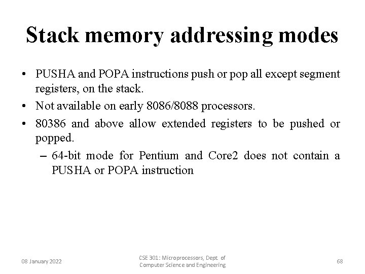
Data Addressing Modes ü Register Relative Addressing • Similar to base-plus-index addressing and displacement addressing. – data in a segment of memory are addressed by adding the displacement to the contents of a base or an index register (BP, BX, DI, or SI) • Figure 7 shows the operation of the MOV AX, [BX+1000 H] instruction. • A real mode segment is 64 K bytes long. 08 January 2022 CSE 301: Microprocessors, Dept. of Computer Science and Engineering 58
![Register Relative Addressing Figure 7 The operation of the MOV AX BX1000 H instructon Register Relative Addressing Figure 7 The operation of the MOV AX, [BX=1000 H] instructon,](https://slidetodoc.com/presentation_image_h2/5fc15ab0b86f7a45b8a97989cc45fd53/image-59.jpg)
Register Relative Addressing Figure 7 The operation of the MOV AX, [BX=1000 H] instructon, when BX=1000 H and DS=0200 H. 08 January 2022 CSE 301: Microprocessors, Dept. of Computer Science and Engineering 59

Data Addressing Modes ü Base Relative-Plus-Index Addressing • Similar to base-plus-index addressing. – adds a displacement – uses a base register and an index register to form the memory address • This type of addressing mode often addresses a twodimensional array of memory data. 08 January 2022 CSE 301: Microprocessors, Dept. of Computer Science and Engineering 60

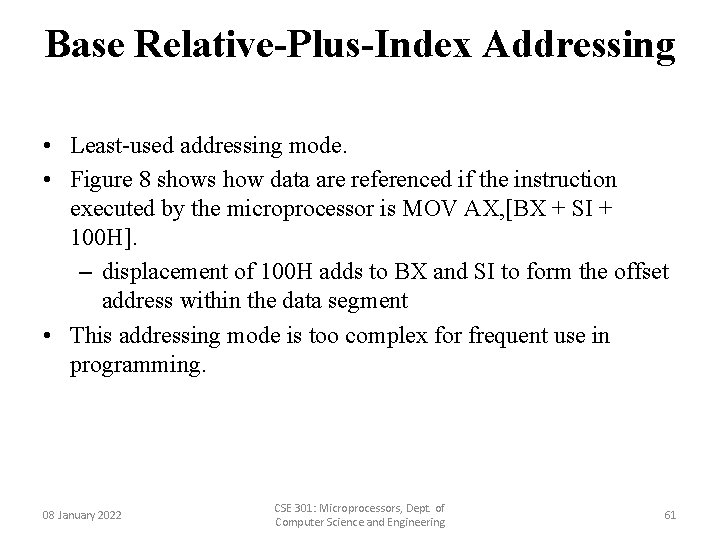
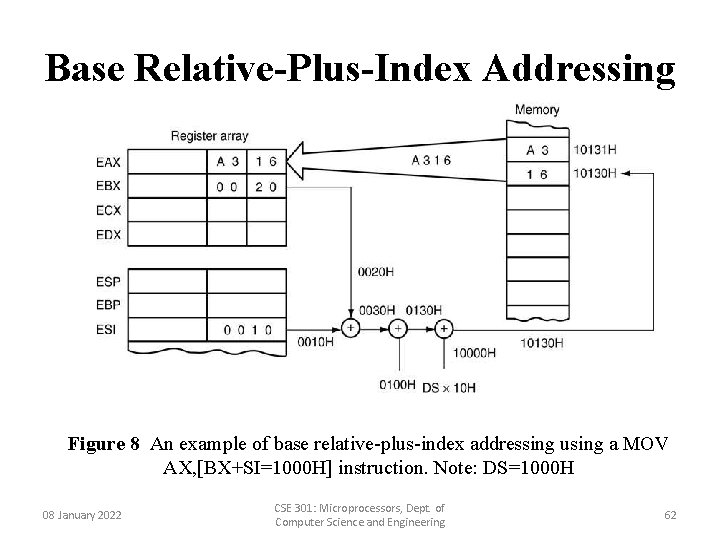
Base Relative-Plus-Index Addressing • Least-used addressing mode. • Figure 8 shows how data are referenced if the instruction executed by the microprocessor is MOV AX, [BX + SI + 100 H]. – displacement of 100 H adds to BX and SI to form the offset address within the data segment • This addressing mode is too complex for frequent use in programming. 08 January 2022 CSE 301: Microprocessors, Dept. of Computer Science and Engineering 61

Base Relative-Plus-Index Addressing Figure 8 An example of base relative-plus-index addressing using a MOV AX, [BX+SI=1000 H] instruction. Note: DS=1000 H 08 January 2022 CSE 301: Microprocessors, Dept. of Computer Science and Engineering 62

Stack memory addressing modes • The stack plays an important role in all microprocessors. – holds data temporarily and stores return addresses used by procedures • Stack memory is LIFO (last-in, first-out) memory – describes the way data are stored and removed from the stack 08 January 2022 CSE 301: Microprocessors, Dept. of Computer Science and Engineering 63

Stack memory addressing modes • Data are placed on the stack with a PUSH instruction; removed with a POP instruction. • Stack memory is maintained by two registers: – the stack pointer (SP or ESP) – the stack segment register (SS) • Whenever a word of data is pushed onto the stack, the high-order 8 bits are placed in the location addressed by SP – 1. – low-order 8 bits are placed in the location addressed by SP – 2 08 January 2022 CSE 301: Microprocessors, Dept. of Computer Science and Engineering 64

Stack memory addressing modes • The SP is decremented by 2 so the next word is stored in the next available stack location. – the SP/ESP register always points to an area of memory located within the stack segment. • In protected mode operation, the SS register holds a selector that accesses a descriptor for the base address of the stack segment. • When data are popped from the stack, the low-order 8 bits are removed from the location addressed by SP. – high-order 8 bits are removed; the SP register is incremented by 2 08 January 2022 CSE 301: Microprocessors, Dept. of Computer Science and Engineering 65

Stack memory addressing modes Figure 9 The PUSH and POP instructions: (a) PUSH BX places the contents of BX onto the stack; (b) POP CX removes data from the stack and places them into CX. Both instructions are shown after execution. 08 January 2022 CSE 301: Microprocessors, Dept. of Computer Science and Engineering 66

Stack memory addressing modes • Note that PUSH and POP store or retrieve words of data —never bytes—in 8086 - 80286. • 80386 and above allow words or doublewords to be transferred to and from the stack. • Data may be pushed onto the stack from any 16 -bit register or segment register. – in 80386 and above, from any 32 -bit extended register • Data may be popped off the stack into any register or any segment register except CS. 08 January 2022 CSE 301: Microprocessors, Dept. of Computer Science and Engineering 67

Stack memory addressing modes • PUSHA and POPA instructions push or pop all except segment registers, on the stack. • Not available on early 8086/8088 processors. • 80386 and above allow extended registers to be pushed or popped. – 64 -bit mode for Pentium and Core 2 does not contain a PUSHA or POPA instruction 08 January 2022 CSE 301: Microprocessors, Dept. of Computer Science and Engineering 68

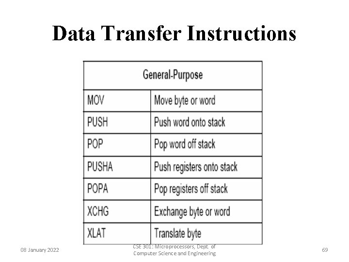
Data Transfer Instructions 08 January 2022 CSE 301: Microprocessors, Dept. of Computer Science and Engineering 69

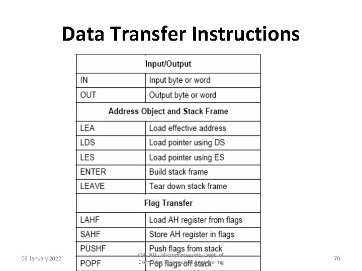
Data Transfer Instructions 08 January 2022 CSE 301: Microprocessors, Dept. of Computer Science and Engineering 70

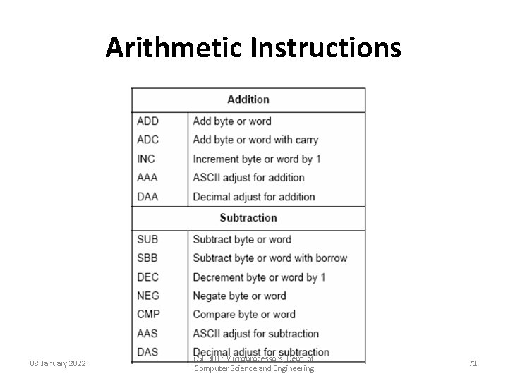
Arithmetic Instructions 08 January 2022 CSE 301: Microprocessors, Dept. of Computer Science and Engineering 71

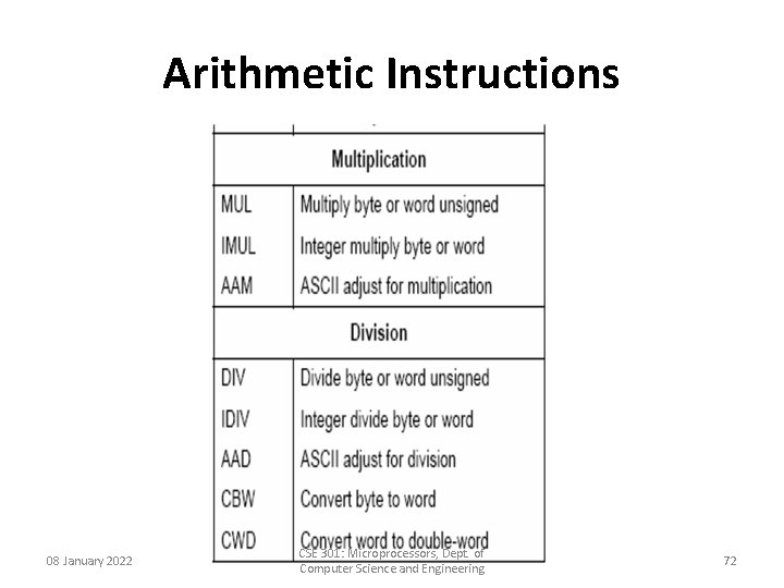
Arithmetic Instructions 08 January 2022 CSE 301: Microprocessors, Dept. of Computer Science and Engineering 72

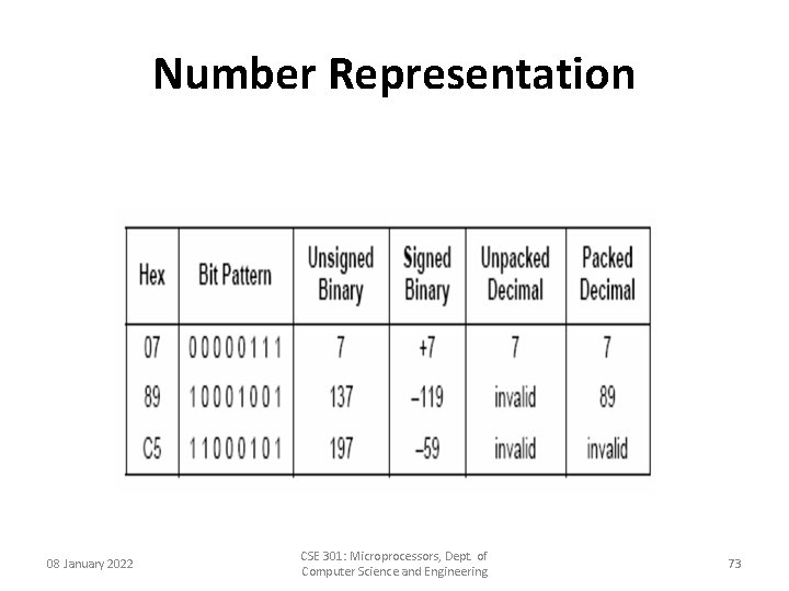
Number Representation 08 January 2022 CSE 301: Microprocessors, Dept. of Computer Science and Engineering 73

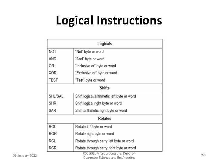
Logical Instructions 08 January 2022 CSE 301: Microprocessors, Dept. of Computer Science and Engineering 74

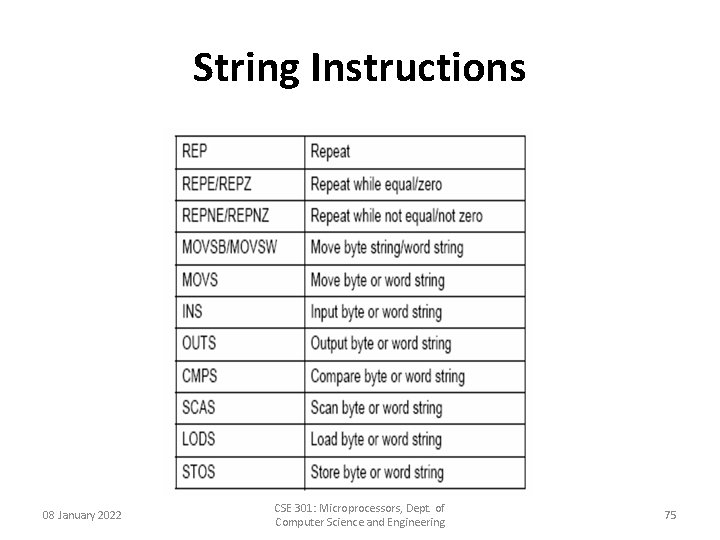
String Instructions 08 January 2022 CSE 301: Microprocessors, Dept. of Computer Science and Engineering 75

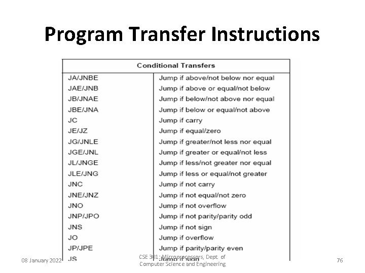
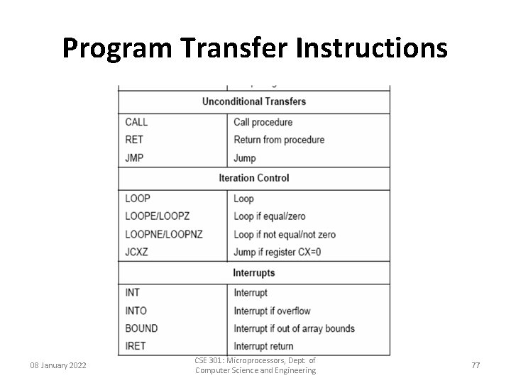
Program Transfer Instructions 08 January 2022 CSE 301: Microprocessors, Dept. of Computer Science and Engineering 76

Program Transfer Instructions 08 January 2022 CSE 301: Microprocessors, Dept. of Computer Science and Engineering 77

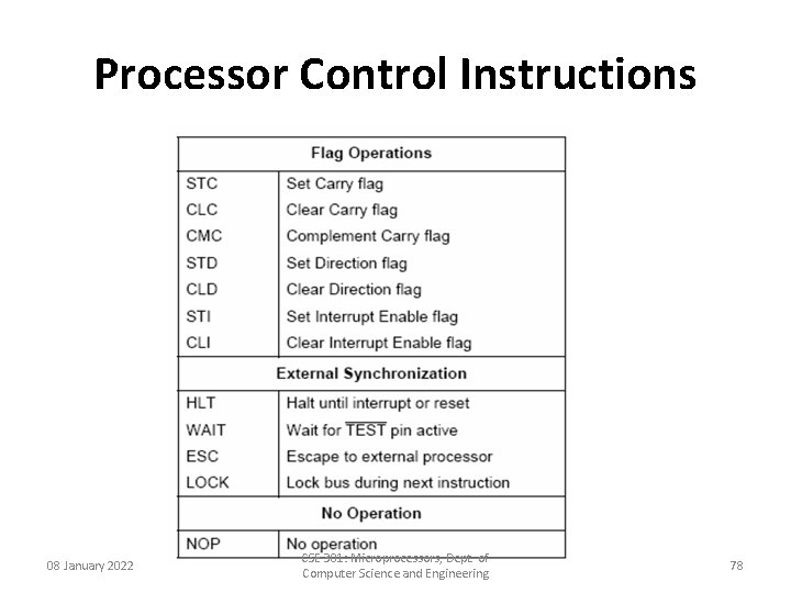
Processor Control Instructions 08 January 2022 CSE 301: Microprocessors, Dept. of Computer Science and Engineering 78

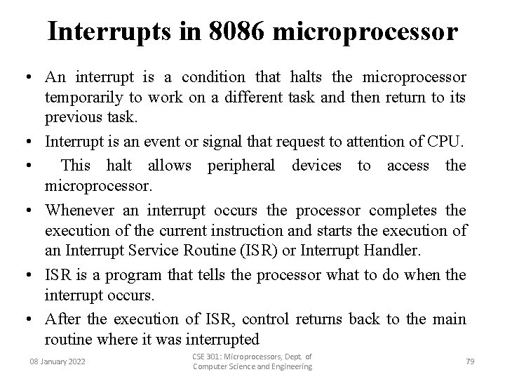
Interrupts in 8086 microprocessor • An interrupt is a condition that halts the microprocessor temporarily to work on a different task and then return to its previous task. • Interrupt is an event or signal that request to attention of CPU. • This halt allows peripheral devices to access the microprocessor. • Whenever an interrupt occurs the processor completes the execution of the current instruction and starts the execution of an Interrupt Service Routine (ISR) or Interrupt Handler. • ISR is a program that tells the processor what to do when the interrupt occurs. • After the execution of ISR, control returns back to the main routine where it was interrupted 08 January 2022 CSE 301: Microprocessors, Dept. of Computer Science and Engineering 79

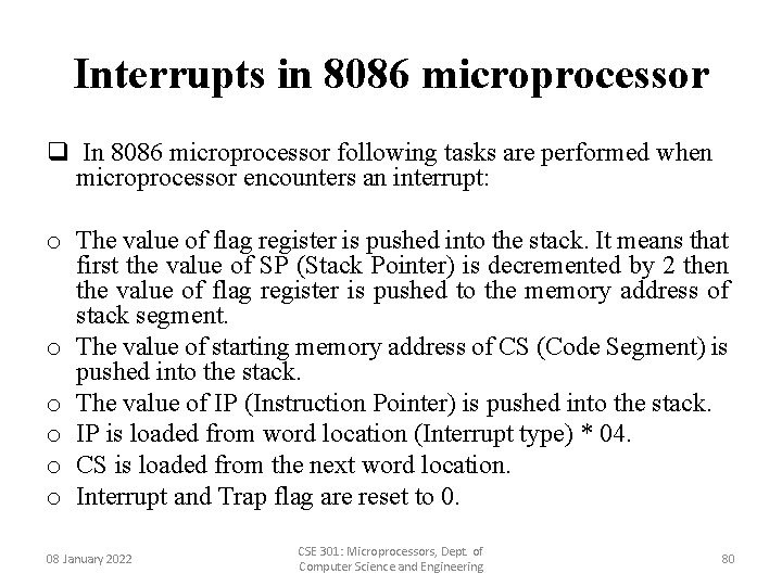
Interrupts in 8086 microprocessor q In 8086 microprocessor following tasks are performed when microprocessor encounters an interrupt: o The value of flag register is pushed into the stack. It means that first the value of SP (Stack Pointer) is decremented by 2 then the value of flag register is pushed to the memory address of stack segment. o The value of starting memory address of CS (Code Segment) is pushed into the stack. o The value of IP (Instruction Pointer) is pushed into the stack. o IP is loaded from word location (Interrupt type) * 04. o CS is loaded from the next word location. o Interrupt and Trap flag are reset to 0. 08 January 2022 CSE 301: Microprocessors, Dept. of Computer Science and Engineering 80

Interrupts in 8086 microprocessor ü Types of interrupts o Hardware Interrupts • Hardware interrupts are those interrupts which are caused by any peripheral device by sending a signal through a specified pin to the microprocessor. • There are two hardware interrupts in 8086 microprocessor. They are: § (A) NMI (Non Maskable Interrupt) – • It is a single pin non maskable hardware interrupt which cannot be disabled. • It is the highest priority interrupt in 8086 microprocessor. • After its execution, this interrupt generates a TYPE 2 interrupt. • IP is loaded from word location 00008 H and CS is loaded from the word location 0000 A H. 08 January 2022 CSE 301: Microprocessors, Dept. of Computer Science and Engineering 81

Interrupts in 8086 microprocessor § (B) INTR (Interrupt Request) – • It provides a single interrupt request and is activated by I/O port. • This interrupt can be masked or delayed. • It is a level triggered interrupt. It can receive any interrupt type, so the value of IP and CS will change on the interrupt type received. 08 January 2022 CSE 301: Microprocessors, Dept. of Computer Science and Engineering 82

Interrupts in 8086 microprocessor ü Software Interrupts – These are instructions that are inserted within the program to generate interrupts. There are 256 software interrupts in 8086 microprocessor. The instructions are of the format INT type where type ranges from 00 to FF. The starting address ranges from 00000 H to 003 FF H. These are 2 byte instructions. IP is loaded from type * 04 H and CS is loaded from the next address give by (type * 04) + 02 H. Some important software interrupts are: • TYPE 0 corresponds to division by zero(0). • TYPE 1 is used for single step execution for debugging of program. • TYPE 2 represents NMI and is used in power failure conditions. • TYPE 3 represents a break-point interrupt. • TYPE 4 is the overflow interrupt 08 January 2022 CSE 301: Microprocessors, Dept. of Computer Science and Engineering 83