CSE 301 Microprocessors Dr Md Sujan Ali Associate
- Slides: 71

CSE 301 Microprocessors Dr. Md. Sujan Ali Associate Professor Dept. of Computer Science and Engineering Jatiya Kabi Kazi Nazrul Islam University Trishal, Mymensingh, Bangladesh

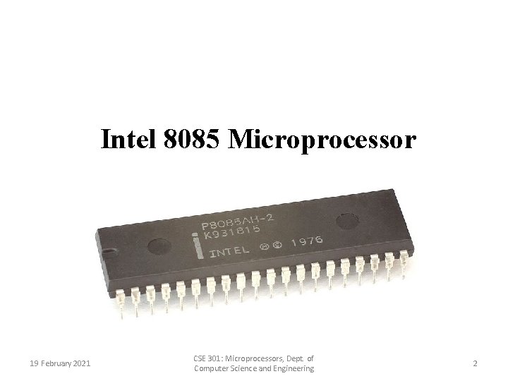
Intel 8085 Microprocessor 19 February 2021 CSE 301: Microprocessors, Dept. of Computer Science and Engineering 2

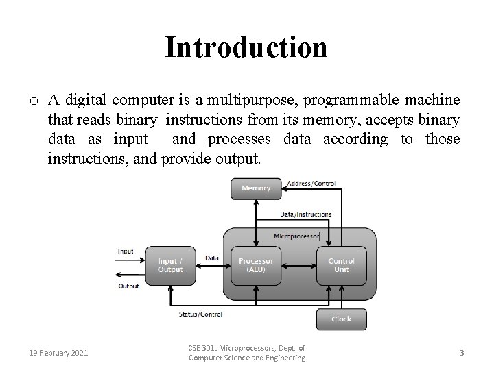
Introduction o A digital computer is a multipurpose, programmable machine that reads binary instructions from its memory, accepts binary data as input and processes data according to those instructions, and provide output. 19 February 2021 CSE 301: Microprocessors, Dept. of Computer Science and Engineering 3

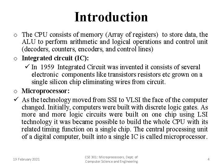
Introduction o The CPU consists of memory (Array of registers) to store data, the ALU to perform arithmetic and logical operations and control unit (decoders, counters, encoders, and control lines) o Integrated circuit (IC): ü In 1959 Integrated Circuit was invented it consists of several electronic components like transistors resistors etc grown on a single silicon chip eliminating wires from circuit. o Microprocessor: ü As the technology moved from SSI to VLSI the face of the computer changed. Initially, computers were built with discrete logic gates. As more and more logic circuits were built on one chip using LSI technology it was became possible to build the whole CPU with its related timing function on a single chip. The central processing unit of a digital computer, built into a single IC is called microprocessor. 19 February 2021 CSE 301: Microprocessors, Dept. of Computer Science and Engineering 4

Introduction to 8085 Introduced in 1977. It is 8 -bit MP. Capable of addressing 64 k of memory It is a 40 pin dual-in-line chip. It uses a single +5 V supply for its operations. This processor is available in three versions such as 8085 AH, 8085 AH 1, and 8085 AH 2 which are designed with HMOS technology. o The highly developed versions use 20% of the power supply. o The CLK frequencies of the versions of this processor are 8085 A- 3 MHz, 8085 AH-3 MHz, 8085 AH 2 -5 MHz, and 8085 AH 1 -6 MHz. o o o 19 February 2021 CSE 301: Microprocessors, Dept. of Computer Science and Engineering 5

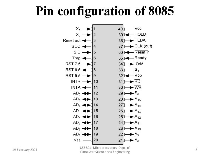
Pin configuration of 8085 19 February 2021 CSE 301: Microprocessors, Dept. of Computer Science and Engineering 6

Pin description of 8085 (cont’d) o Address Bus (A 8 -A 15) • The address bus pins are ranges from A 8 to A 15 and these are mainly applicable to the most considerable memory address bit. o Address Bus (or) Data Bus (AD 0 -AD 7) • The address bus pins or data bus pins are ranges from AD 0 to AD 7, and these pins are applicable for LSB (least significant bits) of the address bus in the primary apparatus CLK cycle as well as employed as a data bus for second clock cycle & third clock cycle. 19 February 2021 CSE 301: Microprocessors, Dept. of Computer Science and Engineering 7

Pin description of 8085 (cont’d) o Address Latch Enable (ALE) • Basically, ALE assists in de-multiplexing the data bus as well as low order address. • This will go high throughout the primary clock cycle as well as allows the address bits with low order. • The address bus with low order is added for memory otherwise any exterior latch. o Status Signal (IO/M) • The status signal IO/M resolves whether the address is intended for memory or input/output. • When the address is high then the address of the address bus is used for the devices of input/output devices. • When the address is low then the address of the address bus is used for the memory. 19 February 2021 CSE 301: Microprocessors, Dept. of Computer Science and Engineering 8

Pin description of 8085 (cont’d) o Status Signals (S 0 -S 1) • The status signals S 0, S 1 gives different functions as well as status based on their status. • When the S 0, S 1 are 01 then the operation will be HALT. • the S 0, S 1 is 10 then the operation will be WRITE • When the S 0, S 1 is 10 then the operation will be READ • When the S 0, S 1 are 11 then the operation will be FETCH 19 February 2021 CSE 301: Microprocessors, Dept. of Computer Science and Engineering 9

Pin description of 8085 (cont’d) o Active Low Signal (RD) • The RD is an energetic low signal and an operation is executed whenever the indication goes small, and it is used for controlling the microprocessor READ operation. • When RD pin goes small then the 8085 microprocessor understands the information from I/O device or memory. o Active Low Signal (WR) • This is an energetic low signal, and it controls the microprocessor’s write operations. • Whenever WR pin goes small, then the information will be written to the I/O device or memory. 19 February 2021 CSE 301: Microprocessors, Dept. of Computer Science and Engineering 10

Pin description of 8085 (cont’d) o READY • The READY pin is employed with the 8085 microprocessor for ensuring whether a device is set for accepting or transferring data. • A device may be an A/D converter or LCD display, etc. These devices are associated with the 8085 microprocessor with the READY-pin. • When this pin is high, the device is prepared for transferring the information, if it is not then the microprocessor stays until this pin goes high. 19 February 2021 CSE 301: Microprocessors, Dept. of Computer Science and Engineering 11

Pin description of 8085 (cont’d) o HOLD • The HOLD pin specifies when any device is demanding the employ of address as well as a data bus. The two devices are LCD as well as A/D converter. • Assume that if A/D converter is employing the address bus as well as a data bus. • When LCD desires the utilize of both the buses by providing HOLD signal, subsequently the microprocessor transmits the control signal toward the LCD after that the existing cycle will be ended. • When the LCD procedure is over, then the control signal is transmitted reverse to A/D converter. 19 February 2021 CSE 301: Microprocessors, Dept. of Computer Science and Engineering 12

Pin description of 8085 (cont’d) o HLDA • This is the response signal of HOLD, and it specifies whether this signal is obtained or not obtained. • After the implementation of HOLD demand, this signal will go low. o INTR • This is an interrupt signal, and the priority of this among the interrupts is low. • This signal can be allowed or not allowed by the software. • When INTR pin goes high then the 8085 microprocessor completes the instruction of current which is being executed and then recognizes the INTR signal and progresses it. 19 February 2021 CSE 301: Microprocessors, Dept. of Computer Science and Engineering 13

Pin description of 8085 (cont’d) o INTA • When the 8085 microprocessor gets an interrupt signal, then it should be recognized. • This will be done by INTA. • As a result, when the interrupt will be obtained then INTA will go high. o RST 5. 5, RST 6. 5, RST 7. 5 • These pins are the restart maskable interrupts or Vectored Interrupts, used to insert an inner restart function repeatedly. • All these interrupts are maskable, they can be allowed or not allowed by using programs. 19 February 2021 CSE 301: Microprocessors, Dept. of Computer Science and Engineering 14

Pin description of 8085 (cont’d) o TRAP • Along with the 8085 microprocessor interrupts, TRAP is a non -maskable interrupt, and it doesn’t allow or stopped by a program. • TRAP has the maximum precedence between the interrupts. • The priority order from maximum to low includes TRAP, RST 5. 5, RST 6. 5, RST 7. 5, and INTR. o RESET IN • RESET IN pin is used to reset the program counter toward zero and rearranges interrupt enable as well as HLDA flipflops (FFs). • The central processing unit is detained in RST condition till this pin is high. • But the registers as well as flags won’t get damaged apart from instruction register. 19 February 2021 CSE 301: Microprocessors, Dept. of Computer Science and Engineering 15

Pin description of 8085 (cont’d) o RST (RESET) OUT • RESET OUT pin specifies that the central processing unit has been rearranged with RST IN. o X 1 X 2 • X 1, X 2 terminals that are associated with the exterior oscillator for generating the required as well as appropriate operation of a clock. o CLK • Sometimes it is compulsory to generate CLK o/PS from 8085 microprocessors so they can be used in favor of other peripherals or else other digital integrated circuits. • This is offered with CLK pin. Its frequency is continually similar because the frequency at which the microprocessor works. 19 February 2021 CSE 301: Microprocessors, Dept. of Computer Science and Engineering 16

Pin description of 8085 o SID • This is a serial i/p data, and the information on this pin is uploaded into the 7 th-bit of the accumulator while RIM (Read Interrupt Mask) instruction is performed. • RIM verifies the interrupt whether it is covered or not covered. o SOD • This is the serial o/p data, and the data on this pin sends its output toward the 7 th-bit of the accumulator whenever an instruction of SIM is performed. o VSS and VCC • VSS is a ground pin whereas Vcc is +5 v pin. 19 February 2021 CSE 301: Microprocessors, Dept. of Computer Science and Engineering 17

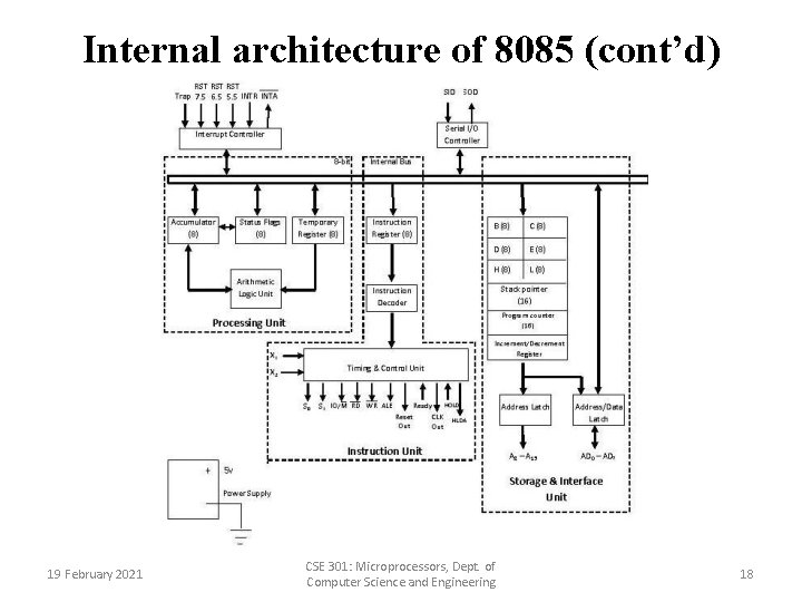
Internal architecture of 8085 (cont’d) 19 February 2021 CSE 301: Microprocessors, Dept. of Computer Science and Engineering 18

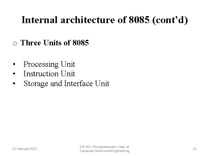
Internal architecture of 8085 (cont’d) o Three Units of 8085 • Processing Unit • Instruction Unit • Storage and Interface Unit 19 February 2021 CSE 301: Microprocessors, Dept. of Computer Science and Engineering 19

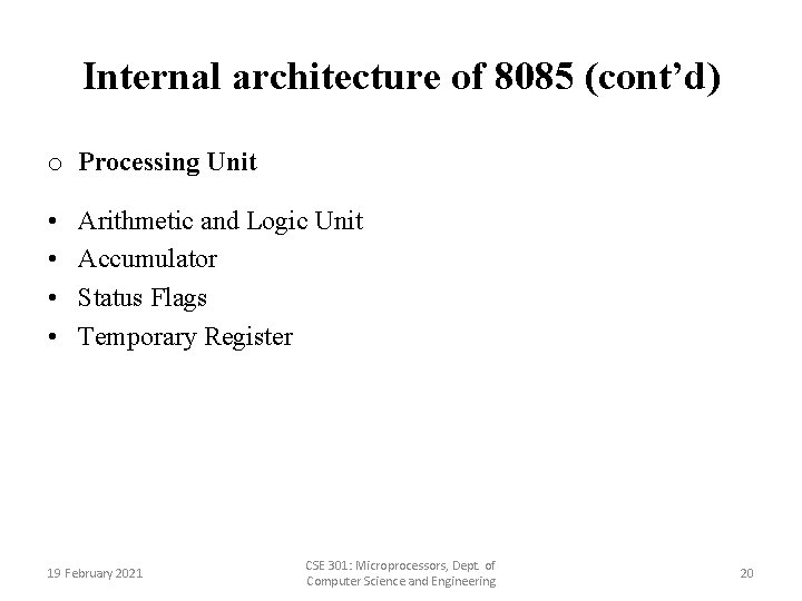
Internal architecture of 8085 (cont’d) o Processing Unit • • Arithmetic and Logic Unit Accumulator Status Flags Temporary Register 19 February 2021 CSE 301: Microprocessors, Dept. of Computer Science and Engineering 20

Internal architecture of 8085 (cont’d) o Instruction Unit • Instruction Register • Instruction Decoder • Timing and Control Unit 19 February 2021 CSE 301: Microprocessors, Dept. of Computer Science and Engineering 21

Internal architecture of 8085 (cont’d) o Storage and Interface Unit • • • General Purpose Registers Stack Pointer Program Counter Increment/Decrement Register Address Latch Address/Data Latch 19 February 2021 CSE 301: Microprocessors, Dept. of Computer Science and Engineering 22

Internal architecture of 8085 (cont’d) o Three Other Units • Interrupt Controller • Serial I/O Controller • Power Supply 19 February 2021 CSE 301: Microprocessors, Dept. of Computer Science and Engineering 23

Internal architecture of 8085 (cont’d) o Accumulator • • • It the main register of microprocessor. It is also called register ‘A’. It is an 8 -bit register. It is used in the arithmetic and logic operations. It always contains one of the operands on which arithmetic/logic has to be performed. • After the arithmetic/logic operation, the contents of accumulator are replaced by the result. 19 February 2021 CSE 301: Microprocessors, Dept. of Computer Science and Engineering 24

Internal architecture of 8085 (cont’d) o Arithmetic and Logic Unit • It performs various arithmetic and logic operations. • The data is available in accumulator and temporary/general purpose registers. • Arithmetic Operations: – Addition, Subtraction, Increment, Decrement etc. • Logic Operations: – AND, OR, X-OR, Complement etc. 19 February 2021 CSE 301: Microprocessors, Dept. of Computer Science and Engineering 25

Internal architecture of 8085 (cont’d) o Temporary Register • It is an 8 -bit register. • It is used to store temporary 8 -bit operand from general purpose register. • It is also used to store intermediate results. 19 February 2021 CSE 301: Microprocessors, Dept. of Computer Science and Engineering 26

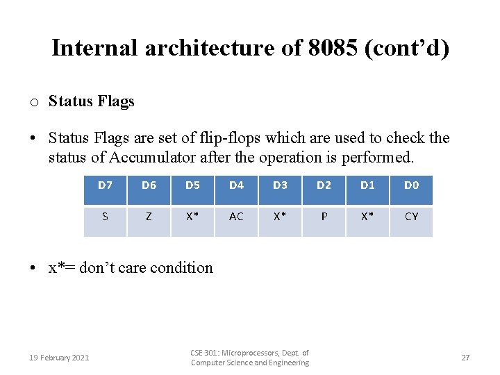
Internal architecture of 8085 (cont’d) o Status Flags • Status Flags are set of flip-flops which are used to check the status of Accumulator after the operation is performed. D 7 D 6 D 5 D 4 D 3 D 2 D 1 D 0 S Z X* AC X* P X* CY • x*= don’t care condition 19 February 2021 CSE 301: Microprocessors, Dept. of Computer Science and Engineering 27

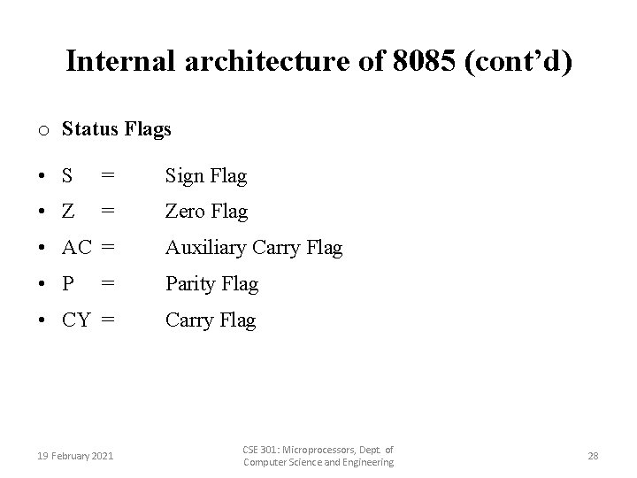
Internal architecture of 8085 (cont’d) o Status Flags • S = Sign Flag • Z = Zero Flag • AC = Auxiliary Carry Flag • P = Parity Flag • CY = Carry Flag 19 February 2021 CSE 301: Microprocessors, Dept. of Computer Science and Engineering 28

Internal architecture of 8085 (cont’d) o Sign Flag (S): – It tells the sign of result stored in Accumulator after the operation is performed. – If result is –ve, sign flag is set (1). – If result is +ve, sign flag is reset (0). 19 February 2021 CSE 301: Microprocessors, Dept. of Computer Science and Engineering 29

Internal architecture of 8085 (cont’d) o Zero Flag (Z): – It tells whether the result stored in Accumulator is zero or not after the operation is performed. – If result is zero, zero flag is set (1). – If result is not zero, zero flag is reset (0). 19 February 2021 CSE 301: Microprocessors, Dept. of Computer Science and Engineering 30

Internal architecture of 8085 (cont’d) o Auxiliary Carry Flag (AC): – It is used in BCD operations. – When there is carry in BCD addition, we add 0110 (6) to the result. – If there is carry in BCD addition, auxiliary carry is set (1). – If there is no carry, auxiliary carry is reset (0). 19 February 2021 CSE 301: Microprocessors, Dept. of Computer Science and Engineering 31

Internal architecture of 8085 (cont’d) o Parity Flag (P): – It tells the parity of data stored in Accumulator. – If parity is even, parity flag is set (1). – If parity is odd, parity flag is reset (0). 19 February 2021 CSE 301: Microprocessors, Dept. of Computer Science and Engineering 32

Internal architecture of 8085 (cont’d) o Program Status Word (PSW) • In a flag register five bits (D 0, D 2, D 4, D 6, D 7) indicate status and three bits (D 5, D 3, D 1) is undefined • Combination of these 8 bits known as Program Status Word (PSW) 19 February 2021 CSE 301: Microprocessors, Dept. of Computer Science and Engineering 33

Internal architecture of 8085 (cont’d) o Instruction Register • It is used to hold the current instruction which the microprocessor is about to execute. • It is an 8 -bit register. 19 February 2021 CSE 301: Microprocessors, Dept. of Computer Science and Engineering 34

Internal architecture of 8085 (cont’d) o Instruction Decoder • It interprets the instruction stored in instruction register. • It generates various machine cycles depending upon the instruction. • The machine cycles are then given to the Timing and Control Unit. 19 February 2021 CSE 301: Microprocessors, Dept. of Computer Science and Engineering 35

Internal architecture of 8085 (cont’d) o Timing and Control Unit • It controls all the operations of microprocessor and peripheral devices. • Depending upon the machine cycles received from Instruction Decoder, it generates 12 control signals: – S 0 and S 1 (Status Signals). – ALE (Address Latch Enable). 19 February 2021 CSE 301: Microprocessors, Dept. of Computer Science and Engineering 36

Internal architecture of 8085 (cont’d) o Timing and Control Unit – RD (Read, active low). – WR (Write, active low). – IO/M (Input-Output/Memory). – READY – RESET IN – RESET OUT – CLK OUT – HOLD and HLDA 19 February 2021 CSE 301: Microprocessors, Dept. of Computer Science and Engineering 37

Internal architecture of 8085 (cont’d) o General Purpose Registers • There are 6 general purpose registers, namely B, C, D, E, H, L. • Each of them is 8 -bit register. • They are used to hold data and results. • To hold 16 -bit data, combination of two 8 -bit registers can be used. • This combination is known as Register Pair. • The valid register pairs are: – B – C, D – E, H – L. 19 February 2021 CSE 301: Microprocessors, Dept. of Computer Science and Engineering 38

Internal architecture of 8085 (cont’d) o Program Counter • It is used to hold the address of next instruction to be executed. • It is a 16 -bit register. • The microprocessor increments the value of Program Counter after the execution of the current instruction, so that, it always points to the next instruction. 19 February 2021 CSE 301: Microprocessors, Dept. of Computer Science and Engineering 39

Internal architecture of 8085 (cont’d) o Stack Pointer • It holds the address of top most item in the stack. • It is also 16 -bit register. • Any portion of memory can be used as stack. 19 February 2021 CSE 301: Microprocessors, Dept. of Computer Science and Engineering 40

Internal architecture of 8085 (cont’d) o Increment/Decrement Register • This register is used to increment or decrement the value of Stack Pointer. • During PUSH operation, the value of Stack Pointer is incremented. • During POP operation, the value of Stack Pointer is decremented. 19 February 2021 CSE 301: Microprocessors, Dept. of Computer Science and Engineering 41

Internal architecture of 8085 (cont’d) o Address Latch • It is group of 8 buffers. • The upper-byte of 16 -bit address is stored in this latch. • And then it is made available to the peripheral devices. 19 February 2021 CSE 301: Microprocessors, Dept. of Computer Science and Engineering 42

Internal architecture of 8085 (cont’d) o Address/Data Latch • • The lower-byte of address and 8 -bit of data are multiplexed. It holds either lower-byte of address or 8 -bits of data. This is decided by ALE (Address Latch Enable) signal. If ALE = 1 then – Address/Data Latch contains lower-byte of address. • If ALE = 0 then – It contains 8 -bit data. 19 February 2021 CSE 301: Microprocessors, Dept. of Computer Science and Engineering 43

Internal architecture of 8085 (cont’d) o Serial I/O Controller • It is used to convert serial data into parallel and parallel data into serial. • Microprocessor works with 8 -bit parallel data. • Serial I/O devices works with serial transfer of data. • Therefore, this unit is the interface between microprocessor and serial I/O devices. 19 February 2021 CSE 301: Microprocessors, Dept. of Computer Science and Engineering 44

Internal architecture of 8085 (cont’d) o Interrupt Controller • It is used to handle the interrupts. • There are 5 interrupt signals in 8085: – TRAP – RST 7. 5 – RST 6. 5 – RST 5. 5 – INTR 19 February 2021 CSE 301: Microprocessors, Dept. of Computer Science and Engineering 45

Internal architecture of 8085 (cont’d) o Interrupt Controller • Interrupt controller receives these interrupts according to their priority and applies them to the microprocessor. • There is one outgoing signal INTA which is called Interrupt Acknowledge. 19 February 2021 CSE 301: Microprocessors, Dept. of Computer Science and Engineering 46

Internal architecture of 8085 o Power Supply • This unit provides +5 V power supply to the microprocessor. • The microprocessor needs +5 V power supply for its operation. 19 February 2021 CSE 301: Microprocessors, Dept. of Computer Science and Engineering 47

Operation of 8085 microprocessor o It performance four different operations • Memory read • Memory write • Input/output read • Input/output write 19 February 2021 CSE 301: Microprocessors, Dept. of Computer Science and Engineering 48

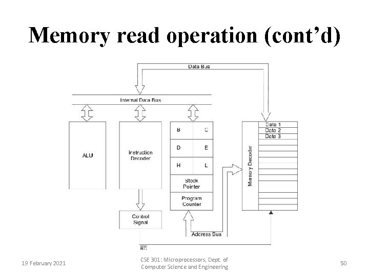
Memory read operation (cont’d) o Microprocessor place 16 bit address in to the address bus. o Decoding the address bus for identifying the memory address of data. o Microprocessor sends controls signal enable the memory IC. o Data of memory location is placed in data bus and microprocessor o The 16 bit memory address is stored into program counter o Program counter sends the 16 bit address on the address bus o Memory address decoder is decoded and identified the specified memory location 19 February 2021 CSE 301: Microprocessors, Dept. of Computer Science and Engineering 49

Memory read operation (cont’d) 19 February 2021 CSE 301: Microprocessors, Dept. of Computer Science and Engineering 50

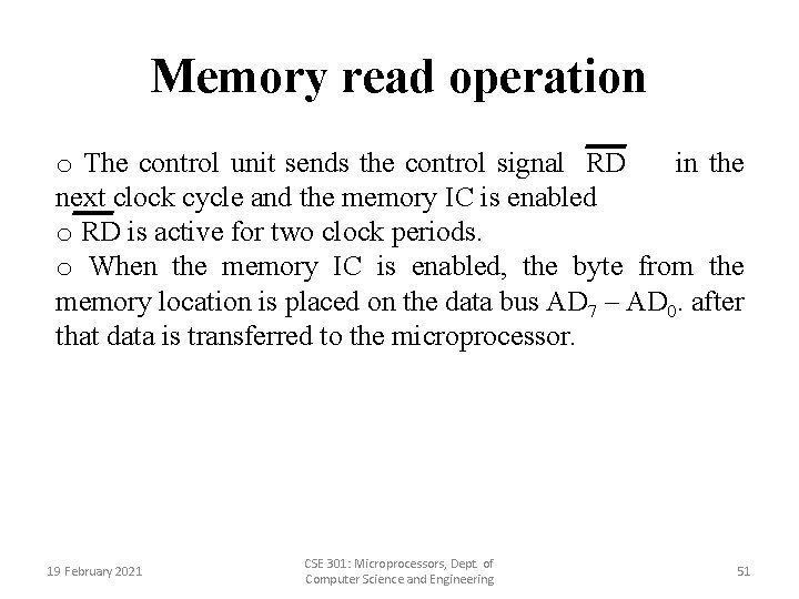
Memory read operation o The control unit sends the control signal RD in the next clock cycle and the memory IC is enabled o RD is active for two clock periods. o When the memory IC is enabled, the byte from the memory location is placed on the data bus AD 7 – AD 0. after that data is transferred to the microprocessor. 19 February 2021 CSE 301: Microprocessors, Dept. of Computer Science and Engineering 51

Addressing modes of 8085 microprocessor (cont’d) Each instruction performs an operation on the specified data called operand. An operand must be specified for an instruction to be executed. o The operand may be in the general purpose register, accumulator or in a memory location. o The way in which the operand is specified for an instruction is called addressing mode. o Various addressing modes used in MP 8085 are: 1. Direct Addressing 2. Register Addressing 3. Register Indirect Addressing 4. Immediate Addressing. 5. Implicit Addressing o 19 February 2021 CSE 301: Microprocessors, Dept. of Computer Science and Engineering 52

Addressing modes of 8085 microprocessor (cont’d) ü Direct addressing o In this mode of addressing the address of the operand (data) is given in the instruction itself. For example: 1. 19 February 2021 CSE 301: Microprocessors, Dept. of Computer Science and Engineering 53

Addressing modes of 8085 microprocessor (cont’d) ü Register Addressing o In register addressing mode the operands are in the general purpose registers. For example: 1. 19 February 2021 CSE 301: Microprocessors, Dept. of Computer Science and Engineering 54

Addressing modes of 8085 microprocessor (cont’d) ü Register indirect addressing o In this mode of addressing the address of the operand (data) is specified by a register pair. For example: 1. LXI H, 2500 H: 19 February 2021 CSE 301: Microprocessors, Dept. of Computer Science and Engineering 55

Addressing modes of 8085 microprocessor (cont’d) ü Immediate Addressing o In immediate addressing mode the operands are specified within the instruction itself. For example: 1. MVI A, 05 : Move 05 in the Accumulator. 2. ADI 06 : Add 06 to the contents of the accumulator. 19 February 2021 CSE 301: Microprocessors, Dept. of Computer Science and Engineering 56

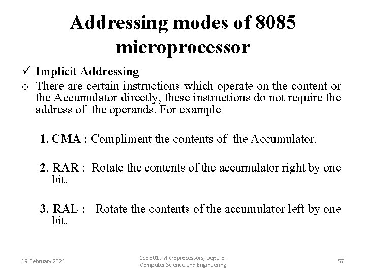
Addressing modes of 8085 microprocessor ü Implicit Addressing o There are certain instructions which operate on the content or the Accumulator directly, these instructions do not require the address of the operands. For example 1. CMA : Compliment the contents of the Accumulator. 2. RAR : Rotate the contents of the accumulator right by one bit. 3. RAL : Rotate the contents of the accumulator left by one bit. 19 February 2021 CSE 301: Microprocessors, Dept. of Computer Science and Engineering 57

Instruction Set of 8085 (cont’d) o An instruction is a binary pattern designed inside a microprocessor to perform a specific function. o The entire group of instructions that a microprocessor supports is called Instruction Set. o 8085 has 246 instructions. o Each instruction is represented by an 8 -bit binary value. o These 8 -bits of binary value is called Op-Codeor Instruction Byte. 19 February 2021 CSE 301: Microprocessors, Dept. of Computer Science and Engineering 58

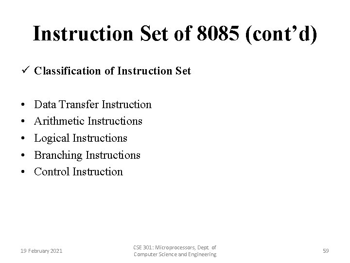
Instruction Set of 8085 (cont’d) ü Classification of Instruction Set • • • Data Transfer Instruction Arithmetic Instructions Logical Instructions Branching Instructions Control Instruction 19 February 2021 CSE 301: Microprocessors, Dept. of Computer Science and Engineering 59

Instruction Set of 8085 (cont’d) ü Data Transfer Instructions (cont’d) • These instructions move data between registers, or between memory and registers. • These instructions copy data from source to destination. • While copying, the contents of source are not modified. 19 February 2021 CSE 301: Microprocessors, Dept. of Computer Science and Engineering 60

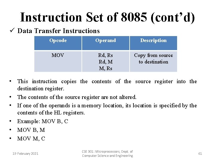
Instruction Set of 8085 (cont’d) ü Data Transfer Instructions Opcode Operand Description MOV Rd, Rs Rd, M M, Rs Copy from source to destination • This instruction copies the contents of the source register into the destination register. • The contents of the source register are not altered. • If one of the operands is a memory location, its location is specified by the contents of the HL registers. • Example: MOV B, C • MOV B, M • MOV M, C 19 February 2021 CSE 301: Microprocessors, Dept. of Computer Science and Engineering 61

Instruction Set of 8085 (cont’d) ü Arithmetic Instructions o These instructions perform the operations like: • Addition • Subtract • Increment • Decrement 19 February 2021 CSE 301: Microprocessors, Dept. of Computer Science and Engineering 62

Instruction Set of 8085 (cont’d) ü Arithmetic Instructions o Addition • Any 8 -bit number, or the contents of register, or the contents of memory location can be added to the contents of accumulator. • The result (sum) is stored in the accumulator. • No two other 8 -bit registers can be added directly. • Example: The contents of register B cannot be added directly to the contents of register C. 19 February 2021 CSE 301: Microprocessors, Dept. of Computer Science and Engineering 63

Interrupts of Intel 8085 (cont’d) ü What is interrupt? • Interrupt is a signal send by an external device to the processor, to the processor to perform a particular task or work. • Mainly in the microprocessor based system the interrupts are used for data transfer between the peripheral and the microprocessor. • When a peripheral is ready for data transfer, it interrupts the processor by sending an appropriate signal to the interrupt pin of the processor. • If the processor accepts the interrupt then the processor suspends its current activity and executes an interrupt service subroutine to complete the data transfer between the peripheral and processor. • After executing the interrupt service routine the processor resumes its current activity. 19 February 2021 CSE 301: Microprocessors, Dept. of Computer Science and Engineering 64

Interrupts of Intel 8085 (cont’d) ü Types of interrupt (cont’d) o Software interrupts • The software interrupts are program instructions. • These instructions are inserted at desired locations in a program. • While running a program, lf a software interrupt instruction is encountered, then the processor executes an interrupt service routine (ISR). • The software interrupts of 8085 are RST 0, RST 1, RST 2, RST 3, RST 4, RST 5, RST 6 and RST 7. 19 February 2021 CSE 301: Microprocessors, Dept. of Computer Science and Engineering 65

Interrupts of Intel 8085 (cont’d) ü Types of interrupt (cont’d) o Hardware interrupts • The hardware interrupts are initiated by an external device by placing an appropriate signal at the interrupt pin of the processor. • If the interrupt is accepted, then the processor executes an interrupt service routine (ISR). • The hardware interrupts of 8085 are TRAP, RST 7. 5, RST 6. 5, RST 5. 5 and INTR 19 February 2021 CSE 301: Microprocessors, Dept. of Computer Science and Engineering 66

Interrupts of Intel 8085 (cont’d) ü Types of interrupt (cont’d) o Vectored interrupts • In vectored interrupts, the processor automatically branches to the specific address in response to an interrupt. • The TRAP, RST 7. 5, RST 6. 5 and RST 5. 5 are vectored interrupts. 19 February 2021 CSE 301: Microprocessors, Dept. of Computer Science and Engineering 67

Interrupts of Intel 8085 (cont’d) ü Types of interrupt (cont’d) o Non-vectored interrupts • But in non-vectored interrupts the interrupted device should give the address of the interrupt service routine (ISR). • In vectored interrupts, the manufacturer fixes the address of the ISR to which the program control is to be transferred. • • The INTR is a non-vectored interrupt. • Hence when a device interrupts through INTR, it has to supply the address of ISR after receiving interrupt acknowledge signal. 19 February 2021 CSE 301: Microprocessors, Dept. of Computer Science and Engineering 68

Interrupts of Intel 8085 (cont’d) ü Types of interrupt (cont’d) o Maskable interrupts • Maskable Interrupts are those which can be disabled or ignored by the microprocessor. • These interrupts are either edge-triggered or level-triggered, so they can be disabled. INTR, RST 7. 5, RST 6. 5, RST 5. 5 are maskable interrupts in 8085 microprocessor. • The maskable interrupt process in the 8085 is controlled by a single flip flop inside the microprocessor. • This Interrupt Enable flip flop is controlled using the two instructions “EI” and “DI”. 19 February 2021 CSE 301: Microprocessors, Dept. of Computer Science and Engineering 69

Interrupts of Intel 8085 (cont’d) ü Types of interrupt (cont’d) o Non-maskabled interrupts • Non-Maskable Interrupts are those which cannot be disabled or ignored by microprocessor. • TRAP is a non-maskable interrupt. • The non-maskable interrupt is not affected by the value of the Interrupt Enable flip flop. 19 February 2021 CSE 301: Microprocessors, Dept. of Computer Science and Engineering 70

Interrupts of Intel 8085 (cont’d) ü Vectored interrupts o In vectored interrupts, the processor automatically branches to the specific address in response to an interrupt. o The TRAP, RST 7. 5, RST 6. 5 and RST 5. 5 are vectored interrupts ü Non-Vectored Interrupts o Non-vectored interrupts are those in which vector address is not predefined. The interrupting device gives the address of sub-routine for these interrupts. o INTR is the only non-vectored interrupt in 8085 microprocessor. 19 February 2021 CSE 301: Microprocessors, Dept. of Computer Science and Engineering 71