Agenda for today Today we will do another

- Slides: 48

Agenda for today • Today we will do another tutorial example to continue introduction to Lumerical FDTD software. – Task #1: Tune the resonance frequency of a gold nanobar using the parametric sweep feature of Lumerical FDTD. – Task #2: Calculate the Q-factor of the resonant mode • Next week: Begin discussing waveguide simulations 1

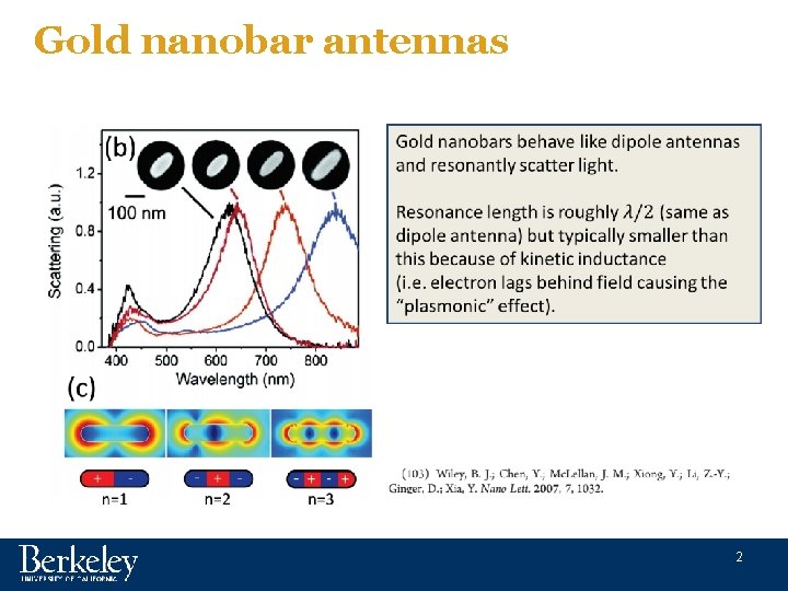
Gold nanobar antennas 2

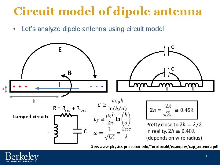
Circuit model of dipole antenna • Let’s analyze dipole antenna using circuit model C E C B a I + + + - - - L L L h R = Rrad + Rloss Lumped circuit: L C See: www. physics. princeton. edu/~mcdonald/examples/cap_antenna. pdf 3

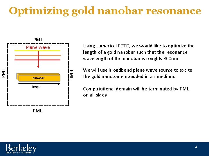
Optimizing gold nanobar resonance nanobar length Using Lumerical FDTD, we would like to optimize the length of a gold nanobar such that the resonance wavelength of the nanobar is roughly 800 nm PML PML Plane wave We will use broadband plane wave source to excite the gold nanobar embedded in air medium. Computational domain will be terminated by PML on all sides PML 4

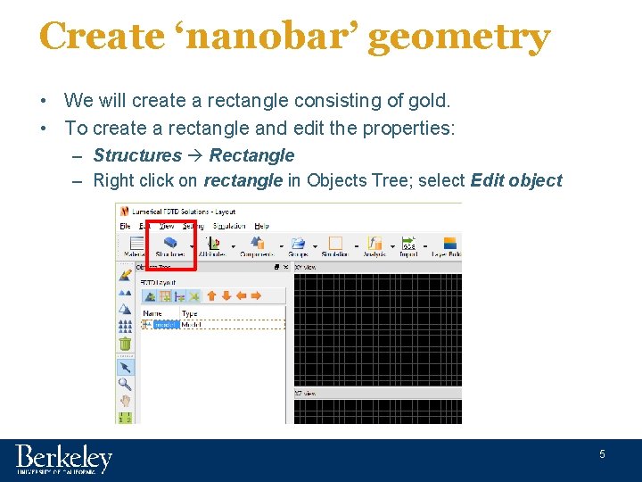
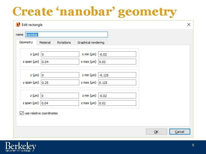
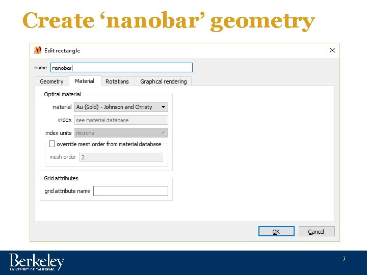
Create ‘nanobar’ geometry • We will create a rectangle consisting of gold. • To create a rectangle and edit the properties: – Structures Rectangle – Right click on rectangle in Objects Tree; select Edit object 5

Create ‘nanobar’ geometry 6

Create ‘nanobar’ geometry 7

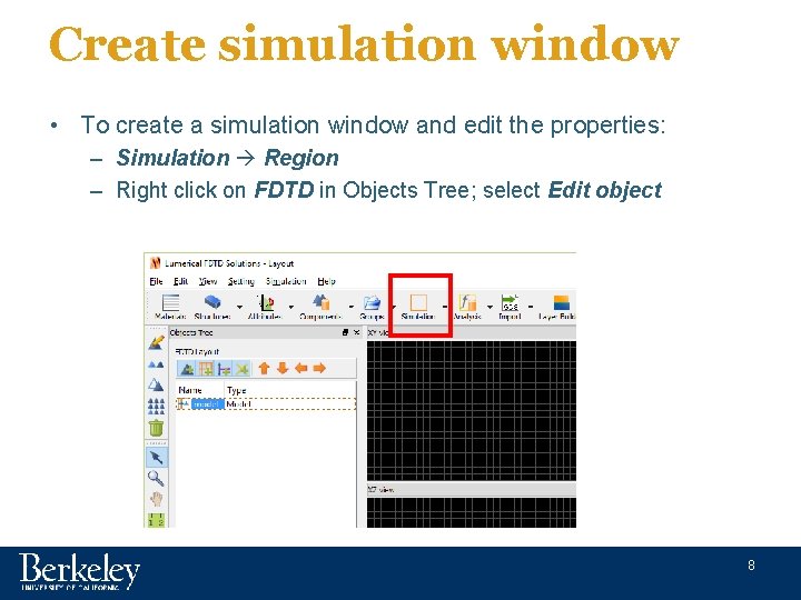
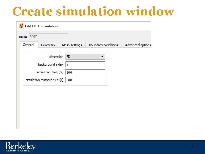
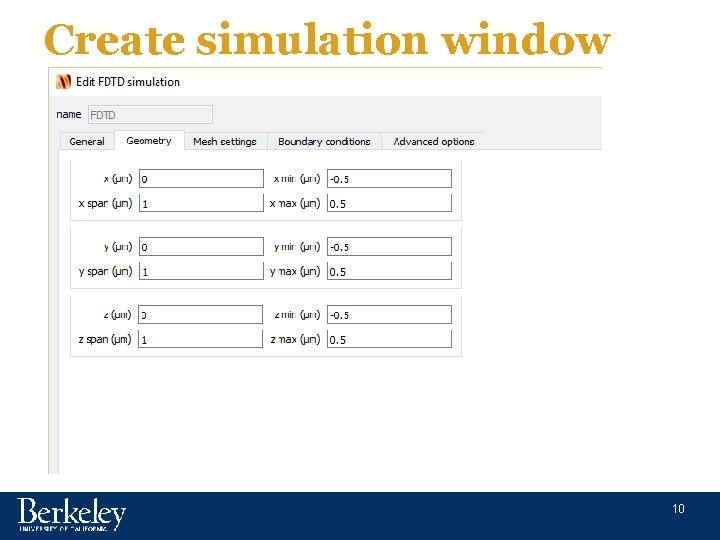
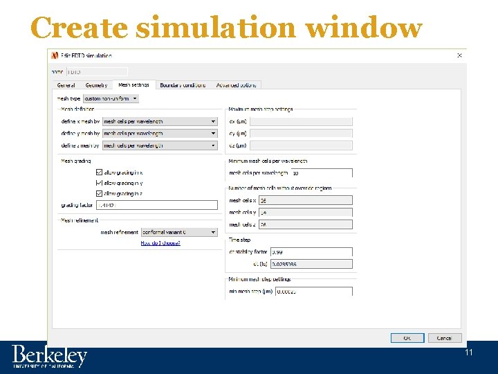
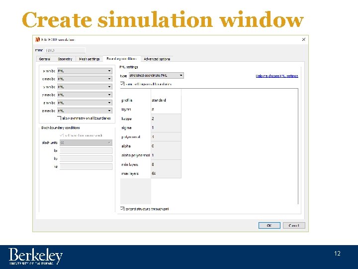
Create simulation window • To create a simulation window and edit the properties: – Simulation Region – Right click on FDTD in Objects Tree; select Edit object 8

Create simulation window 9

Create simulation window 10

Create simulation window 11

Create simulation window 12

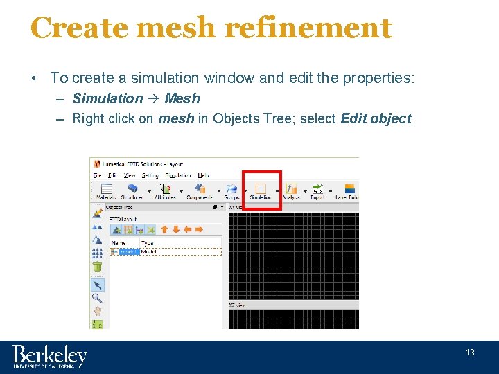
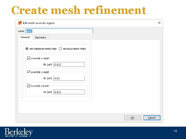
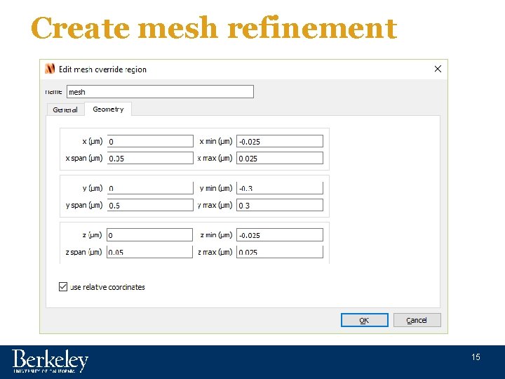
Create mesh refinement • To create a simulation window and edit the properties: – Simulation Mesh – Right click on mesh in Objects Tree; select Edit object 13

Create mesh refinement 14

Create mesh refinement 15

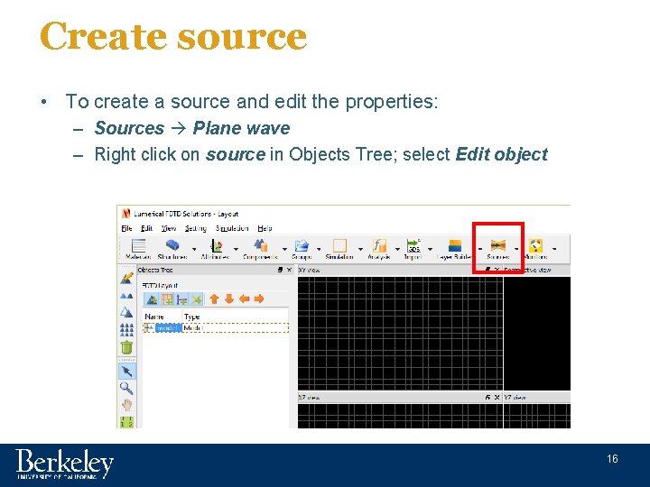
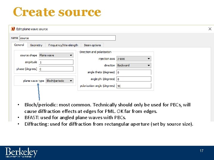
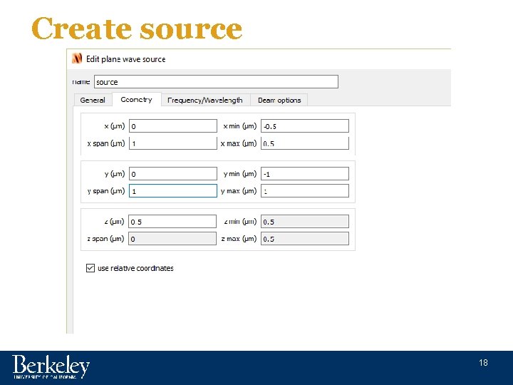
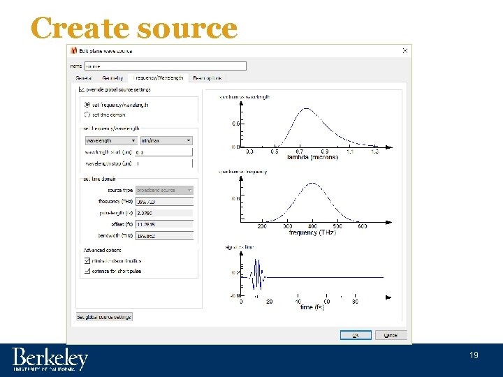
Create source • To create a source and edit the properties: – Sources Plane wave – Right click on source in Objects Tree; select Edit object 16

Create source • Bloch/periodic: most common. Technically should only be used for PBCs, will cause diffraction effects at edges for PML. OK far from edges. • BFAST: used for angled plane waves with PBCs. • Diffracting: used for diffraction from rectangular aperture (set by source size). 17

Create source 18

Create source 19

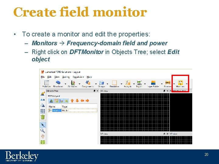
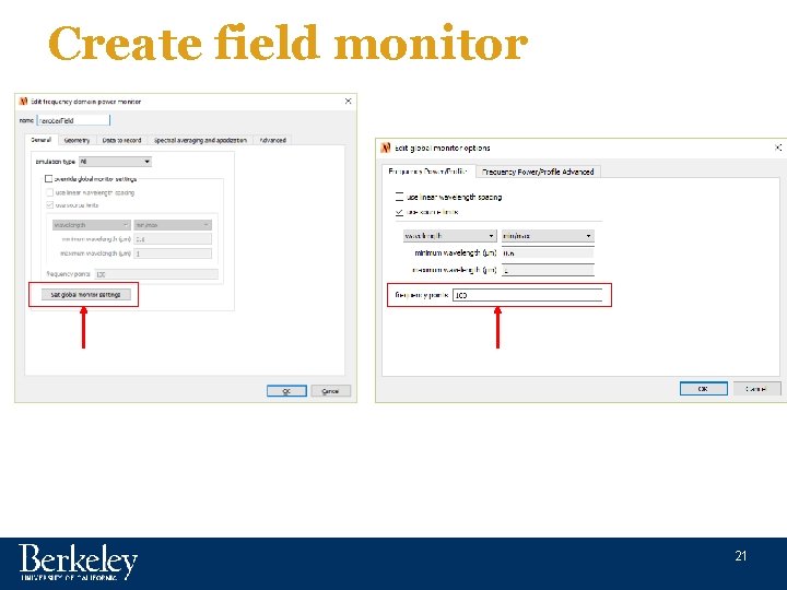
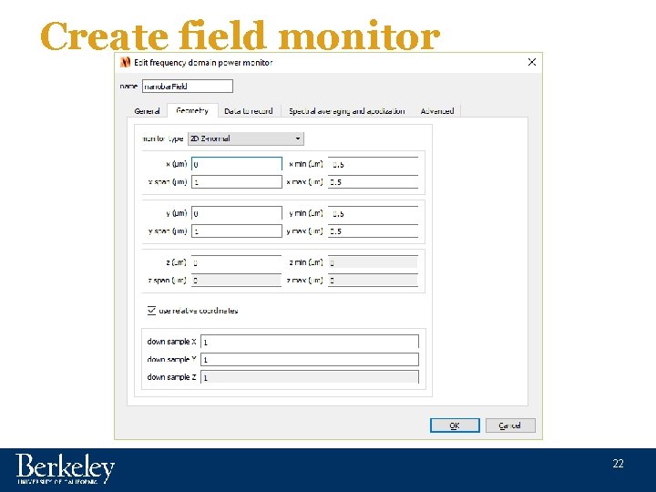
Create field monitor • To create a monitor and edit the properties: – Monitors Frequency-domain field and power – Right click on DFTMonitor in Objects Tree; select Edit object 20

Create field monitor 21

Create field monitor 22

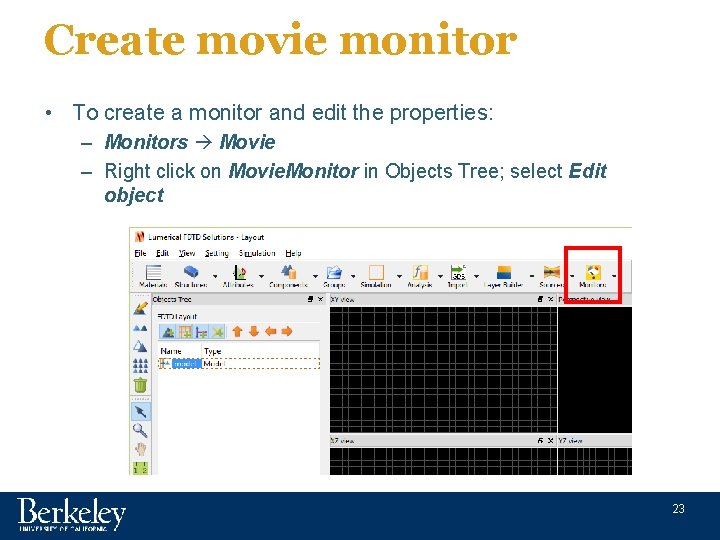
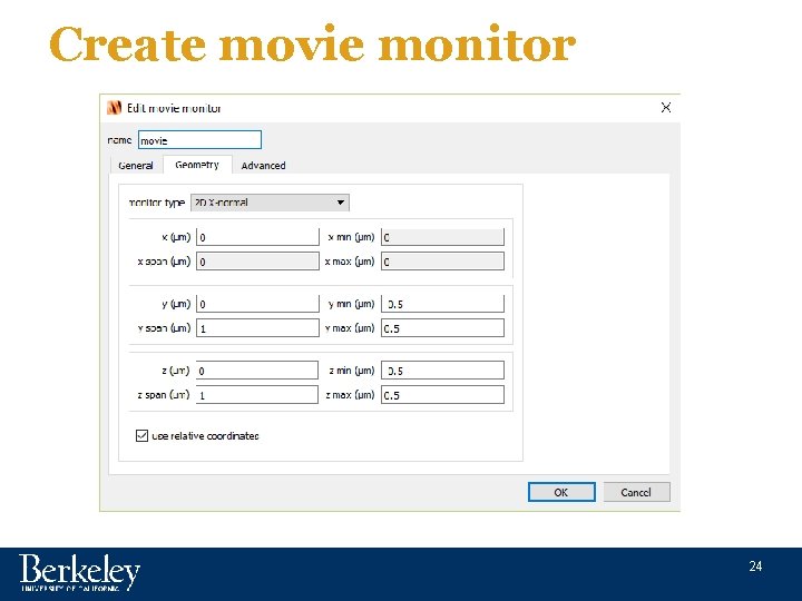
Create movie monitor • To create a monitor and edit the properties: – Monitors Movie – Right click on Movie. Monitor in Objects Tree; select Edit object 23

Create movie monitor 24

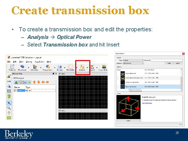
Create transmission box • To create a transmission box and edit the properties: – Analysis Optical Power – Select Transmission box and hit Insert 25

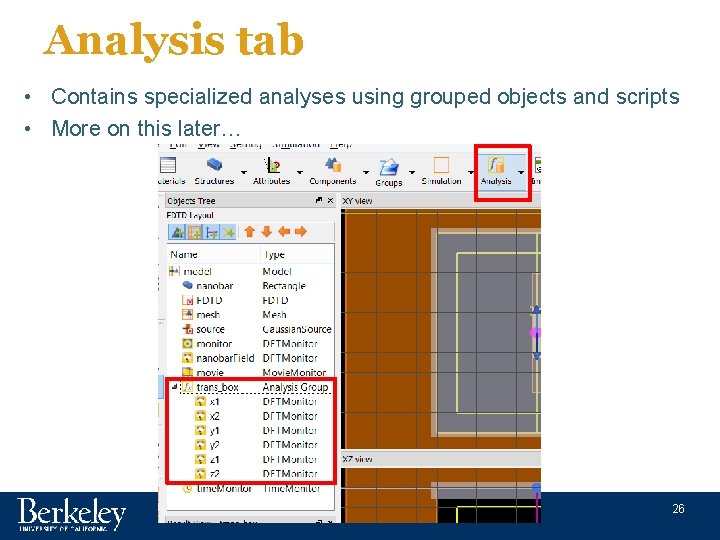
Analysis tab • Contains specialized analyses using grouped objects and scripts • More on this later… 26

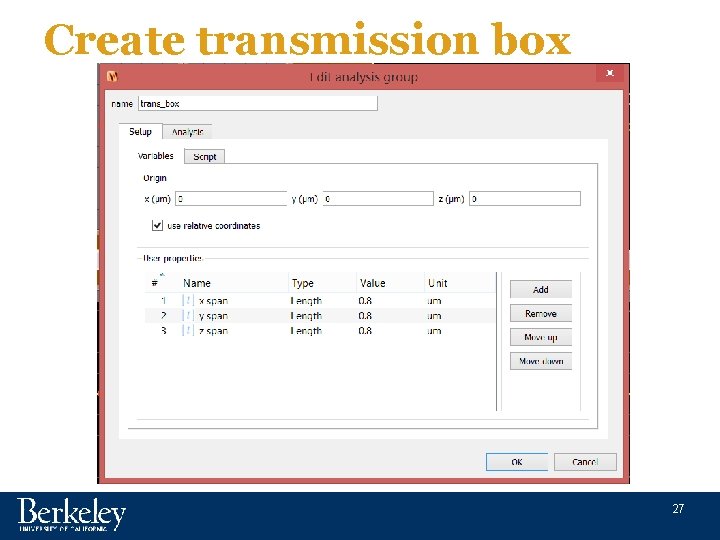
Create transmission box 27

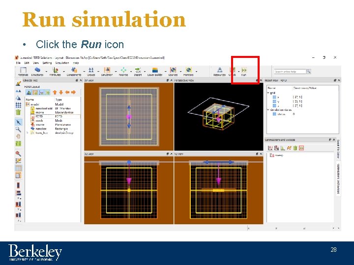
Run simulation • Click the Run icon 28

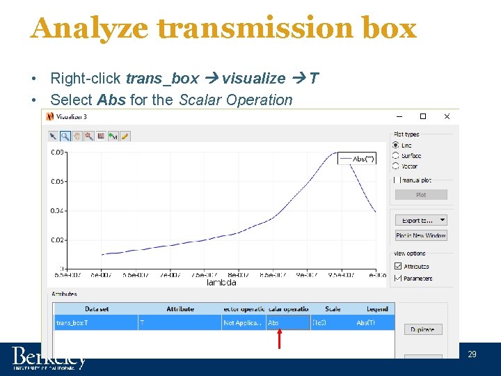
Analyze transmission box • Right-click trans_box visualize T • Select Abs for the Scalar Operation 29

Analyze transmission box • Transmission box measures net power that leaves the box. • The nanobar absorbs energy and therefore the net power is negative because of loss. • We observe resonance peak close to 950 nm. Let’s try to optimize nanobar length to push the resonance closer to 800 nm 30

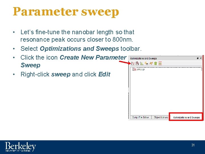
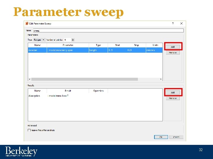
Parameter sweep • Let’s fine-tune the nanobar length so that resonance peak occurs closer to 800 nm. • Select Optimizations and Sweeps toolbar. • Click the icon Create New Parameter Sweep • Right-click sweep and click Edit 31

Parameter sweep 32

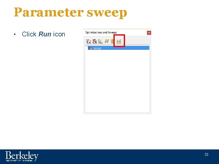
Parameter sweep • Click Run icon 33

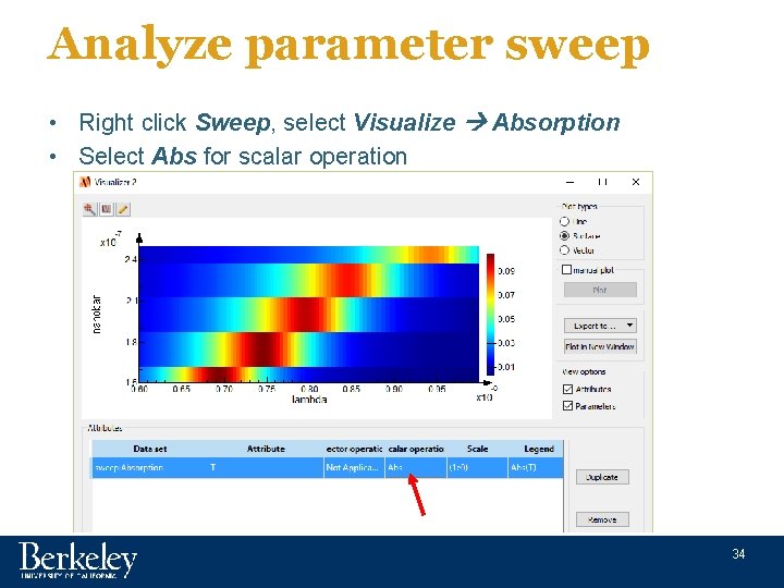
Analyze parameter sweep • Right click Sweep, select Visualize Absorption • Select Abs for scalar operation 34

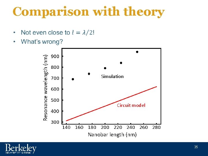
Comparison with theory Resonance wavelength (nm) • Simulation Circuit model Nanobar length (nm) 35

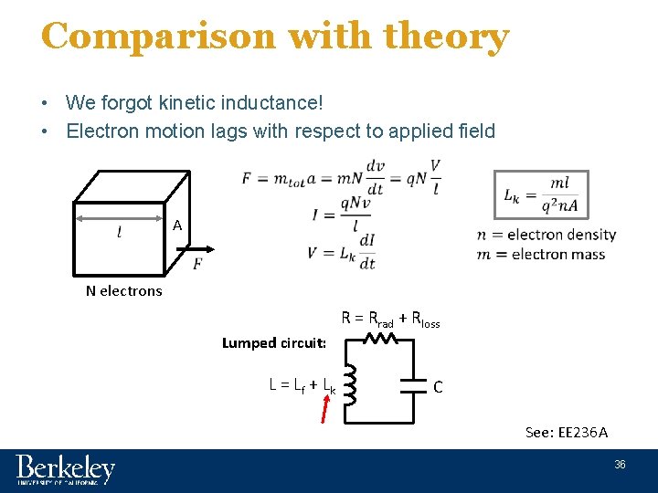
Comparison with theory • We forgot kinetic inductance! • Electron motion lags with respect to applied field A N electrons R = Rrad + Rloss Lumped circuit: L = L f + Lk C See: EE 236 A 36

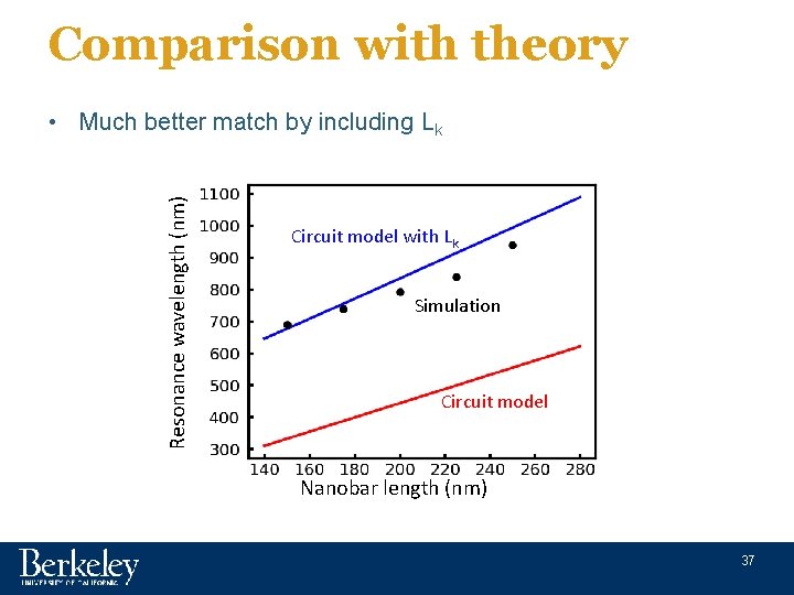
Comparison with theory Resonance wavelength (nm) • Much better match by including Lk Circuit model with Lk Simulation Circuit model Nanobar length (nm) 37

Analyze parameter sweep • 38

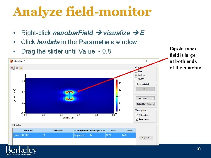
Analyze field-monitor • Right-click nanobar. Field visualize E • Click lambda in the Parameters window. • Drag the slider until Value ~ 0. 8 Dipole-mode field is large at both ends of the nanobar 39

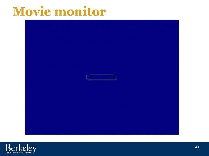
Movie monitor 40

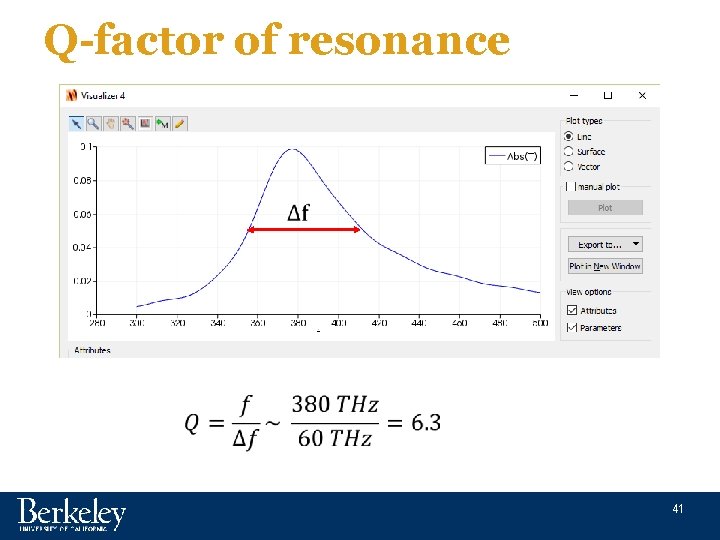
Q-factor of resonance 41

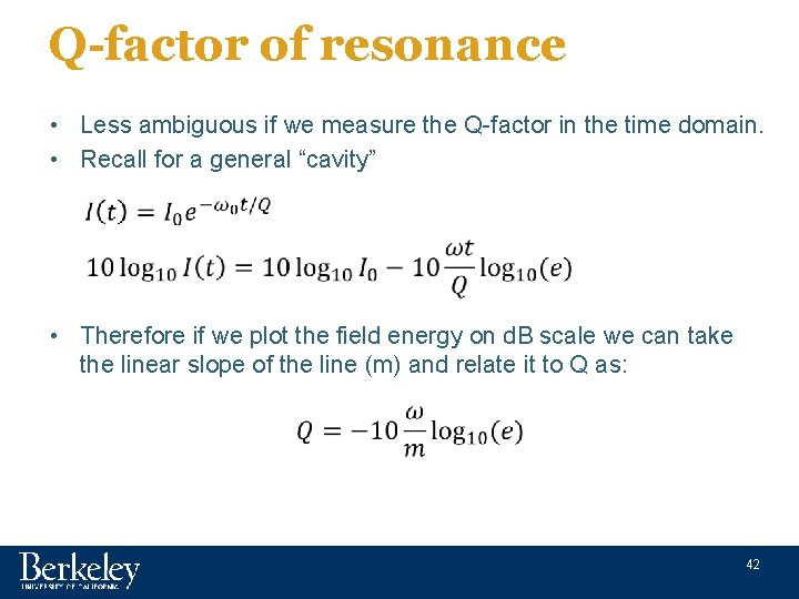
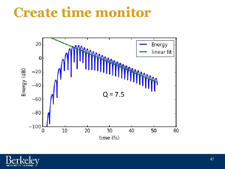
Q-factor of resonance • Less ambiguous if we measure the Q-factor in the time domain. • Recall for a general “cavity” • Therefore if we plot the field energy on d. B scale we can take the linear slope of the line (m) and relate it to Q as: 42

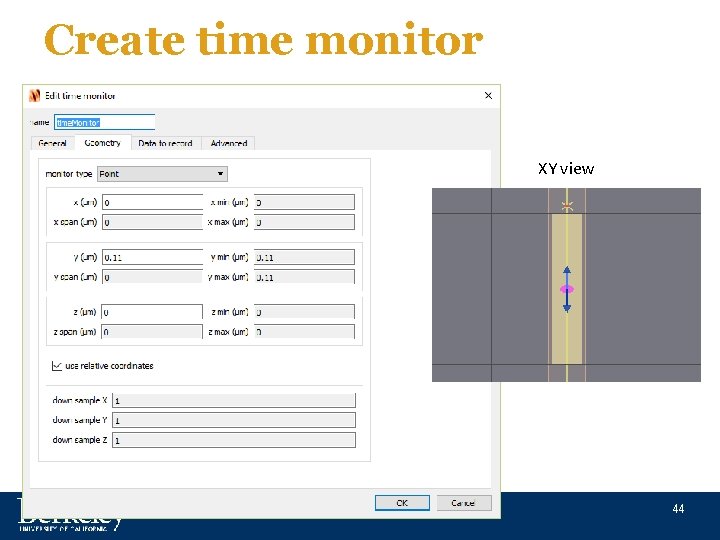
Create time monitor • To create a time monitor and edit the properties: – Monitors Field time – Right click on Time. Monitor in Objects Tree; select Edit object 43

Create time monitor XY view 44

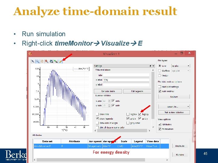
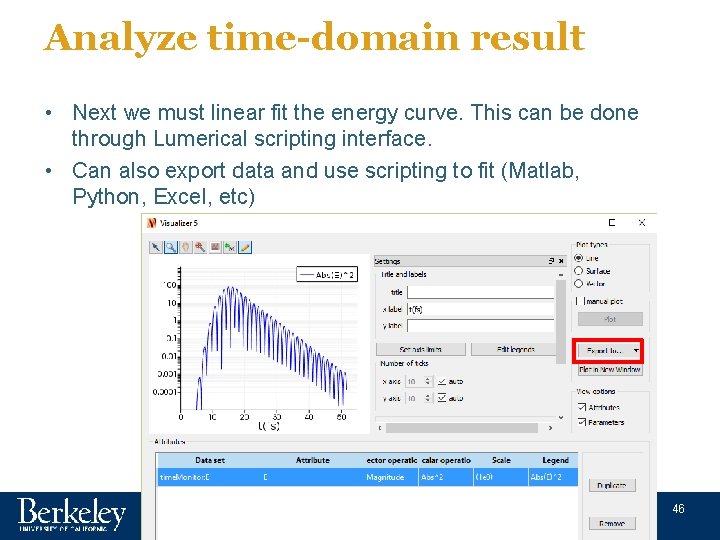
Analyze time-domain result • Run simulation • Right-click time. Monitor Visualize E For energy density 45

Analyze time-domain result • Next we must linear fit the energy curve. This can be done through Lumerical scripting interface. • Can also export data and use scripting to fit (Matlab, Python, Excel, etc) 46

Create time monitor Q = 7. 5 47

Next time • Intro to waveguides and MODE simulation 48