William Stallings Computer Organization and Architecture Chapter 4
- Slides: 71

William Stallings Computer Organization and Architecture Chapter 4 & 5 Cache Memory and Internal Memory Rev. by Luciano Gualà (2008) 4 - 1

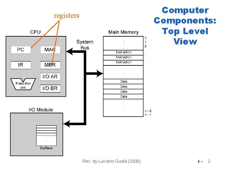
Computer Components: Top Level View registers Rev. by Luciano Gualà (2008) 4 - 2

Memory • How much ? § As much as possible • How fast ? § As fast as possible • How expensive ? § As cheap as possible • Fast memory is expensive • Large memory is expensive • The larger the memory, the slower the access Rev. by Luciano Gualà (2008) 4 - 3

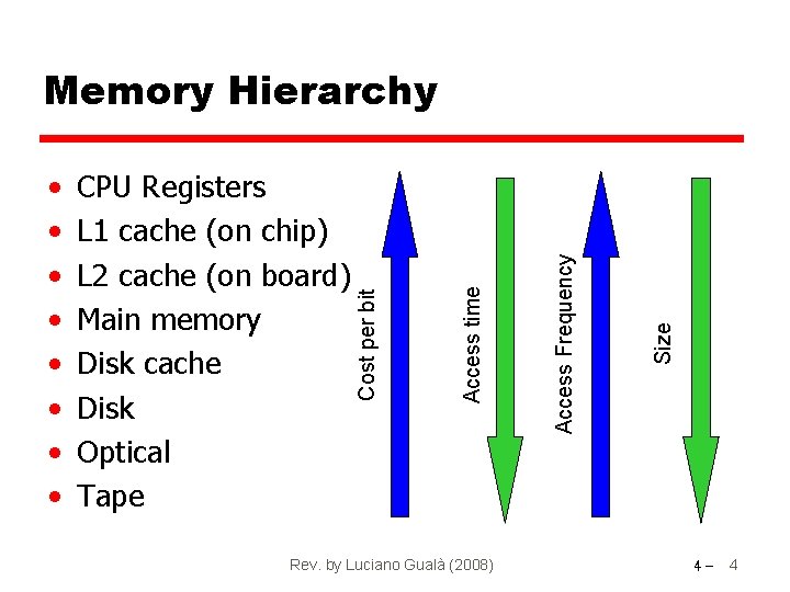
Rev. by Luciano Gualà (2008) Size Access Frequency CPU Registers L 1 cache (on chip) L 2 cache (on board) Main memory Disk cache Disk Optical Tape Access time • • Cost per bit Memory Hierarchy 4 - 4

Characteristics • • Location Capacity Unit of transfer Access method Performance Physical type Physical characteristics Organisation Rev. by Luciano Gualà (2008) 4 - 5

Location • CPU § Registers • Internal: access directly from CPU § Cache § RAM • External: access through I/O module § Disks § CD-ROM, … Rev. by Luciano Gualà (2008) 4 - 6

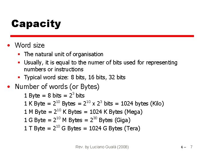
Capacity • Word size § The natural unit of organisation § Usually, it is equal to the numer of bits used for representing numbers or instructions § Typical word size: 8 bits, 16 bits, 32 bits • Number of words (or Bytes) 1 1 1 Byte = 8 bits = 23 bits K Byte = 210 Bytes = 210 x 23 bits = 1024 bytes (Kilo) M Byte = 210 K Bytes = 1024 K Bytes (Mega) G Byte = 210 M Bytes = 230 Bytes (Giga) T Byte = 210 G Bytes = 1024 G Bytes (Tera) Rev. by Luciano Gualà (2008) 4 - 7

Unit of Transfer • Number of bits can be read/written at the same time • Internal § Usually governed by data bus width § bus width may be equal to word size or (often) larger § Typical bus width: 64, 128, 256 bits • External § Usually a block which is much larger than a word • A related concept: addressable unit § Smallest location which can be uniquely addressed § Word internally § Cluster on M$ disks Rev. by Luciano Gualà (2008) 4 - 8

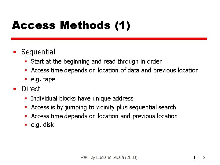
Access Methods (1) • Sequential § Start at the beginning and read through in order § Access time depends on location of data and previous location § e. g. tape • Direct § § Individual blocks have unique address Access is by jumping to vicinity plus sequential search Access time depends on location and previous location e. g. disk Rev. by Luciano Gualà (2008) 4 - 9

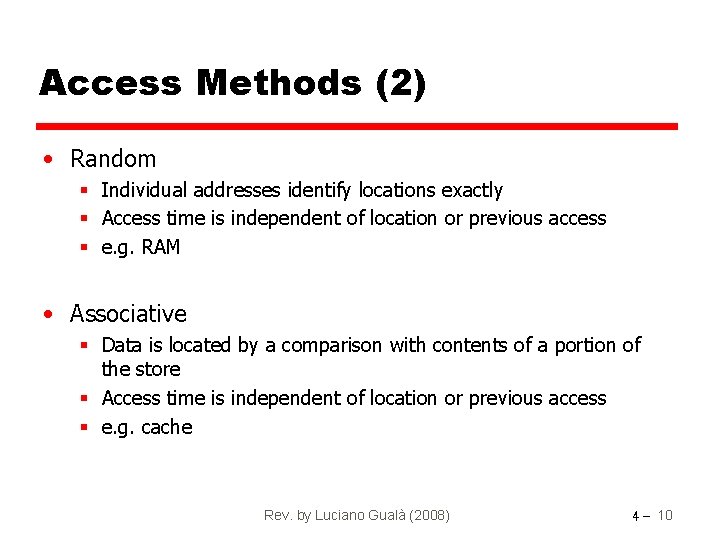
Access Methods (2) • Random § Individual addresses identify locations exactly § Access time is independent of location or previous access § e. g. RAM • Associative § Data is located by a comparison with contents of a portion of the store § Access time is independent of location or previous access § e. g. cache Rev. by Luciano Gualà (2008) 4 - 10

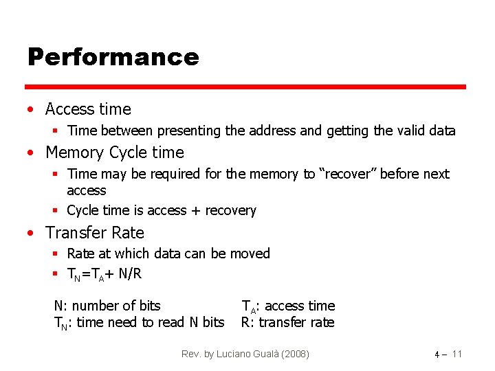
Performance • Access time § Time between presenting the address and getting the valid data • Memory Cycle time § Time may be required for the memory to “recover” before next access § Cycle time is access + recovery • Transfer Rate § Rate at which data can be moved § TN=TA+ N/R N: number of bits TN: time need to read N bits TA: access time R: transfer rate Rev. by Luciano Gualà (2008) 4 - 11

Physical Types • Semiconductor § RAM, ROM, EPROM, Cache • Magnetic § Disk & Tape • Optical § CD & DVD • Others § … Rev. by Luciano Gualà (2008) 4 - 12

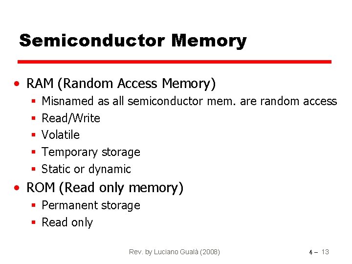
Semiconductor Memory • RAM (Random Access Memory) § § § Misnamed as all semiconductor mem. are random access Read/Write Volatile Temporary storage Static or dynamic • ROM (Read only memory) § Permanent storage § Read only Rev. by Luciano Gualà (2008) 4 - 13

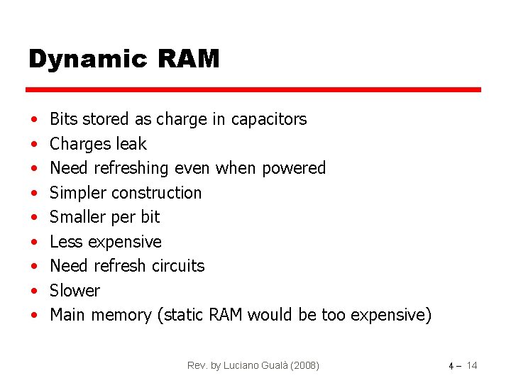
Dynamic RAM • • • Bits stored as charge in capacitors Charges leak Need refreshing even when powered Simpler construction Smaller per bit Less expensive Need refresh circuits Slower Main memory (static RAM would be too expensive) Rev. by Luciano Gualà (2008) 4 - 14

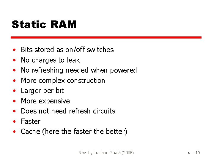
Static RAM • • • Bits stored as on/off switches No charges to leak No refreshing needed when powered More complex construction Larger per bit More expensive Does not need refresh circuits Faster Cache (here the faster the better) Rev. by Luciano Gualà (2008) 4 - 15

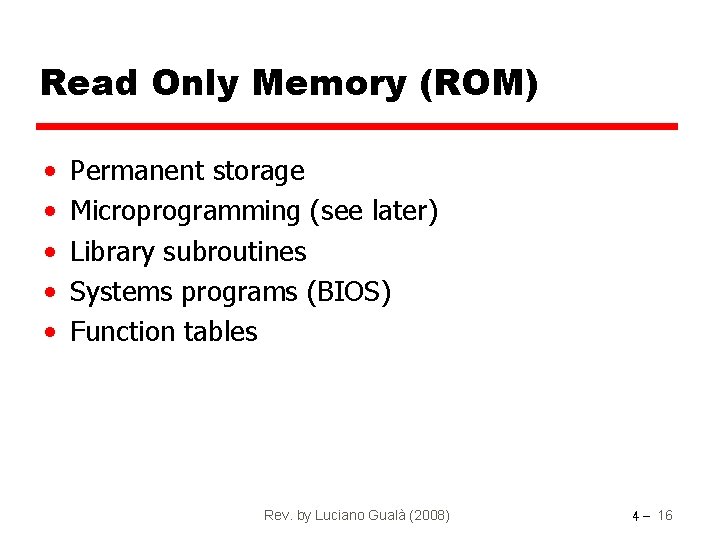
Read Only Memory (ROM) • • • Permanent storage Microprogramming (see later) Library subroutines Systems programs (BIOS) Function tables Rev. by Luciano Gualà (2008) 4 - 16

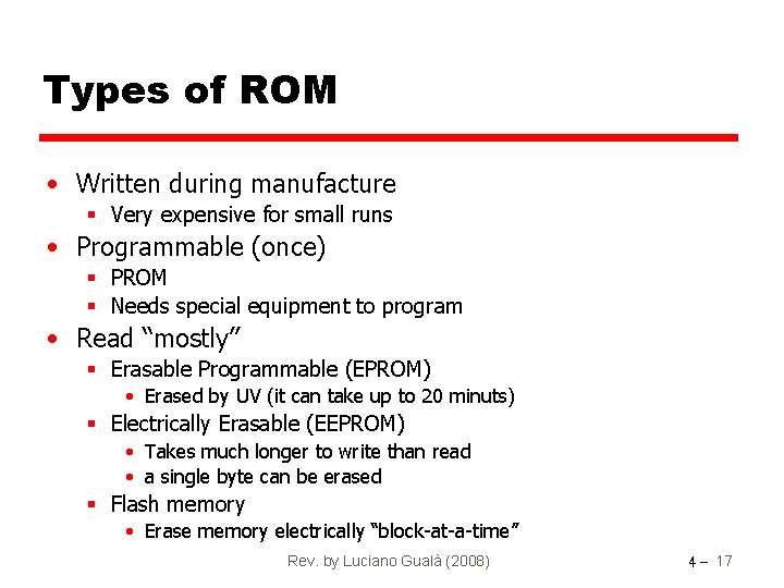
Types of ROM • Written during manufacture § Very expensive for small runs • Programmable (once) § PROM § Needs special equipment to program • Read “mostly” § Erasable Programmable (EPROM) • Erased by UV (it can take up to 20 minuts) § Electrically Erasable (EEPROM) • Takes much longer to write than read • a single byte can be erased § Flash memory • Erase memory electrically “block-at-a-time” Rev. by Luciano Gualà (2008) 4 - 17

Physical Characteristics • • Decay (refresh time) Volatility (needs power source) Erasable Power consumption Rev. by Luciano Gualà (2008) 4 - 18

Organisation • Physical arrangement of bits into words • Not always obvious § e. g. interleaved Rev. by Luciano Gualà (2008) 4 - 19

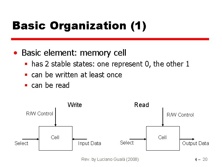
Basic Organization (1) • Basic element: memory cell § has 2 stable states: one represent 0, the other 1 § can be written at least once § can be read Write Read R/W Control Cell Select Input Data Select Rev. by Luciano Gualà (2008) Cell Output Data 4 - 20

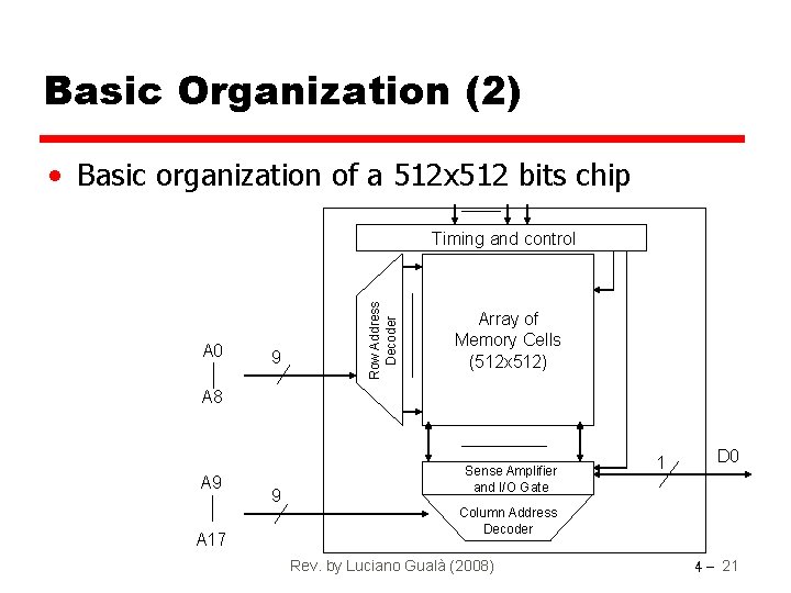
Basic Organization (2) • Basic organization of a 512 x 512 bits chip A 0 9 Row Address Decoder Timing and control Array of Memory Cells (512 x 512) A 8 A 9 A 17 9 Sense Amplifier and I/O Gate 1 D 0 Column Address Decoder Rev. by Luciano Gualà (2008) 4 - 21

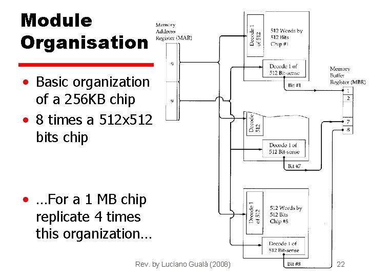
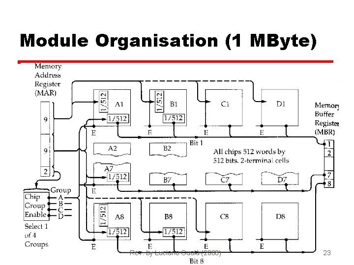
Module Organisation • Basic organization of a 256 KB chip • 8 times a 512 x 512 bits chip • …For a 1 MB chip replicate 4 times this organization… Rev. by Luciano Gualà (2008) 4 - 22

Module Organisation (1 MByte) Rev. by Luciano Gualà (2008) 4 - 23

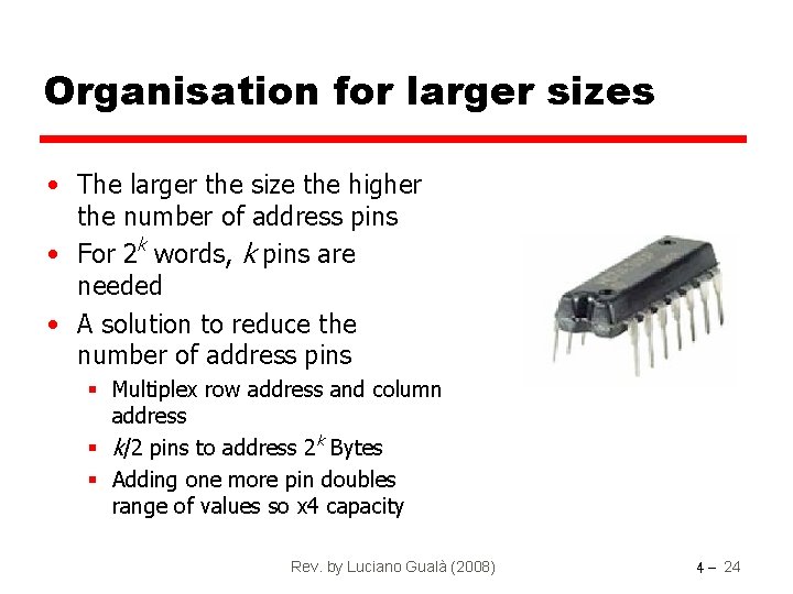
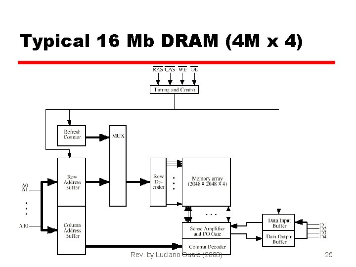
Organisation for larger sizes • The larger the size the higher the number of address pins • For 2 k words, k pins are needed • A solution to reduce the number of address pins § Multiplex row address and column address § k/2 pins to address 2 k Bytes § Adding one more pin doubles range of values so x 4 capacity Rev. by Luciano Gualà (2008) 4 - 24

Typical 16 Mb DRAM (4 M x 4) X X Rev. by Luciano Gualà (2008) 4 - 25

Refreshing (Dynamic RAM) • • • Refresh circuit included on chip Disable chip Count through rows Read & Write back Takes time Slows down apparent performance Rev. by Luciano Gualà (2008) 4 - 26

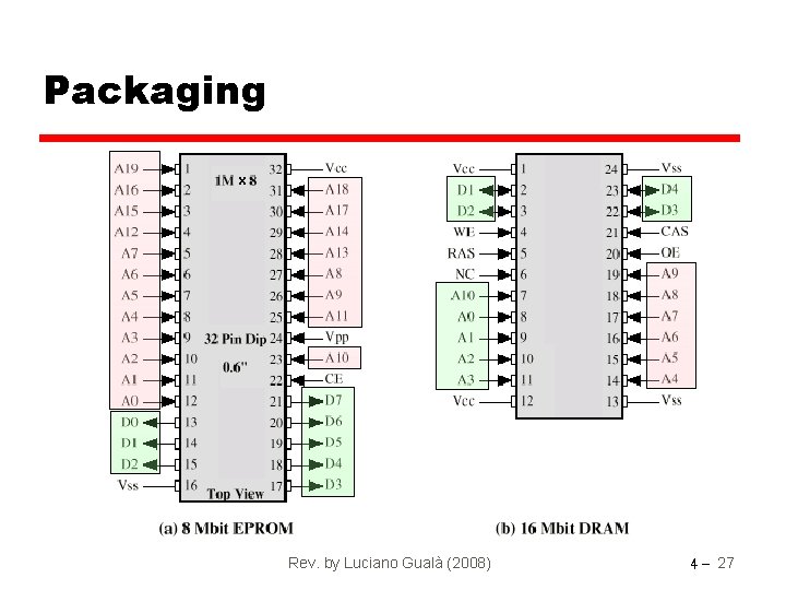
Packaging X Rev. by Luciano Gualà (2008) 4 - 27

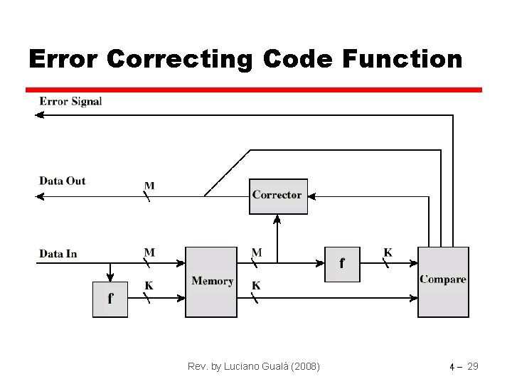
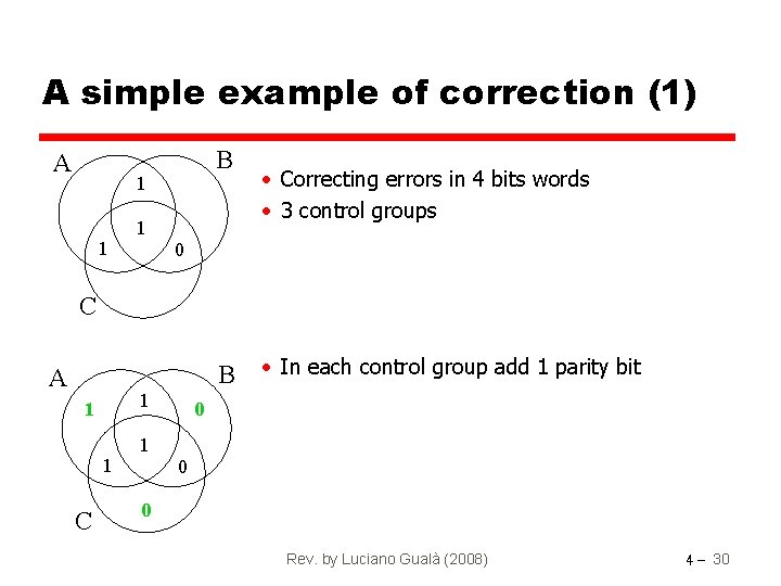
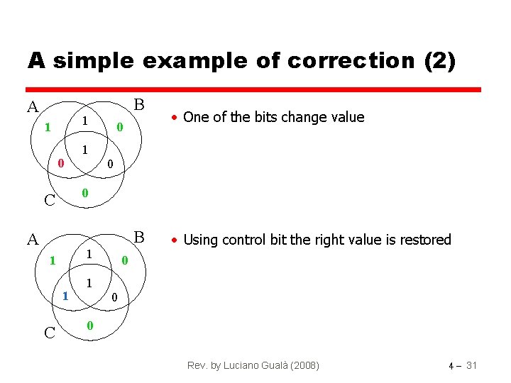
Error Correction • Hard Failure § Permanent defect • Soft Error § Random, non-destructive § No permanent damage to memory • Detected using Hamming error correcting code § it is able to detect and correct 1 -bit errors Rev. by Luciano Gualà (2008) 4 - 28

Error Correcting Code Function Rev. by Luciano Gualà (2008) 4 - 29

A simple example of correction (1) A B 1 1 1 • Correcting errors in 4 bits words • 3 control groups 0 C B A 1 1 1 C 1 • In each control group add 1 parity bit 0 0 0 Rev. by Luciano Gualà (2008) 4 - 30

A simple example of correction (2) A B 1 1 0 0 0 C B A 1 1 1 C • One of the bits change value 1 • Using control bit the right value is restored 0 0 0 Rev. by Luciano Gualà (2008) 4 - 31

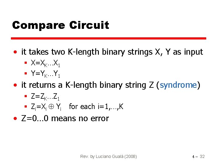
Compare Circuit • it takes two K-length binary strings X, Y as input § X=XK…X 1 § Y=YK…Y 1 • it returns a K-length binary string Z (syndrome) § Z=ZK…Z 1 § Zi=Xi Yi for each i=1, …, K • Z=0… 0 means no error Rev. by Luciano Gualà (2008) 4 - 32

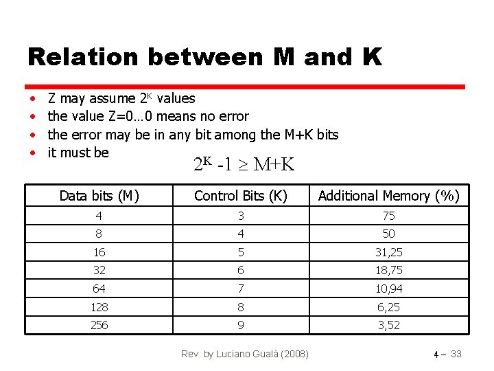
Relation between M and K • • Z may assume 2 K values the value Z=0… 0 means no error the error may be in any bit among the M+K bits it must be 2 K -1 M+K Data bits (M) Control Bits (K) Additional Memory (%) 4 3 75 8 4 50 16 5 31, 25 32 6 18, 75 64 7 10, 94 128 8 6, 25 256 9 3, 52 Rev. by Luciano Gualà (2008) 4 - 33

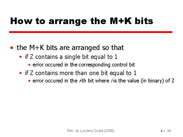
How to arrange the M+K bits • the M+K bits are arranged so that § if Z contains a single bit equal to 1 • error occured in the corresponding control bit § if Z contains more than one bit equal to 1 • error occured in the i-th bit where i is the value (in binary) of Z Rev. by Luciano Gualà (2008) 4 - 34

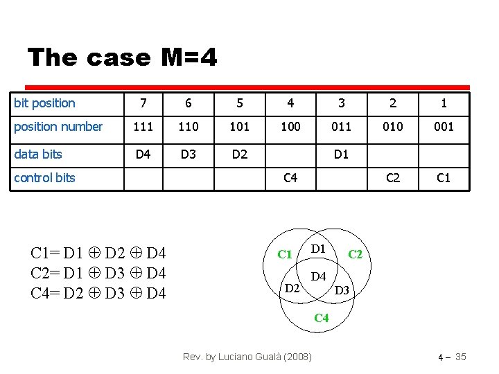
The case M=4 bit position 7 6 5 4 3 2 1 position number 111 110 101 100 011 010 001 data bits D 4 D 3 D 2 C 1 control bits C 1= D 1 D 2 D 4 C 2= D 1 D 3 D 4 C 4= D 2 D 3 D 4 D 1 C 4 C 1 D 2 D 1 D 4 C 2 D 3 C 4 Rev. by Luciano Gualà (2008) 4 - 35

Exercise • Design a Hamming error correcting code for bit words • See the textbook for the solution Rev. by Luciano Gualà (2008) 8 - 4 - 36

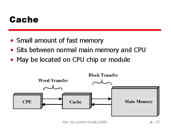
Cache • Small amount of fast memory • Sits between normal main memory and CPU • May be located on CPU chip or module Rev. by Luciano Gualà (2008) 4 - 37

Cache operation - overview • • CPU requests contents of memory location Check cache for this data If present (hit), get from cache (fast) If not present (miss), read required block from main memory to cache • Then deliver from cache to CPU Rev. by Luciano Gualà (2008) 4 - 38

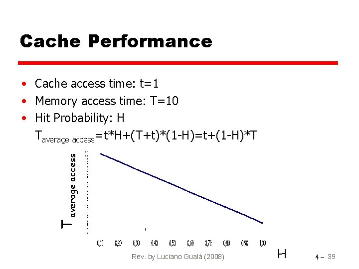
Cache Performance T average access • Cache access time: t=1 • Memory access time: T=10 • Hit Probability: H Taverage access=t*H+(T+t)*(1 -H)=t+(1 -H)*T Rev. by Luciano Gualà (2008) H 4 - 39

Locality of Reference (Denning’ 68) • Spatial Locality § Memory cells physically close to those just accessed tend to be accessed • Temporal Locality § During the course of the execution of a program, all accesses to the same memory cells tend to close in time • e. g. loops, arrays Rev. by Luciano Gualà (2008) 4 - 40

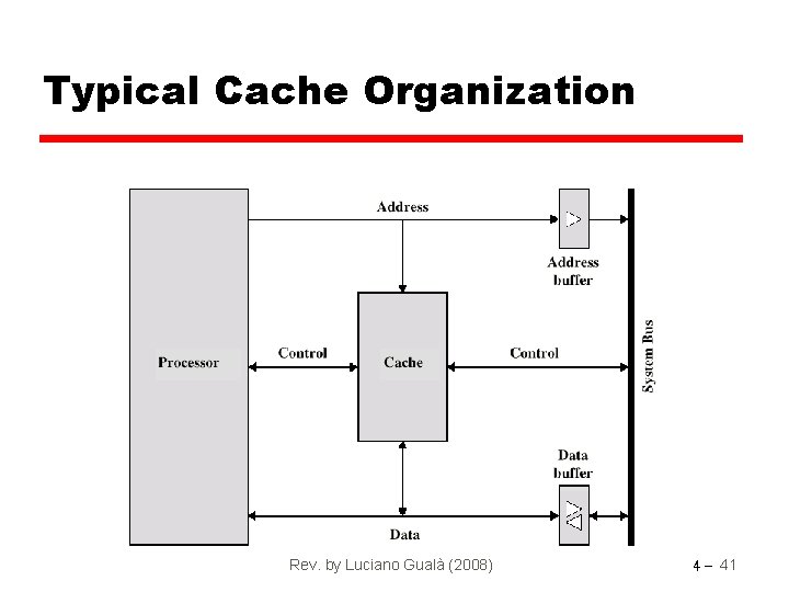
Typical Cache Organization Rev. by Luciano Gualà (2008) 4 - 41

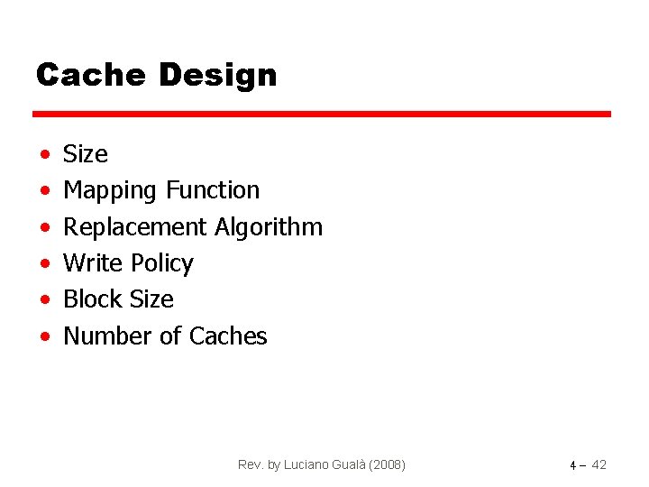
Cache Design • • • Size Mapping Function Replacement Algorithm Write Policy Block Size Number of Caches Rev. by Luciano Gualà (2008) 4 - 42

Size does matter • Cost § More cache is expensive • Speed § More cache is faster (up to a point) § Checking cache for data takes time Rev. by Luciano Gualà (2008) 4 - 43

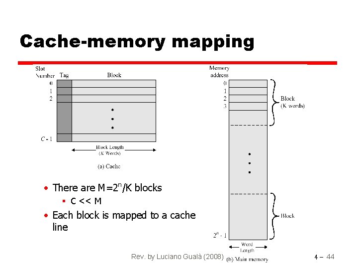
Cache-memory mapping • There are M=2 n/K blocks § C << M • Each block is mapped to a cache line Rev. by Luciano Gualà (2008) 4 - 44

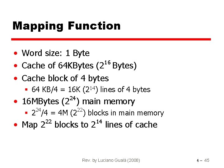
Mapping Function • Word size: 1 Byte 16 • Cache of 64 KBytes (2 Bytes) • Cache block of 4 bytes § 64 KB/4 = 16 K (214) lines of 4 bytes • 16 MBytes (224) main memory § 224/4 = 4 M (222) blocks in main memory • Map 222 blocks to 214 lines of cache Rev. by Luciano Gualà (2008) 4 - 45

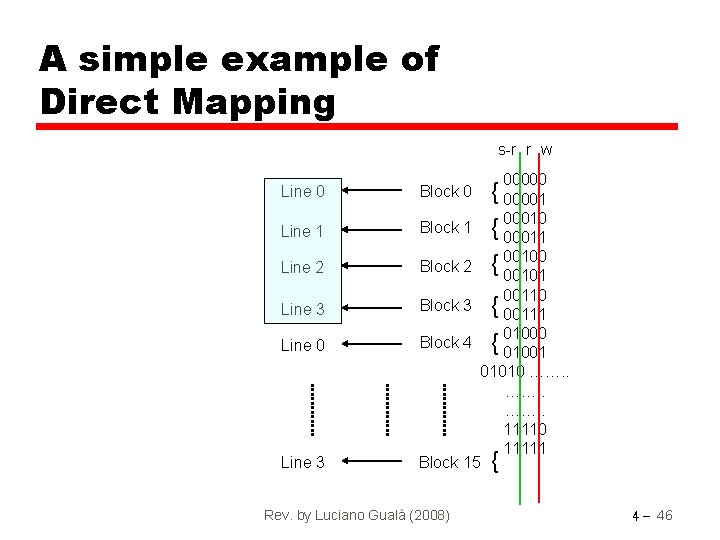
A simple example of Direct Mapping s-r r w 00000 { 00001 { 00010 00011 { 00100 00101 Line 0 Block 0 Line 1 Block 1 Line 2 Block 2 Line 3 Block 3 { 00111 Line 0 Block 4 { 01000 01001 Line 3 01010 ……. . 11110 11111 { Block 15 Rev. by Luciano Gualà (2008) 00110 4 - 46

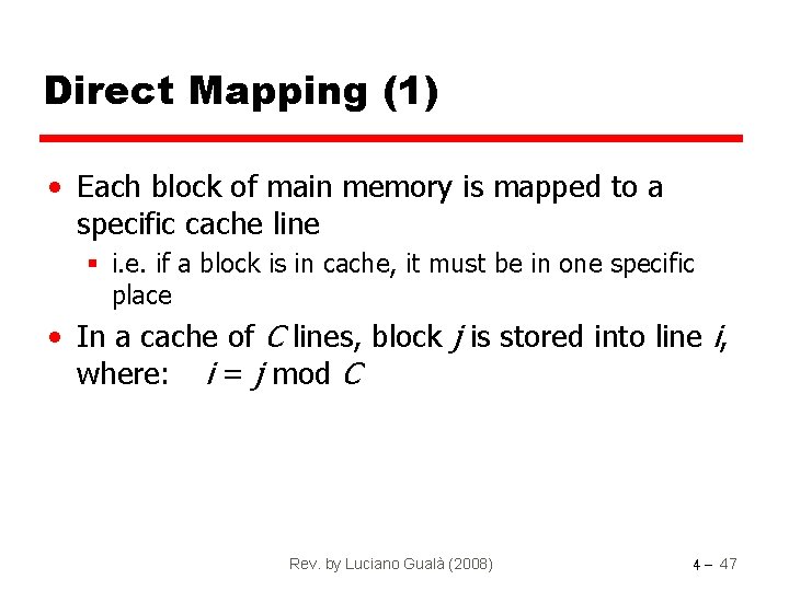
Direct Mapping (1) • Each block of main memory is mapped to a specific cache line § i. e. if a block is in cache, it must be in one specific place • In a cache of C lines, block j is stored into line i, where: i = j mod C Rev. by Luciano Gualà (2008) 4 - 47

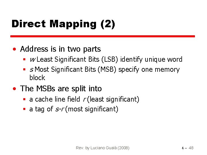
Direct Mapping (2) • Address is in two parts § w Least Significant Bits (LSB) identify unique word § s Most Significant Bits (MSB) specify one memory block • The MSBs are split into § a cache line field r (least significant) § a tag of s-r (most significant) Rev. by Luciano Gualà (2008) 4 - 48

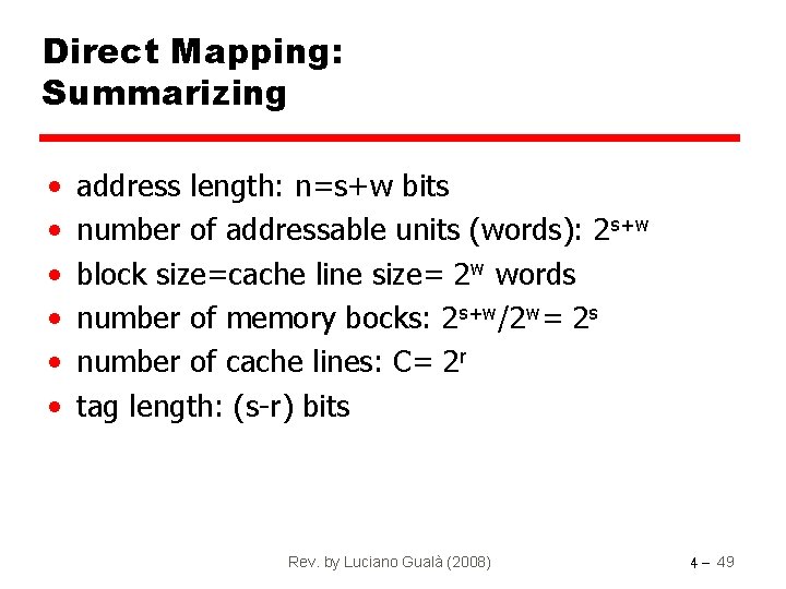
Direct Mapping: Summarizing • • • address length: n=s+w bits number of addressable units (words): 2 s+w block size=cache line size= 2 w words number of memory bocks: 2 s+w/2 w= 2 s number of cache lines: C= 2 r tag length: (s-r) bits Rev. by Luciano Gualà (2008) 4 - 49

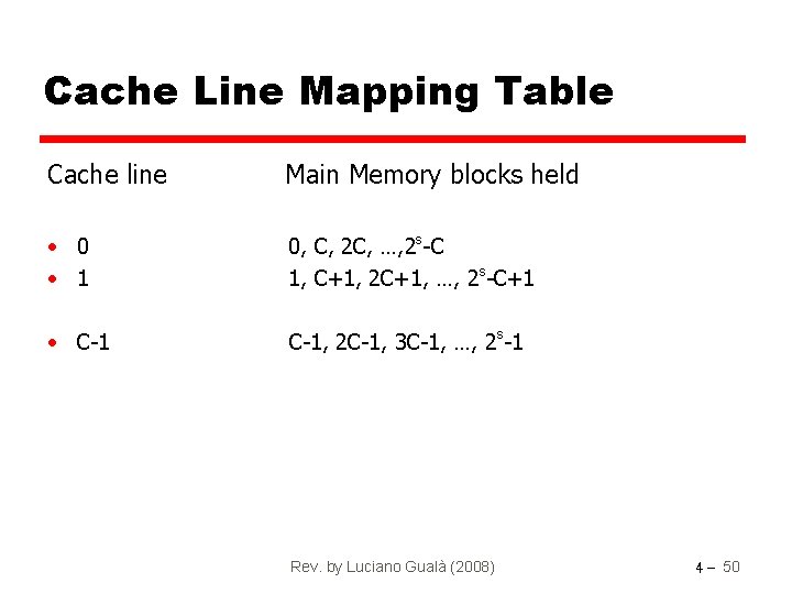
Cache Line Mapping Table Cache line Main Memory blocks held • 0 • 1 0, C, 2 C, …, 2 s-C 1, C+1, 2 C+1, …, 2 s-C+1 • C-1, 2 C-1, 3 C-1, …, 2 s-1 Rev. by Luciano Gualà (2008) 4 - 50

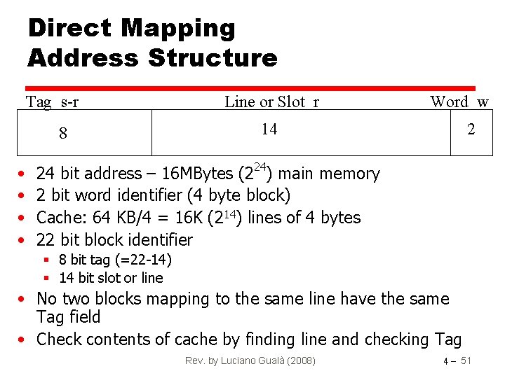
Direct Mapping Address Structure Tag s-r 8 • • Line or Slot r Word w 14 2 24 bit address – 16 MBytes (224) main memory 2 bit word identifier (4 byte block) Cache: 64 KB/4 = 16 K (214) lines of 4 bytes 22 bit block identifier § 8 bit tag (=22 -14) § 14 bit slot or line • No two blocks mapping to the same line have the same Tag field • Check contents of cache by finding line and checking Tag Rev. by Luciano Gualà (2008) 4 - 51

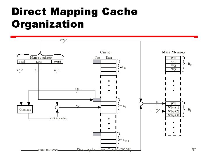
Direct Mapping Cache Organization Rev. by Luciano Gualà (2008) 4 - 52

Direct Mapping pros & cons • Simple • Inexpensive • Fixed location for given block § If a program repeatedly accesses 2 distinct blocks that are mapped to the same line, cache misses are very high (thrashing) Rev. by Luciano Gualà (2008) 4 - 53

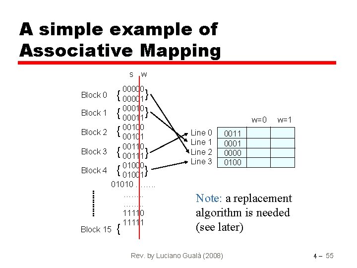
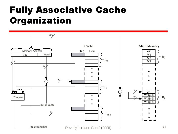
Associative Mapping • A main memory block can load into any line of cache • Memory address is interpreted as tag and word • Tag uniquely identifies block of memory • Every line’s tag is examined for a match • Cache searching gets expensive Rev. by Luciano Gualà (2008) 4 - 54

A simple example of Associative Mapping s Block 0 Block 1 Block 2 w 00000 { 00001} } { 00010 00011 { 00100 00101 00110 Block 3 { 00111 } Block 4 { 01000 01001} 01010 ……. . 11110 11111 { Block 15 w=0 Line 1 Line 2 Line 3 w=1 0011 0000 0100 Note: a replacement algorithm is needed (see later) Rev. by Luciano Gualà (2008) 4 - 55

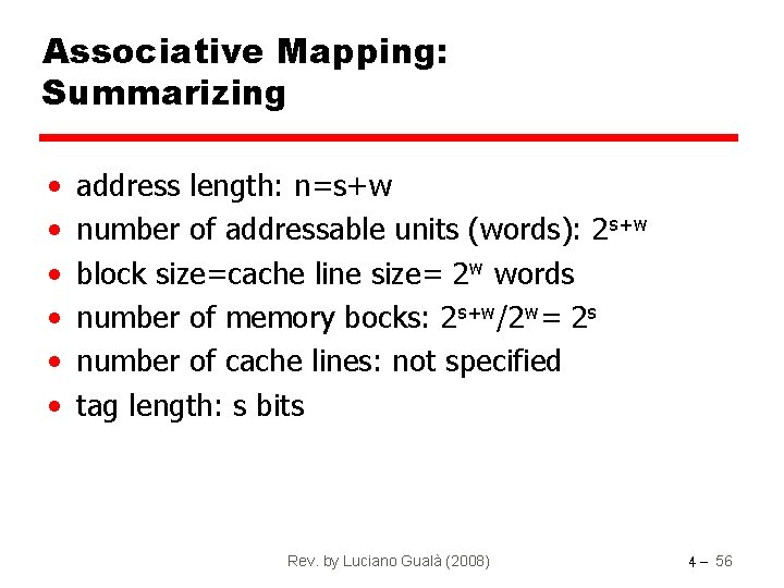
Associative Mapping: Summarizing • • • address length: n=s+w number of addressable units (words): 2 s+w block size=cache line size= 2 w words number of memory bocks: 2 s+w/2 w= 2 s number of cache lines: not specified tag length: s bits Rev. by Luciano Gualà (2008) 4 - 56

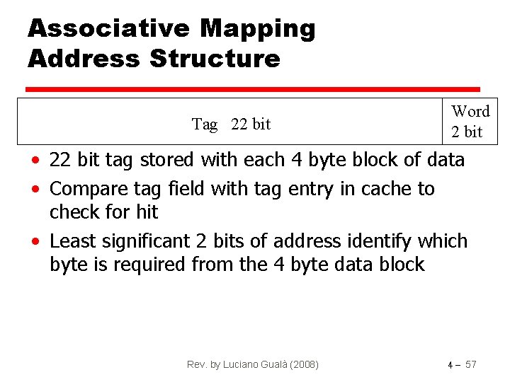
Associative Mapping Address Structure Tag 22 bit Word 2 bit • 22 bit tag stored with each 4 byte block of data • Compare tag field with tag entry in cache to check for hit • Least significant 2 bits of address identify which byte is required from the 4 byte data block Rev. by Luciano Gualà (2008) 4 - 57

Fully Associative Cache Organization Rev. by Luciano Gualà (2008) 4 - 58

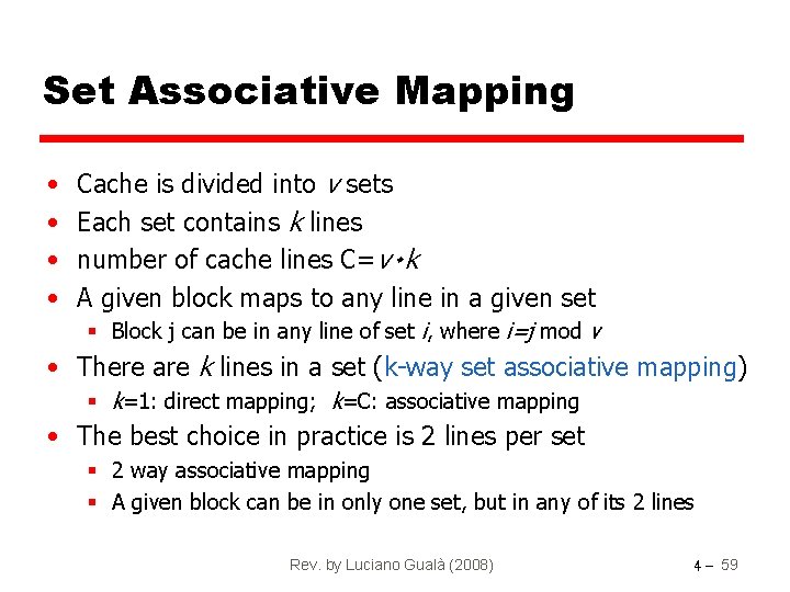
Set Associative Mapping • • Cache is divided into v sets Each set contains k lines number of cache lines C=v۰ k A given block maps to any line in a given set § Block j can be in any line of set i, where i=j mod v • There are k lines in a set (k-way set associative mapping) § k=1: direct mapping; k=C: associative mapping • The best choice in practice is 2 lines per set § 2 way associative mapping § A given block can be in only one set, but in any of its 2 lines Rev. by Luciano Gualà (2008) 4 - 59

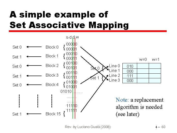
A simple example of Set Associative Mapping s-d d w 00000 { 00001 { 00010 00011 { 00100 00101 Set 0 Block 0 Set 1 Block 1 Set 0 Block 2 Set 1 Block 3 { 00111 Set 0 Block 4 { 01000 01001 Set 1 01010 ……. . 11110 11111 { Block 15 w=0 Set 0 { Set 1 { 00110 Line 1 Line 2 Line 3 Rev. by Luciano Gualà (2008) w=1 010 000 111 000 Note: a replacement algorithm is needed (see later) 4 - 60

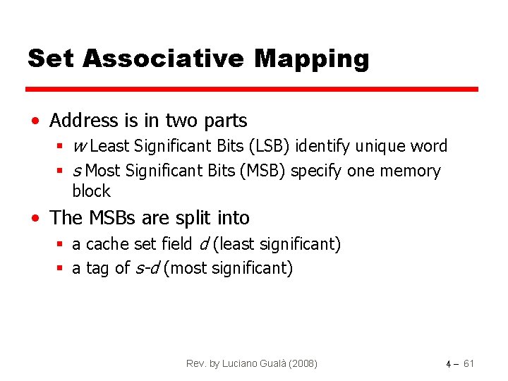
Set Associative Mapping • Address is in two parts § w Least Significant Bits (LSB) identify unique word § s Most Significant Bits (MSB) specify one memory block • The MSBs are split into § a cache set field d (least significant) § a tag of s-d (most significant) Rev. by Luciano Gualà (2008) 4 - 61

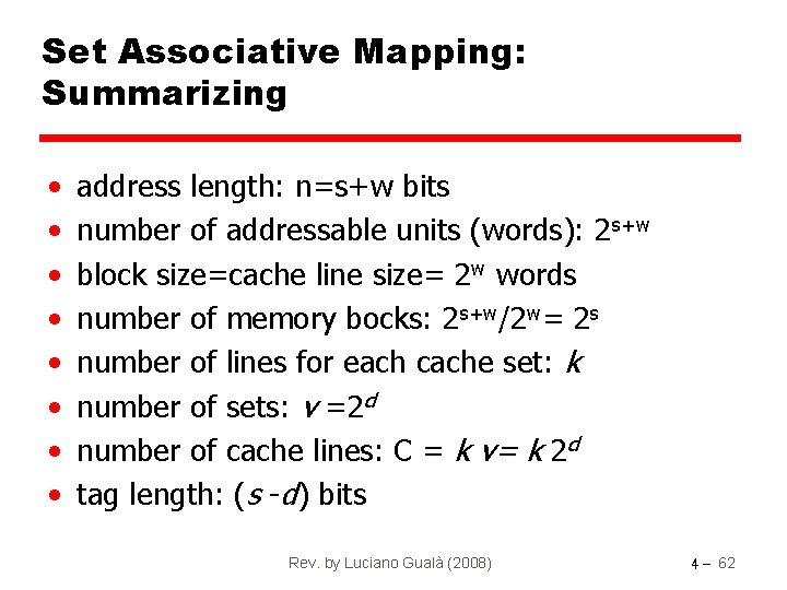
Set Associative Mapping: Summarizing • • address length: n=s+w bits number of addressable units (words): 2 s+w block size=cache line size= 2 w words number of memory bocks: 2 s+w/2 w= 2 s number of lines for each cache set: k number of sets: v =2 d number of cache lines: C = k v= k 2 d tag length: (s -d) bits Rev. by Luciano Gualà (2008) 4 - 62

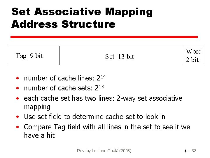
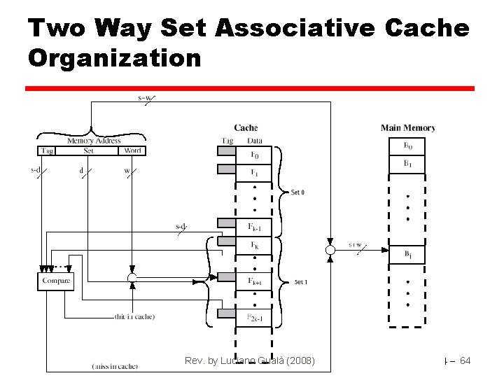
Set Associative Mapping Address Structure Tag 9 bit Set 13 bit Word 2 bit • number of cache lines: 214 • number of cache sets: 213 • each cache set has two lines: 2 -way set associative mapping • Use set field to determine cache set to look in • Compare Tag field with all lines in the set to see if we have a hit Rev. by Luciano Gualà (2008) 4 - 63

Two Way Set Associative Cache Organization Rev. by Luciano Gualà (2008) 4 - 64

Replacement Algorithms (1) Direct mapping • No choice • Each block only maps to one line • Replace that line Rev. by Luciano Gualà (2008) 4 - 65

Replacement Algorithms (2) Associative & Set Associative • Hardware implemented algorithm (to obtain speed) • Least Recently used (LRU) • e. g. in 2 way set associative § Which of the 2 blocks is LRU? • First in first out (FIFO) § replace block that has been in cache longest • Least frequently used § replace block which has had fewest hits • Random § Almost as good as LRU Rev. by Luciano Gualà (2008) 4 - 66

Write Policy • Multiple CPUs may have individual caches • I/O may address main memory directly cache(s) and main memory may become non-consistent Rev. by Luciano Gualà (2008) 4 - 67

Write through • All writes go to main memory as well as cache • Multiple CPUs can monitor main memory traffic to keep local (to CPU) cache up to date • Lots of traffic • Slows down writes Rev. by Luciano Gualà (2008) 4 - 68

Write back • Updates initially made in cache only • Update bit for cache slot is set when update occurs • If block has to be replaced, write to main memory only if update bit is set • I/O must access main memory through cache • N. B. 15% of memory references are writes • Caches of other devices get out of sync § Cache coherency problem (a general problem in distributed systems !) Rev. by Luciano Gualà (2008) 4 - 69

Block Size • Too small § Locality of reference is not used • Too large § Locality of reference is lost • Typical block size: 8 – 32 bytes Rev. by Luciano Gualà (2008) 4 - 70

Number of Caches • 2 levels of cache § L 1 on chip (since technology allows it) § L 2 on board (to fill the speed gap) • 2 kinds of cache § Data cache § Instruction cache § To allow instruction parallel processing and data fetching interfere Rev. by Luciano Gualà (2008) 4 - 71